
Design Review
For
DC-DC Converter for EWB Wind Turbine Project
ECE445 – Senior Design
Developers
Chris Livesay
Jeong-Ah Lee
Qing Janet Wang
Date
February 22, 2006

DC-DC Converter for EWB Wind Turbine Project
I. Introduction
This project is part of an ongoing project for Engineers Without Borders (EWB) and will be a
great opportunity to help the lives of underprivileged people while giving us practical hands-on
experience in the field of power engineering.
Objectives:
For this project, we will be designing a dc-dc converter that connects a wind turbine output
ranging from 40 to 70 volts to a charge controller used to charge 12 volt lead-acid batteries. The
dc-dc converter will be used to improve a village’s access to electricity from wind sources in
India.
Benefits:
- Provides a reliable and low cost way to improve access to electricity
- Achieves high efficiency (approximately 85%)
- Does not create radio frequency interference
- Does not drain battery when wind turbine is not producing power
Features:
- Output is user-adjustable between 12V - 8 A and 15V - 10 A, regulated
- Able to take full output of wind generator when load is switched on
- Input over-voltage protection
- Input and output overload protection
- Input and output short circuit protection
- Input and output reverse polarity protection
1

II. Design
Block Diagram:
Block Descriptions:
DC-DC Buck Converter
1.
The dc-dc converter will be capable of converting an input of 35 to 85 Volts dc to
an output of 12 to 15 Volts dc.
2.
The input protection and the MOSFET driver will be connected as inputs while
the output protection will be connected at the output.
Input Protection
1.
The input protection will protect against an input short-circuit, input reverse
polarity and input overload.
2.
The input voltage (wind turbine output) may exceed 125 V if a wire breaks and
the load is disconnected, so our circuit will provide protection up to 170 V.
3.
The wind turbine output will be connected here and the output of the input
protection will be connected to the dc-dc converter input.
4.
The main purpose is to keep the dc-dc converter from being damaged.
MOSFET Driver
1.
This component will be used to drive the converter MOSFETs.
2.
It will also protect against input over-voltage.
3.
It will be connected to the MOSFETs in the dc-dc converter.
Output Protection
1.
The output protection will protect against an output short-circuit, output reverse
polarity and output overload.
2.
The dc-dc converter output will be connected to this part and the load will be
connected to the output.
3.
The purpose of this part is to protect the dc-dc converter and also the load.
2

Performance Requirement:
With an input of around 35 V to 85 V, the output of the dc-dc converter should be regulated at 12
V and 8 A or 15 V and 10 A. The voltage ripple should be less than ±0.5% of the output. The
desired efficiency is around 85 %. The converter should be user-settable for an output of 12 to
15 Volts.
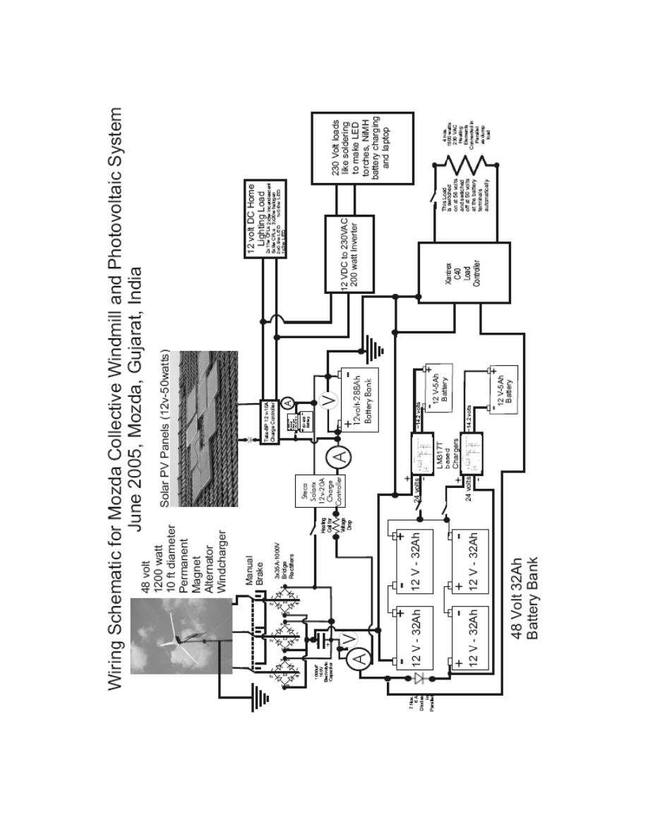
For reference, the wind generator details are given below:
1.
Its dc output, ranging from 40 V – 70 V, feeds into the dc-dc converter.
2.
Mozda HAWT is a 48 volt, 1200 VA, star connected three phase ac generator [12
pole rotor (the rotor is a set of two mild steel disks of 8" diameter each with 12
neodymium iron boron magnets of 2" x 1" x 1/2" size, Grade 35), 9 coil stator
(each coil made from 1.1 mm diameter enameled copper wire with 140 turns
wound so that the hollow of the coil has the size of the magnet)].
3.
The design of the generator is for 170 rpm cut-in and 600 or 700 rpm max output.
4.
Normally, the maximum voltage is around 65 V, but in case some wire breaks etc.
and the generator disconnects, then the voltage may exceed 125 V.
Schematics:
See next 4 pages for schematics and calculations.
3
4
Dc-dc Converter Schematic:
M
O
SFE
T
IRF
640
V
ra
te
d
=
200V
I
ra
te
d
=
18A
Fuse
h
o
ld
er
HTB-
24I
Fuse
S
iz
e
1
4
" x
1
1
4
"
V
ra
te
d
= 25
0
V
I
ra
te
d
=
1
5
A
V
IN
Di
o
d
e x
2
MBR10100
V
ra
te
d
=
100V
I
ra
te
d
=
10A
Di
ode
MR756 OR MR752
V
ra
te
d
(R
M
S
)
=
420V
I
ra
te
d
=
22A
In
du
ct
or
T
106-26
Core
L
10
m
H
N=
11
B=
.2T
E
lect
rolytic
C
ap
acitor
x
5
C
50
m
F
V
ra
te
d
=
150V
Fu
se
A
BC-15
V
ra
te
d
=
2
5
0V
I
ra
te
d
=
15A
V
OU
T
Fu
se
A
BC-6
V
ra
te
d
=
2
5
0V
I
ra
te
d
= 6A
Fuse
h
o
ld
er
HT
B-24I
Fuse
S
iz
e
1
4
" x
1
1
4
"
V
ra
te
d
= 250V
I
ra
te
d
=
1
5
A
GN
D
IN
Connec
t
to C
as
e
Con
n
ect
to C
as
e
GND
OU
T
Di
o
d
e
MR75
6
OR MR752
V
ra
te
d(R
M
S
)
=
420V
I
ra
te
d
=
22A
PWM
5
PWM Control Schematic
TL5
98
1-
1I
N+
2-
1
IN
-
3-
F
E
ED
BA
CK
4-
DT
C
8-OU
T
1
7-
SI
GNAL GND
6-
RT
5-C
T
Vcc-
1
2
Vc-11
PO
WE
R
GND-10
OUT
2-9
OUTP
U
T CTR
L
-13
RE
F
-14
2I
N--
1
5
2I
N+-
1
6
NC
-8
OU
T
A
-7
Vs-6
OUT
B
-5
4-
IN
B
3-GND
2-
INA
1-N
C
MIC44
2
7
TL
43
1
1-
CAT
H
2-
NC
3-
NC
4-
NC
NC-5
ANODE-6
NC-7
REF-
8
PWM
1k
W
50
W
V
IN
20
k
W+
2k
W
15
0k
W
V
OUT
20k
W
POT
50k
W
.0
1
m
F
47
0
W
+
30
W
1k
W
39
k
W
15
0k
W
V
IN
5V
Thi
s POT c
o
nt
ro
ls
the
o
u
tpu
t vo
lt
age ra
nge,
12
V-
15
V
33
0
W
V
IN
2
20k
W
5k
W
Whe
n
the vo
ltag
e
d
ivi
der re
aches
1.8
6
V (
V
IN
=
8
5
V
)
th
e TL431
will
c
o
nduct a
nd
the
TL598 w
il
l
turn off.
These deter
m
ine
the
fr
eq
uenc
y, f=1
/(
2
*
R
*
C
)
10
k
W
PN
P
B
JT
2N29
0
5
V
ra
te
d
= 4
0
V
I
ra
te
d
=
150
mA
6

Calculations:
Design Specifications
35
85
12
15
1.5
8
1
96
150
100
IN
OUT
OUT
OUT
OUT
SW
V
V
V
V
V
V
R
A
I
A
W
P
W
0
f
kHz
<
<
<
<
=
Ω
<
<
<
<
=
Duty Ratio Limits
12
15
85
35
.141
.429
OUT
IN
V
D
V
D
D
=
< <
< <
Input Current Limits
*
.141*8
.429 *10
1.128
4.290
IN
OUT
IN
IN
I
D I
I
A
I
A
=
<
<
<
<
Capacitor Design
*
*
.429
.01*1.5*100000
286
OUT
SW
D
C
I
V
f
C
C
F
µ
=
∆
=
>
Inductor Design
(
)
(
)
(
)
6
*
1
2
1
2 *
1.5
1 .141
2 *100000
6.443
10
*
*
10 *10 *.0649
75*
*.000066
11
OUT
CRIT
OUT
CRIT
CRIT
CRIT
o
R
T
L
D
R
L
D
f
L
L
F
L
F
L l
N
A
N
N
µ
µ
µ
µ
−
=
−
=
−
=
−
=
=
=
=
=
max
max
max
*
*
75*
*11*10
.0649
.160
OUT
o
N I
B
l
B
B
T
µ
µ
=
=
=
7
Simulation Results and Schematic:
The following graphs illustrate the preliminary simulation results for the buck converter. The
schematic of the buck converter is attached in the following page. We used a switch to simulate
the MOSFET. We set the period to 10 µs. We tested the converter at the input of 35 V, the
minimum voltage at which the PWM and the MOSFET driver turn on, and at 85 V, the
maximum voltage the shunt regulator can handle before shutting down. For an input of 35 V, we
achieved the desired output of 15 V by setting the duty ratio to 0.612. For an input of 85 V, the
desired output was achieved with the duty ratio of 0.205.
Time
0s
0.5ms
1.0ms
1.5ms
2.0ms
2.5ms
3.0ms
3.5ms
4.0ms
4.5ms
5.0ms
V(R1:2)
0V
4V
8V
12V
16V
Vout = 15 V
Vin = 35 V
Vin = 35 V; Vout = 15 V; D=0.612
Time
0s
0.5ms
1.0ms
1.5ms
2.0ms
2.5ms
3.0ms
3.5ms
4.0ms
4.5ms
5.0ms
V(R1:2)
0V
5V
10V
15V
20V
Vout = 15 V
Vin = 85 V
Vin = 85 V; Vout = 15 V; D=0.205
7

THE PSPICE SIMULATION SCHEMATIC WILL GO HERE.
8

III. Verification
Testing Procedures:
Besides testing how well all the components work together, we want to make sure that all parts
of our circuit are independently operating to our satisfaction. The testing of each component is
described in their respective locations below.
Dc-dc Converter
Our dc-dc converter will be tested in the lab. The output voltage will be plotted with respect to
the input voltage ranging from 0 V to 170 V. To obtain the needed dc input voltage several
power supplies will be connected in series. From this data the line regulation can be calculated.
Efficiency will be calculated and plotted by taking the output power divided by the input power
over the input voltage range of 35 V to 85 V. If the efficiency does not reach the minimum value
of 85%, we may have to modify our design.
Over-voltage Protection
Over-voltage protection will be tested by simply increasing the voltage above 85 V until about
150 V (the maximum voltage the wind turbine output can reach) and checking to make sure the
circuit turns off. Reverse polarity will be tested by reversing the polarity of the input and making
sure the fuse blows without harming any of the other components. Overload protection will be
tested by overloading the circuit to above 15 A (the rated current of the fuse holder) and again,
making sure the fuse blows. Overload will be achieved by placing a small high power resistor at
the output.
MOSFET Driver
We will take a look at the PWM signal coming out of the MIC4427. We will identify the square
wave pulse occurring accordingly to the required duty ratio which ranges from 0.141 to 0.429.
We will also note the amplitude of the signal.
Tolerance Analysis:
The one component that will affect the output of the dc-dc converter the most is the output
voltage capacitor filter. The size of the capacitor will determine the amount of voltage ripple that
will be present at the output. Since the project proposal from EWB does not provide a specific
ripple allowance, we will set the ripple allowance specification to ±0.5% of the output voltage.
To achieve this, we will be testing the filter circuit under various sized capacitors to find the
smallest capacitor value we can have and still maintain a ripple voltage under the allowed
amount.
9

IV.
Cost and Schedule
Cost Analysis:
• Parts
Parts Received
Part #
Mft
Desc Price
Qty Total
MIC4427YN
Micrel Inc
MOSFET Driver 1.5A
$1.95
1
$1.95
TL431CP
Texas
Instruments
Shunt Regulator
$0.40 1 $0.40
TL598CN
Texas
Instruments
PWM Controller
$1.35 1 $1.35
Total
$3.70
Parts Needed
Part #
Mft
Desc Price
Qty
Total
HTB-24I
Ferraz
Shawmut
Fuseholder ¼” x 1 ¼”
250V 15A
$2.80 2 $5.60
IRF640
International
Rectifier
MOSFET
200V 18A
$1.99 1 $1.99
MR756 or
MR752
ON
Semiconductor
Diode 50-1000 V
$0.70 2 $1.40
2N2905 SECOA
PNP
BJT
$0.45
1
$0.45
T106-26
Micrometals
Powdered Metal Core
$1.50
1
$1.50
N/A
Parts Shop
PCB Board
$30.00 1
$30.00
N/A
Parts Shop
Containment Box
$3.50
1
$3.50
N/A ERJ
Various
RES
$0.04
15
$0.60
N/A Lab
Various
CAP
$1.50
5
$7.50
N/A Lab
12
Gauge
Wire
$3.00
1
$3.00
Total
$59.24
• Labor
$40/hour x 2.5 x 70 hours x 3 people = $21,000
• Grand Total
Parts + Labor = ($3.70 +$59.24) + $21,000 = $21,062.94
10

Schedule:
Week Of
Description
01/30/06 Brainstorm
Design
Alternative – Everyone
Proposal – Janet
02/06/06
Finish Proposal – Jeong
Finalize Design -- Chris
Draw Circuit Schematics – Chris
Order Parts -- Janet
* Proposal due 2/8 @ 4PM
02/13/06
Create Simulations of Converter – Jeong
Create Simulations of MOSFET – Jeong
Write Design Report – Chris
Receive Parts -- Janet
* Design Review sign-up opens 2/13
02/20/06
Build Converter -- Chris
Build Output Filter -- Jeong
Build Control Circuit -- Janet
* Design Review 2/22-2/24
02/27/06
Modular Testing – Chris
03/06/06
Debug – Jeong
Integrate Prototype – Janet
03/13/06
Final Optimization/Testing -- Chris
Order PCB Board -- Jeong
Prepare Mock-Up – Janet
03/20/06 Spring
Break
03/27/06
Mock Demo – Everyone
04/03/06
Prepare Presentation – Jeong
Receive PCB Board -- Jeong
Final Optimization – Chris
04/10/06
Final Paper – Janet
* Demos & Presentation sign-up opens 4/14
04/17/06
Final Presentation – Everyone
04/24/06
Demo & Presentation – Everyone
05/01/06
Relax – Everyone
* Final Papers & Lab Notebooks due 5/2 @ 4 PM
* Check Out & Awards 5/4 @ 4-6PM
11
Wyszukiwarka
Podobne podstrony:
Boost Converter Design For 20Kw Wind Turbine Generator
Development Of A Single Phase Inverter For Small Wind Turbine
The Material Selection for Typical Wind Turbine Blades 2006
Development Of High Frequency Link Direct Dc To Ac Converters For Link Direct Dc To Ac Converters Fo
Blade sections for wind turbine and tidal current turbine applications—current status and future cha
Innovative Solutions In Power Electronics For Variable Speed Wind Turbines
Modeling Of The Wind Turbine With A Doubly Fed Induction Generator For Grid Integration Studies
Development of wind turbine control algorithms for industrial use
Compliant Blades For Wind Turbines
DC DC Converters k99e25 l1120
Advanced Methods for Development of Wind turbine models for control designe
ANALYSIS OF CONTROL STRATEGIES OF A FULL CONVERTER IN A DIRECT DRIVE WIND TURBINE
Synchronous Generator And Frequency Converter In Wind Turbine Applications System Design And Efficie
0 Alternative Composite Materials for Megawatt Scale Wind Turbines Griffin Ashwill 2003
A Low Speed, High Torque, Direct Drive Permanent Magnet Generator For Wind Turbines
IFL90 ch4 DC DC Converter intel
więcej podobnych podstron