3-Axis, ±2 g/±4 g/±8 g/±16 g
Digital Accelerometer
Rev. C
Information furnished by Analog Devices is believed to be accurate and reliable. However, no
responsibility is assumed by Analog Devices for its use, nor for any infringements of patents or other
rights of third parties that may result from its use. Specifications subject to change without notice. No
license is granted by implication or otherwise under any patent or patent rights of Analog Devices.
Trademarks and registered trademarks are the property of their respective owners. See the last
page for disclaimers.
One Technology Way, P.O. Box 9106, Norwood, MA 02062-9106, U.S.A.
Tel: 781.329.4700
www.analog.com
Fax: 781.461.3113
©2009–2011 Analog Devices, Inc. All rights reserved.
FEATURES
Ultralow power: as low as 23 μA in measurement mode and
0.1 μA in standby mode at V
S
= 2.5 V (typical)
Power consumption scales automatically with bandwidth
User-selectable resolution
Fixed 10-bit resolution
Full resolution, where resolution increases with g range,
up to 13-bit resolution at ±16 g (maintaining 4 mg/LSB
scale factor in all g ranges)
Patent pending, embedded memory management system
with FIFO technology minimizes host processor load
Single tap/double tap detection
Activity/inactivity monitoring
Free-fall detection
Supply voltage range: 2.0 V to 3.6 V
I/O voltage range: 1.7 V to V
S
SPI (3- and 4-wire) and I
2
C digital interfaces
Flexible interrupt modes mappable to either interrupt pin
Measurement ranges selectable via serial command
Bandwidth selectable via serial command
Wide temperature range (−40°C to +85°C)
10,000 g shock survival
Pb free/RoHS compliant
Small and thin: 3 mm × 5 mm × 1 mm LGA package
APPLICATIONS
Handsets
Medical instrumentation
Gaming and pointing devices
Industrial instrumentation
Personal navigation devices
Hard disk drive (HDD) protection
GENERAL DESCRIPTION
The ADXL345 is a small, thin, ultralow power, 3-axis accelerometer
with high resolution (13-bit) measurement at up to ±16 g. Digital
output data is formatted as 16-bit twos complement and is acces-
sible through either a SPI (3- or 4-wire) or I
2
C digital interface.
The ADXL345 is well suited for mobile device applications. It
measures the static acceleration of gravity in tilt-sensing appli-
cations, as well as dynamic acceleration resulting from motion
or shock. Its high resolution (3.9 mg/LSB) enables measurement
of inclination changes less than 1.0°.
Several special sensing functions are provided. Activity and
inactivity sensing detect the presence or lack of motion by
comparing the acceleration on any axis with user-set thresholds.
Tap sensing detects single and double taps in any direction. Free-
fall sensing detects if the device is falling. These functions can
be mapped individually to either of two interrupt output pins.
An integrated, patent pending memory management system with a
32-level first in, first out (FIFO) buffer can be used to store data to
minimize host processor activity and lower overall system power
consumption.
Low power modes enable intelligent motion-based power
management with threshold sensing and active acceleration
measurement at extremely low power dissipation.
The ADXL345 is supplied in a small, thin, 3 mm × 5 mm × 1 mm,
14-lead, plastic package.
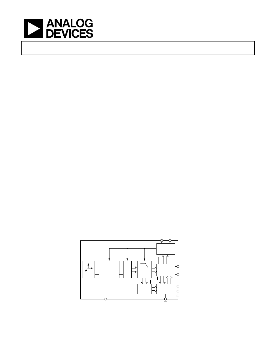
FUNCTIONAL BLOCK DIAGRAM
3-AXIS
SENSOR
SENSE
ELECTRONICS
DIGITAL
FILTER
ADXL345
POWER
MANAGEMENT
CONTROL
AND
INTERRUPT
LOGIC
SERIAL I/O
INT1
V
S
V
DD I/O
INT2
SDA/SDI/SDIO
SDO/ALT
ADDRESS
SCL/SCLK
GND
ADC
32 LEVEL
FIFO
CS
07925-
001
Figure 1.

ADXL345
Rev. C | Page 2 of 40
TABLE OF CONTENTS
General Description ......................................................................... 1
Functional Block Diagram .............................................................. 1
Revision History ............................................................................... 3
Absolute Maximum Ratings............................................................ 6
Thermal Resistance ...................................................................... 6
Package Information .................................................................... 6
ESD Caution.................................................................................. 6
Pin Configuration and Function Descriptions............................. 7
Typical Performance Characteristics ............................................. 8
Theory of Operation ...................................................................... 13
Power Sequencing ...................................................................... 13
Power Savings ............................................................................. 14
Serial Communications ................................................................. 15
Interrupts..................................................................................... 20
Self-Test ....................................................................................... 22
Register Map ................................................................................... 23
Register Definitions ................................................................... 24
Applications Information .............................................................. 28
Power Supply Decoupling ......................................................... 28
Mechanical Considerations for Mounting.............................. 28
Tap Detection.............................................................................. 28
Threshold .................................................................................... 29
Link Mode ................................................................................... 29
Sleep Mode vs. Low Power Mode............................................. 30
Offset Calibration....................................................................... 30
Using Self-Test ............................................................................ 31
Data Formatting of Upper Data Rates..................................... 32
Noise Performance ..................................................................... 33
Operation at Voltages Other Than 2.5 V ................................ 33
Offset Performance at Lowest Data Rates............................... 34
Axes of Acceleration Sensitivity ............................................... 35
Layout and Design Recommendations ................................... 36
Outline Dimensions ....................................................................... 37
Ordering Guide .......................................................................... 37

ADXL345
Rev. C | Page 3 of 40
REVISION HISTORY
5/11—Rev. B to Rev. C
Added Preventing Bus Traffic Errors Section ............................15
Changes to Figure 37, Figure 38, Figure 39 .................................16
Changes to Table 12 ........................................................................19
Changes to Using Self-Test Section...............................................31
Changes to Axes of Acceleration Sensitivity Section..................35
11/10—Rev. A to Rev. B
Change to 0 g Offset vs. Temperature for Z-Axis Parameter,
Table 1 .................................................................................................4
Changes to Figure 10 to Figure 15 ..................................................9
Changes to Ordering Guide...........................................................37
4/10—Rev. 0 to Rev. A
Changes to Features Section and General
Description Section...........................................................................1
Changes to Specifications Section...................................................3
Changes to Table 2 and Table 3 .......................................................5
Added Package Information Section, Figure 2, and Table 4;
Renumbered Sequentially ................................................................5
Changes to Pin 12 Description, Table 5 .........................................6
Added Typical Performance Characteristics Section ...................7
Changes to Theory of Operation Section and Power Sequencing
Section ..............................................................................................12
Changes to Powers Savings Section, Table 7, Table 8, Auto Sleep
Mode Section, and Standby Mode Section ..................................13
Changes to SPI Section...................................................................14
Changes to Figure 36 to Figure 38 ................................................15
Changes to Table 9 and Table 10 ...................................................16
Changes to I
2
C Section and Table 11 ............................................17
Changes to Table 12 ........................................................................18
Changes to Interrupts Section, Activity Section, Inactivity
Section, and FREE_FALL Section.................................................19
Added Table 13 ................................................................................19
Changes to FIFO Section ...............................................................20
Changes to Self-Test Section and Table 15 to Table 18 ..............21
Added Figures 42 and Table 14 .....................................................21
Changes to Table 19 ........................................................................22
Changes to Register 0x1D—THRESH_TAP (Read/Write)
Section, Register 0x1E, Register 0x1F, Register 0x20—OFSX,
OFSY, OSXZ (Read/Write) Section, Register 0x21—DUR
(Read/Write) Section, Register 0x22—Latent (Read/Write)
Section, and Register 0x23—Window (Read/Write) Section ...23
Changes to ACT_X Enable Bits and INACT_X Enable Bit
Section, Register 0x28—THRESH_FF (Read/Write) Section,
Register 0x29—TIME_FF (Read/Write) Section, Asleep Bit
Section, and AUTO_SLEEP Bit Section.......................................24
Changes to Sleep Bit Section .........................................................25
Changes to Power Supply Decoupling Section, Mechanical
Considerations for Mounting Section, and Tap Detection
Section ..............................................................................................27
Changes to Threshold Section.......................................................28
Changes to Sleep Mode vs. Low Power Mode Section...............29
Added Offset Calibration Section.................................................29
Changes to Using Self-Test Section ..............................................30
Added Data Formatting of Upper Data Rates Section, Figure 48,
and Figure 49 ...................................................................................31
Added Noise Performance Section, Figure 50 to Figure 52, and
Operation at Voltages Other Than 2.5 V Section .......................32
Added Offset Performance at Lowest Data Rates Section and
Figure 53 to Figure 55.....................................................................33
6/09—Revision 0: Initial Version

ADXL345
Rev. C | Page 4 of 40
SPECIFICATIONS
T
A
= 25°C, V
S
= 2.5 V, V
DD I/O
= 1.8 V, acceleration = 0 g, C
S
= 10 μF tantalum, C
I/O
= 0.1 μF, output data rate (ODR) = 800 Hz, unless
otherwise noted. All minimum and maximum specifications are guaranteed. Typical specifications are not guaranteed.
Table 1.
Parameter Test
Conditions
Min
Typ
Unit
SENSOR INPUT
Each axis
Measurement Range
User selectable
±2, ±4, ±8, ±16
g
Nonlinearity
Percentage of full scale
±0.5
%
Inter-Axis Alignment Error
±0.1
Degrees
Cross-Axis Sensitivity
±1
%
OUTPUT RESOLUTION
Each axis
All g Ranges
10-bit resolution
10
Bits
±2 g Range
Full resolution
10
Bits
±4 g Range
Full resolution
11
Bits
±8 g Range
Full resolution
12
Bits
±16 g Range
Full resolution
13
Bits
SENSITIVITY
Each axis
Sensitivity at X
OUT
, Y
OUT
, Z
OUT
All
g-ranges, full resolution
230
256
282
LSB/g
±2
g, 10-bit resolution
230
256
282
LSB/g
±4
g, 10-bit resolution
115
128
141
LSB/g
±8
g, 10-bit
resolution
57 64
71 LSB/g
±16
g, 10-bit
resolution
29 32
35 LSB/g
Sensitivity Deviation from Ideal
All g-ranges
±1.0
%
Scale Factor at X
OUT
, Y
OUT
, Z
OUT
All g-ranges, full resolution
3.5
3.9
4.3
mg/LSB
±2
g, 10-bit resolution
3.5
3.9
4.3
mg/LSB
±4
g, 10-bit
resolution
7.1 7.8
8.7 mg/LSB
±8
g, 10-bit
resolution
14.1 15.6
17.5 mg/LSB
±16
g, 10-bit
resolution
28.6 31.2
34.5 mg/LSB
Sensitivity Change Due to Temperature
±0.01
%/°C
0 g OFFSET
Each axis
0 g Output for X
OUT
, Y
OUT
−150 0
+150 mg
0 g Output for Z
OUT
−250 0
+250 mg
0 g Output Deviation from Ideal, X
OUT
, Y
OUT
±35
mg
0 g Output Deviation from Ideal, Z
OUT
±40
mg
0 g Offset vs. Temperature for X-, Y-Axes
±0.4
mg/°C
0 g Offset vs. Temperature for Z-Axis
±1.2
mg/°C
NOISE
X-, Y-Axes
ODR = 100 Hz for ±2 g, 10-bit resolution or
all g-ranges, full resolution
0.75
LSB
rms
Z-Axis
ODR = 100 Hz for ±2 g, 10-bit resolution or
all g-ranges, full resolution
1.1
LSB
rms
OUTPUT DATA RATE AND BANDWIDTH
User selectable
Output Data Rate (ODR)
0.1
3200
Hz
SELF-TEST
Output Change in X-Axis
0.20
2.10
g
Output Change in Y-Axis
−2.10
−0.20
g
Output Change in Z-Axis
0.30
3.40
g
POWER
SUPPLY
Operating Voltage Range (V
S
)
2.0 2.5
3.6 V
Interface Voltage Range (V
DD I/O
)
1.7
1.8 V
S
V
Supply Current
ODR ≥ 100 Hz
140
μA
ODR < 10 Hz
30
μA
Standby Mode Leakage Current
0.1
μA
Turn-On and Wake-Up Time
ODR = 3200 Hz
1.4
ms

ADXL345
Rev. C | Page 5 of 40
Parameter Test
Conditions
Min
Typ
Max
Unit
TEMPERATURE
Operating
Temperature
Range
−40
+85 °C
WEIGHT
Device
Weight
30
mg
1
The typical specifications shown are for at least 68% of the population of parts and are based on the worst case of mean ±1 σ, except for 0 g output and sensitivity,
which represents the target value. For 0 g offset and sensitivity, the deviation from the ideal describes the worst case of mean ±1 σ.
2
Cross-axis sensitivity is defined as coupling between any two axes.
3
Bandwidth is the −3 dB frequency and is half the output data rate, bandwidth = ODR/2.
4
The output format for the 3200 Hz and 1600 Hz ODRs is different than the output format for the remaining ODRs. This difference is described in the Data Formatting of
5
Output data rates below 6.25 Hz exhibit additional offset shift with increased temperature, depending on selected output data rate. Refer to the Offset Performance at
Lowest Data Rates section for details.
6
Self-test change is defined as the output (g) when the SELF_TEST bit = 1 (in the DATA_FORMAT register, Address 0x31) minus the output (g) when the SELF_TEST bit =
0. Due to device filtering, the output reaches its final value after 4 × τ when enabling or disabling self-test, where τ = 1/(data rate). The part must be in normal power
operation (LOW_POWER bit = 0 in the BW_RATE register, Address 0x2C) for self-test to operate correctly.
7
Turn-on and wake-up times are determined by the user-defined bandwidth. At a 100 Hz data rate, the turn-on and wake-up times are each approximately 11.1 ms. For
other data rates, the turn-on and wake-up times are each approximately τ + 1.1 in milliseconds, where τ = 1/(data rate).
ADXL345
Rev. C | Page 6 of 40
ABSOLUTE MAXIMUM RATINGS
Table 2.
Parameter Rating
Acceleration
Any Axis, Unpowered
10,000 g
Any Axis, Powered
10,000 g
V
S
−0.3 V to +3.9 V
V
DD I/O
−0.3 V to +3.9 V
Digital Pins
−0.3 V to V
DD I/O
+ 0.3 V or 3.9 V,
whichever is less
All Other Pins
−0.3 V to +3.9 V
Output Short-Circuit Duration
(Any Pin to Ground)
Indefinite
Temperature Range
Powered
−40°C to +105°C
Storage
−40°C to +105°C
Stresses above those listed under Absolute Maximum Ratings
may cause permanent damage to the device. This is a stress
rating only; functional operation of the device at these or any
other conditions above those indicated in the operational
section of this specification is not implied. Exposure to absolute
maximum rating conditions for extended periods may affect
device reliability.
THERMAL RESISTANCE
Table 3. Package Characteristics
Package Type
θ
JA
θ
JC
Device
Weight
14-Terminal LGA
150°C/W
85°C/W
30 mg
PACKAGE INFORMATION
The information in Figure 2 and Table 4 provide details about
the package branding for the ADXL345. For a complete listing
of product availability, see the Ordering Guide section.
0
79
25
-10
2
3 4 5 B
# y w w
v v v v
C N T Y
Figure 2. Product Information on Package (Top View)
Table 4. Package Branding Information
Branding Key
Field Description
345B
Part identifier for ADXL345
# RoHS-compliant
designation
yww Date
code
vvvv
Factory lot code
CNTY
Country of origin
ESD CAUTION
ADXL345
Rev. C | Page 7 of 40
PIN CONFIGURATION AND FUNCTION DESCRIPTIONS
07
92
5-
0
02
CS
SDA/SDI/SDIO
SDO/ALT ADDRESS
RESERVED
NC
INT2
INT1
V
DD I/O
GND
RESERVED
GND
GND
V
S
13
12
11
10
9
8
1
2
3
4
+x
+y
+z
5
6
14
7
SCL/SCLK
ADXL345
TOP VIEW
(Not to Scale)
Figure 3. Pin Configuration (Top View)
Table 5. Pin Function Descriptions
Pin No.
Mnemonic
Description
1
V
DD I/O
Digital Interface Supply Voltage.
2
GND
This pin must be connected to ground.
3
RESERVED
Reserved. This pin must be connected to V
S
or left open.
4
GND
This pin must be connected to ground.
5
GND
This pin must be connected to ground.
6
V
S
Supply
Voltage.
7
CS
Chip Select.
8
INT1
Interrupt 1 Output.
9
INT2
Interrupt 2 Output.
10
NC
Not Internally Connected.
11
RESERVED
Reserved. This pin must be connected to ground or left open.
12
SDO/ALT ADDRESS
Serial Data Output (SPI 4-Wire)/Alternate I
2
C Address Select (I
2
C).
13
SDA/SDI/SDIO
Serial Data (I
2
C)/Serial Data Input (SPI 4-Wire)/Serial Data Input and Output (SPI 3-Wire).
14
SCL/SCLK
Serial Communications Clock. SCL is the clock for I
2
C, and SCLK is the clock for SPI.
ADXL345
Rev. C | Page 8 of 40
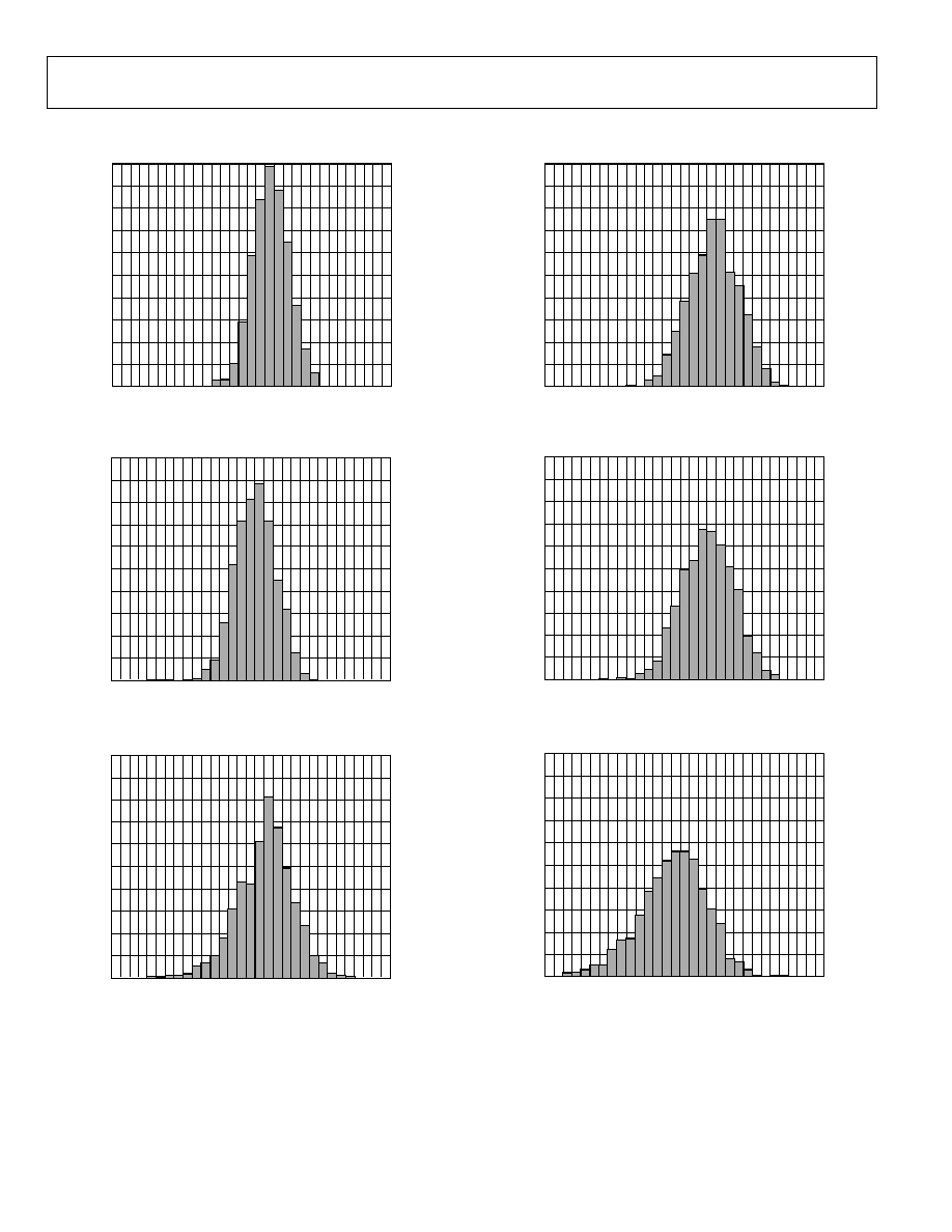
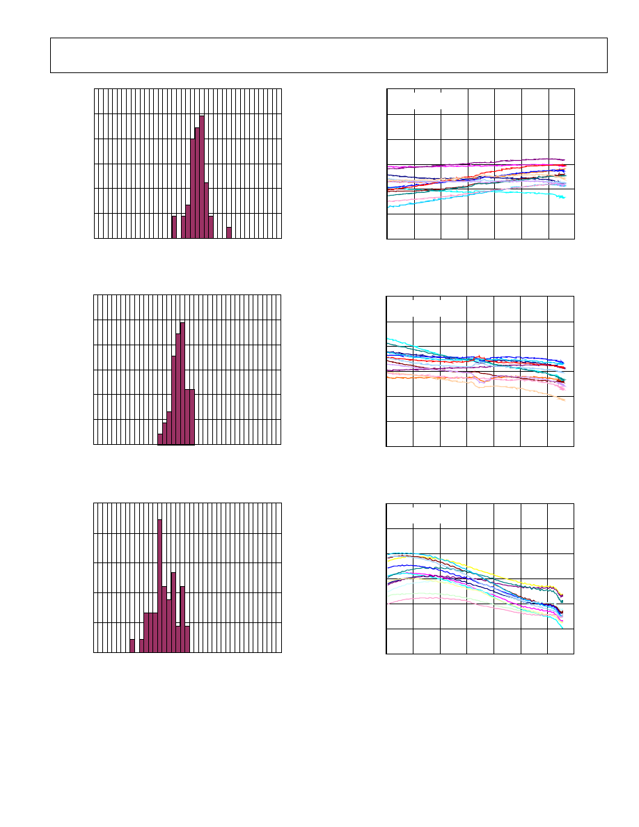
TYPICAL PERFORMANCE CHARACTERISTICS
0
2
4
6
8
10
12
14
16
18
20
–150
–100
–50
0
50
100
150
ZERO g OFFSET (mg)
P
ER
C
E
N
T
O
F
PO
PU
L
A
TI
O
N
(
%
)
07
92
5-
20
4
2
0
4
6
8
10
12
14
16
18
20
–150
–100
–50
0
50
100
150
ZERO g OFFSET (mg)
P
ER
C
E
N
T
O
F
PO
PU
L
A
TI
O
N
(
%
)
07
92
5-
20
7
Figure 4. X-Axis Zero g Offset at 25°C, V
S
= 2.5 V
Figure 7. X-Axis Zero g Offset at 25°C, V
S
= 3.3 V
2
0
4
6
8
10
12
14
16
18
20
–150
–100
–50
0
50
100
150
ZERO g OFFSET (mg)
PER
C
EN
T
O
F
PO
P
U
L
A
TI
O
N
(
%
)
07
92
5-
2
08
2
0
4
6
8
10
12
14
16
18
20
–150
–100
–50
0
50
100
150
ZERO g OFFSET (mg)
PE
R
C
EN
T
O
F
P
O
P
U
L
A
TI
O
N
(
%
)
07
92
5-
20
5
Figure 8. Y-Axis Zero g Offset at 25°C, V
S
= 3.3 V
Figure 5. Y-Axis Zero g Offset at 25°C, V
S
= 2.5 V
2
0
4
6
8
10
12
14
16
18
20
–150
–100
–50
0
50
100
150
ZERO g OFFSET (mg)
P
ER
C
E
N
T
O
F
PO
PU
L
A
TI
O
N
(
%
)
07
92
5-
20
9
2
0
4
6
8
10
12
14
16
18
20
–150
–100
–50
0
50
100
150
ZERO g OFFSET (mg)
P
ER
C
E
N
T
O
F
PO
PU
L
A
TI
O
N
(
%
)
07
92
5-
20
6
Figure 6. Z-Axis Zero g Offset at 25°C, V
S
= 2.5 V
Figure 9. Z-Axis Zero g Offset at 25°C, V
S
= 3.3 V
ADXL345
Rev. C | Page 9 of 40
0
5
10
15
20
25
30
–2.0
–1.5
–1.0
–0.5
0
0.5
1.0
1.5
2.0
ZERO g OFFSET TEMPERATURE COEFFICIENT (mg/°C)
P
E
RCE
NT
O
F
P
O
P
UL
A
TI
O
N
(
%
)
07
92
5-
2
10
Figure 10. X-Axis Zero g Offset Temperature Coefficient, V
S
= 2.5 V
–2.0
–1.5
–1.0
–0.5
0
0.5
1.0
1.5
2.0
ZERO g OFFSET TEMPERATURE COEFFICIENT (mg/°C)
P
E
RCE
NT
O
F
P
O
P
UL
A
TI
O
N
(
%
)
0
5
20
15
10
25
30
07
92
5-
2
11
Figure 11. Y-Axis Zero g Offset Temperature Coefficient, V
S
= 2.5 V
–2.0
–1.5
–1.0
–0.5
0
0.5
1.0
1.5
2.0
ZERO g OFFSET TEMPERATURE COEFFICIENT (mg/°C)
P
E
RCE
NT
O
F
P
O
P
UL
A
TI
O
N
(
%
)
0
5
20
15
10
25
07
92
5-
2
12
Figure 12. Z-Axis Zero g Offset Temperature Coefficient, V
S
= 2.5 V
–150
–100
–50
0
50
100
150
–40
–20
0
20
40
60
80
100
TEMPERATURE (°C)
OU
TP
U
T
(
m
g
)
N = 16
AVDD = DVDD = 2.5V
07
92
5-
2
13
Figure 13. X-Axis Zero g Offset vs. Temperature—
Eight Parts Soldered to PCB, V
S
= 2.5 V
–150
–100
–50
0
50
100
150
–40
–20
0
20
40
60
80
100
TEMPERATURE (°C)
OU
TP
U
T
(
m
g
)
N = 16
AVDD = DVDD = 2.5V
07
92
5-
2
14
Figure 14. Y-Axis Zero g Offset vs. Temperature—
Eight Parts Soldered to PCB, V
S
= 2.5 V
–150
–100
–50
0
50
100
150
–40
–20
0
20
40
60
80
100
TEMPERATURE (°C)
OU
TP
U
T
(
m
g
)
N = 16
AVDD = DVDD = 2.5V
07
92
5-
2
15
Figure 15. Z-Axis Zero g Offset vs. Temperature—
Eight Parts Soldered to PCB, V
S
= 2.5 V
ADXL345
Rev. C | Page 10 of 40
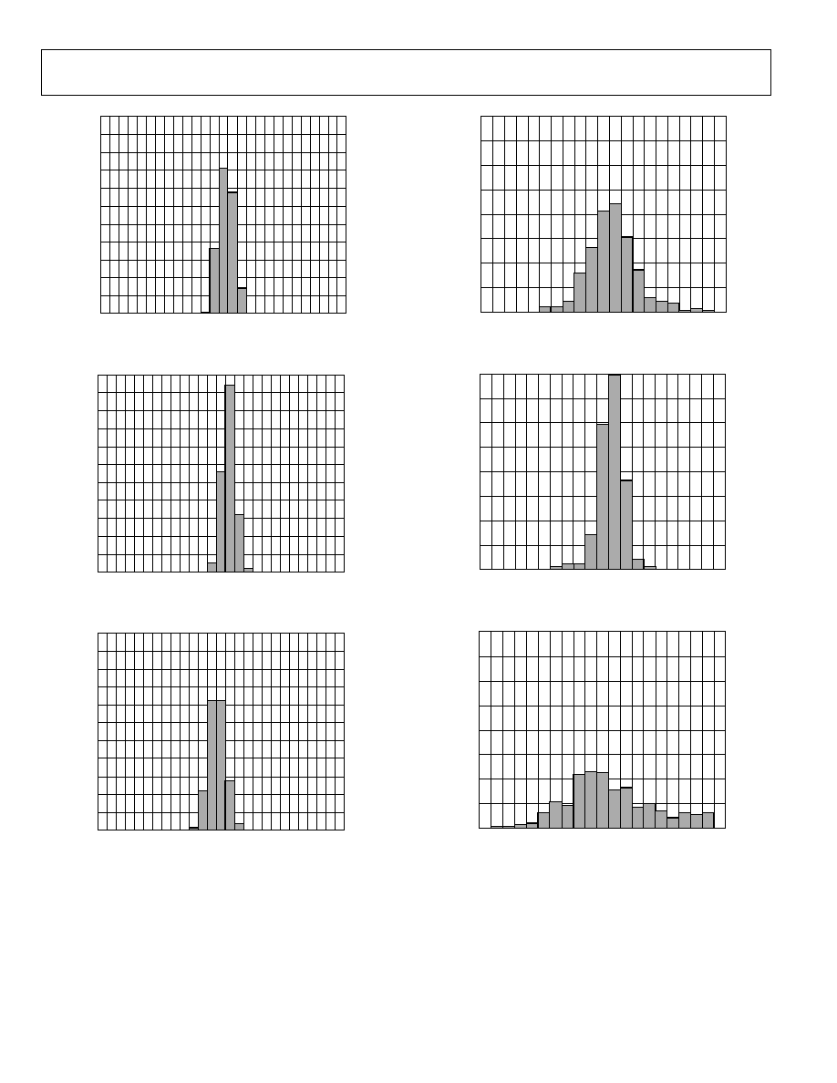
0
5
10
15
20
25
30
35
40
45
50
55
230 234 238 242 246 250 254 258 262 266 270 274 278 282
SENSITIVITY (LSB/g)
PER
C
EN
T
O
F
PO
P
U
L
A
TI
O
N
(
%
)
07
92
5-
21
6
Figure 16. X-Axis Sensitivity at 25°C, V
S
= 2.5 V, Full Resolution
0
5
10
15
20
25
30
35
40
45
50
55
230 234 238 242 246 250 254 258 262 266 270 274 278 282
SENSITIVITY (LSB/g)
PER
C
EN
T
O
F
PO
P
U
L
A
TI
O
N
(
%
)
07
92
5-
21
7
Figure 17. Y-Axis Sensitivity at 25°C, V
S
= 2.5 V, Full Resolution
0
5
10
15
20
25
30
35
40
45
50
55
230 234 238 242 246 250 254 258 262 266 270 274 278 282
SENSITIVITY (LSB/g)
P
E
RCE
NT
O
F
P
O
P
U
L
A
TI
O
N
(
%
)
07
92
5-
21
8
Figure 18. Z-Axis Sensitivity at 25°C, V
S
= 2.5 V, Full Resolution
0
5
10
15
20
25
30
35
40
–0.02
–0.01
0
0.01
0.02
SENSITIVITY TEMPERATURE COEFFICIENT (%/°C)
P
E
RCE
NT
O
F
P
O
P
UL
A
TI
O
N
(
%
)
07
92
5-
21
9
Figure 19. X-Axis Sensitivity Temperature Coefficient, V
S
= 2.5 V
0
5
10
15
20
25
30
35
40
–0.02
–0.01
0
0.01
0.02
SENSITIVITY TEMPERATURE COEFFICIENT (%/°C)
P
E
RCE
NT
O
F
P
O
P
UL
A
TIO
N
(
%
)
07
92
5-
2
20
Figure 20. Y-Axis Sensitivity Temperature Coefficient, V
S
= 2.5 V
0
5
10
15
20
25
30
35
40
–0.02
–0.01
0
0.01
0.02
SENSITIVITY TEMPERATURE COEFFICIENT (%/°C)
PE
R
C
EN
T
O
F
PO
PU
L
A
TI
O
N
(
%
)
0
7
925
-22
1
Figure 21. Z-Axis Sensitivity Temperature Coefficient, V
S
= 2.5 V
ADXL345
Rev. C | Page 11 of 40
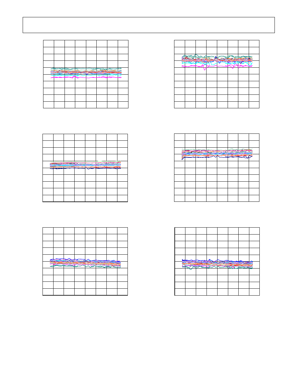
0
20
40
60
80
100
120
TEMPERATURE (°C)
230
235
240
245
250
255
260
265
270
275
280
S
E
N
S
IT
IV
IT
Y
(
L
S
B
/g
)
–40
–20
0
79
25
-22
2
Figure 22. X-Axis Sensitivity vs. Temperature—
Eight Parts Soldered to PCB, V
S
= 2.5 V, Full Resolution
230
235
240
245
250
255
260
265
270
275
280
TEMPERATURE (°C)
SEN
SI
T
IV
IT
Y
(
L
SB
/g
)
0
20
40
60
80
100
120
–40
–20
07
92
5-
2
23
Figure 23. Y-Axis Sensitivity vs. Temperature—
Eight Parts Soldered to PCB, V
S
= 2.5 V, Full Resolution
230
235
240
245
250
255
260
265
270
275
280
TEMPERATURE (°C)
SEN
SI
T
IV
IT
Y
(
L
SB
/g
)
0
20
40
60
80
100
120
–40
–20
07
92
5-
2
24
Figure 24. Z-Axis Sensitivity vs. Temperature—
Eight Parts Soldered to PCB, V
S
= 2.5 V, Full Resolution
TEMPERATURE (°C)
230
235
240
245
250
255
260
265
270
275
280
SEN
SI
T
IV
IT
Y
(
L
SB
/g
)
0
20
40
60
80
100
120
–40
–20
07
92
5-
2
25
Figure 25. X-Axis Sensitivity vs. Temperature—
Eight Parts Soldered to PCB, V
S
= 3.3 V, Full Resolution
0
20
40
60
80
100
120
TEMPERATURE (°C)
230
235
240
245
250
255
260
265
270
275
280
S
E
N
S
IT
IV
IT
Y
(
L
S
B
/g
)
–40
–20
07
92
5-
2
26
Figure 26. Y-Axis Sensitivity vs. Temperature—
Eight Parts Soldered to PCB, V
S
= 3.3 V, Full Resolution
0
20
40
60
80
100
120
TEMPERATURE (°C)
230
235
240
245
250
255
260
265
270
275
280
S
E
N
S
IT
IV
IT
Y
(
L
S
B
/g
)
–40
–20
07
92
5-
22
7
Figure 27. Z-Axis Sensitivity vs. Temperature—
Eight Parts Soldered to PCB, V
S
= 3.3 V, Full Resolution
ADXL345
Rev. C | Page 12 of 40
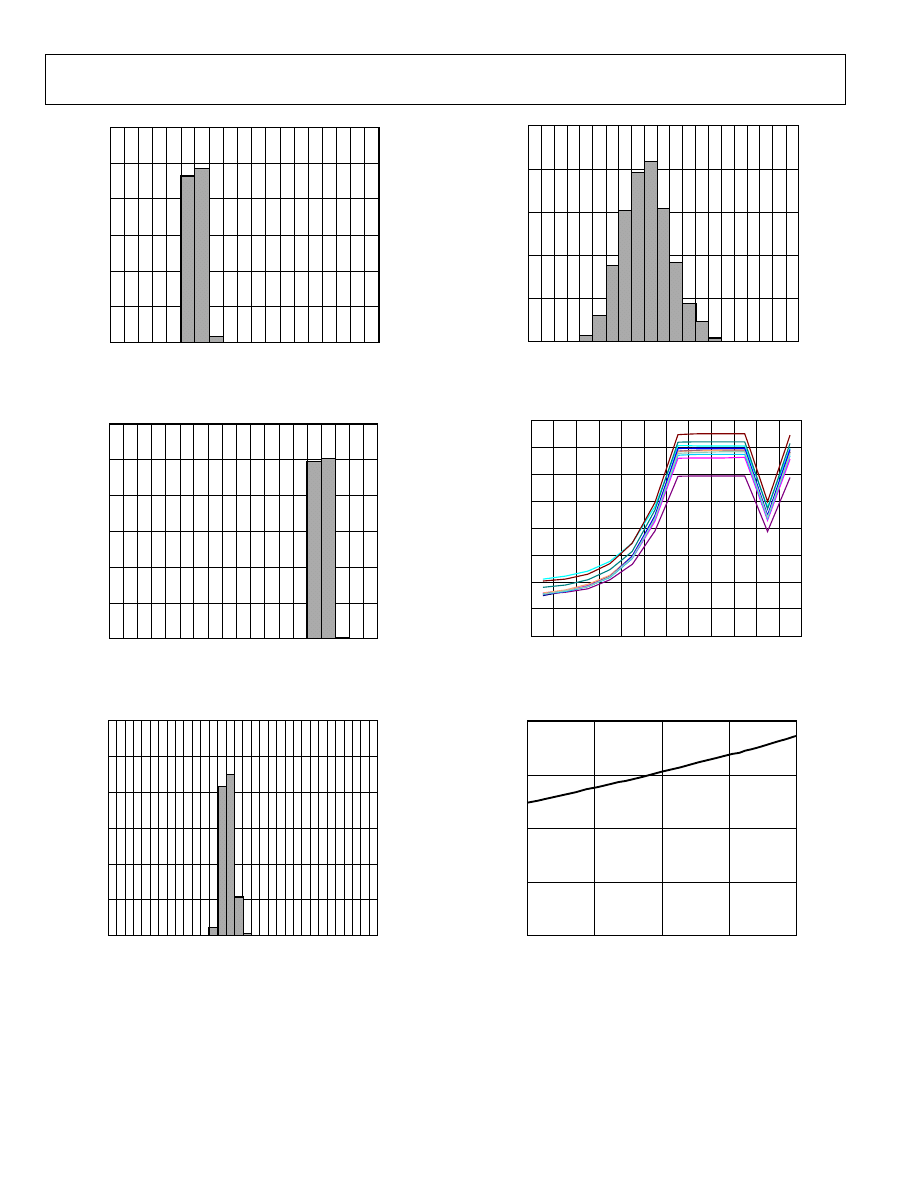
0
10
20
30
40
50
60
0.2
0.5
0.8
1.1
1.4
1.7
2.0
SELF-TEST RESPONSE (g)
P
E
RCE
NT
O
F
P
O
P
UL
A
TI
O
N
(
%
)
07
92
5-
2
28
0
5
10
15
20
25
100
110
120
130
140
150
160
170
180
190
200
CURRENT CONSUMPTION (µA)
P
ER
C
E
N
T
O
F
PO
PU
L
A
TIO
N
(
%
)
07
92
5-
23
1
Figure 31. Current Consumption at 25°C, 100 Hz Output Data Rate, V
S
= 2.5 V
Figure 28. X-Axis Self-Test Response at 25°C, V
S
= 2.5 V
0
20
40
60
80
100
120
140
160
1.60 3.12 6.25 12.50 25
50
100 200 400 800 1600 3200
OUTPUT DATA RATE (Hz)
CURR
E
NT
CO
NS
UM
P
T
IO
N (
µ
A)
07
92
5-
23
2
0
10
20
30
40
50
60
–0.2
–0.5
–0.8
–1.1
–1.4
–1.7
–2.0
SELF-TEST RESPONSE (g)
P
ER
C
EN
T
O
F
PO
PU
L
A
TIO
N
(
%
)
07
92
5-
2
29
Figure 29. Y-Axis Self-Test Response at 25°C, V
S
= 2.5 V
Figure 32. Current Consumption vs. Output Data Rate at 25°C—10 Parts,
V
S
= 2.5 V
0
10
20
30
40
50
60
0.3
0.9
1.5
2.1
2.7
3.3
SELF-TEST RESPONSE (g)
P
E
RCE
NT
O
F
P
O
P
UL
A
TI
ON
(
%
)
07
92
5-
23
0
0
50
100
150
200
2.0
2.4
2.8
3.2
3
SUPPLY VOLTAGE (V)
S
UP
P
L
Y
CURRE
NT
(
µ
A)
07
92
5-
2
33
.6
Figure 33. Supply Current vs. Supply Voltage, V
S
at 25°C
Figure 30. Z-Axis Self-Test Response at 25°C, V
S
= 2.5 V

ADXL345
Rev. C | Page 13 of 40
THEORY OF OPERATION
The ADXL345 is a complete 3-axis acceleration measurement
system with a selectable measurement range of ±2 g, ±4 g, ±8 g,
or ±16 g. It measures both dynamic acceleration resulting from
motion or shock and static acceleration, such as gravity, that
allows the device to be used as a tilt sensor.
The sensor is a polysilicon surface-micromachined structure
built on top of a silicon wafer. Polysilicon springs suspend the
structure over the surface of the wafer and provide a resistance
against forces due to applied acceleration.
Deflection of the structure is measured using differential capacitors
that consist of independent fixed plates and plates attached to the
moving mass. Acceleration deflects the proof mass and unbalances
the differential capacitor, resulting in a sensor output whose ampli-
tude is proportional to acceleration. Phase-sensitive demodulation
is used to determine the magnitude and polarity of the acceleration.
POWER SEQUENCING
Power can be applied to V
S
or V
DD I/O
in any sequence without
damaging the ADXL345. All possible power-on modes are
summarized in Table 6. The interface voltage level is set with
the interface supply voltage, V
DD I/O
, which must be present to
ensure that the ADXL345 does not create a conflict on the
communication bus. For single-supply operation, V
DD I/O
can be
the same as the main supply, V
S
. In a dual-supply application,
however, V
DD I/O
can differ from V
S
to accommodate the desired
interface voltage, as long as V
S
is greater than or equal to V
DD I/O
.
After V
S
is applied, the device enters standby mode, where power
consumption is minimized and the device waits for V
DD I/O
to be
applied and for the command to enter measurement mode to be
received. (This command can be initiated by setting the measure
bit (Bit D3) in the POWER_CTL register (Address 0x2D).) In
addition, while the device is in standby mode, any register can be
written to or read from to configure the part. It is recommended
to configure the device in standby mode and then to enable
measurement mode. Clearing the measure bit returns the
device to the standby mode.
Table 6. Power Sequencing
Condition V
S
V
DD I/O
Description
Power Off
Off
Off
The device is completely off, but there is a potential for a communication bus conflict.
Bus Disabled
On
Off
The device is on in standby mode, but communication is unavailable and creates a conflict on
the communication bus. The duration of this state should be minimized during power-up to
prevent a conflict.
Bus Enabled
Off
On
No functions are available, but the device does not create a conflict on the communication bus.
Standby or Measurement
On
On
At power-up, the device is in standby mode, awaiting a command to enter measurement
mode, and all sensor functions are off. After the device is instructed to enter measurement
mode, all sensor functions are available.

ADXL345
Rev. C | Page 14 of 40
POWER SAVINGS
Power Modes
The ADXL345 automatically modulates its power consumption
in proportion to its output data rate, as outlined in Table 7. If
additional power savings is desired, a lower power mode is
available. In this mode, the internal sampling rate is reduced,
allowing for power savings in the 12.5 Hz to 400 Hz data rate
range at the expense of slightly greater noise. To enter low power
mode, set the LOW_POWER bit (Bit 4) in the BW_RATE register
(Address 0x2C). The current consumption in low power mode
is shown in Table 8 for cases where there is an advantage to
using low power mode. Use of low power mode for a data rate
not shown in Table 8 does not provide any advantage over the same
data rate in normal power mode. Therefore, it is recommended
that only data rates shown in Table 8 are used in low power mode.
The current consumption values shown in Table 7 and Table 8
are for a V
S
of 2.5 V.
Table 7. Typical Current Consumption vs. Data Rate
(T
A
= 25°C, V
S
= 2.5 V, V
DD I/O
= 1.8 V)
Output Data
Rate (Hz)
Bandwidth (Hz)
Rate Code
I
DD
(μA)
3200 1600
1111
140
1600 800
1110
90
800 400
1101
140
400 200
1100
140
200 100
1011
140
100 50
1010
140
50 25
1001
90
25 12.5 1000
60
12.5 6.25
0111
50
6.25 3.13
0110
45
3.13 1.56
0101
40
1.56 0.78
0100
34
0.78 0.39
0011
23
0.39 0.20
0010
23
0.20 0.10
0001
23
0.10 0.05
0000
23
Table 8. Typical Current Consumption vs. Data Rate,
Low Power Mode (T
A
= 25°C, V
S
= 2.5 V, V
DD I/O
= 1.8 V)
Output Data
Rate (Hz)
Bandwidth (Hz)
Rate Code
I
DD
(μA)
400 200
1100
90
200 100
1011
60
100 50
1010
50
50 25
1001
45
25 12.5 1000
40
12.5 6.25
0111
34
Auto Sleep Mode
Additional power can be saved if the ADXL345 automatically
switches to sleep mode during periods of inactivity. To enable
this feature, set the THRESH_INACT register (Address 0x25)
and the TIME_INACT register (Address 0x26) each to a value
that signifies inactivity (the appropriate value depends on the
application), and then set the AUTO_SLEEP bit (Bit D4) and the
link bit (Bit D5) in the POWER_CTL register (Address 0x2D).
Current consumption at the sub-12.5 Hz data rates that are
used in this mode is typically 23 μA for a V
S
of 2.5 V.
Standby Mode
For even lower power operation, standby mode can be used. In
standby mode, current consumption is reduced to 0.1 μA (typical).
In this mode, no measurements are made. Standby mode is
entered by clearing the measure bit (Bit D3) in the POWER_CTL
register (Address 0x2D). Placing the device into standby mode
preserves the contents of FIFO.
ADXL345
Rev. C | Page 15 of 40
SERIAL COMMUNICATIONS
I
2
C and SPI digital communications are available. In both cases,
the ADXL345 operates as a slave. I
2
C mode is enabled if the CS
pin is tied high to V
DD I/O
. The CS pin should always be tied high
to V
DD I/O
or be driven by an external controller because there is
no default mode if the CS pin is left unconnected. Therefore, not
taking these precautions may result in an inability to communicate
with the part. In SPI mode, the CS pin is controlled by the bus
master. In both SPI and I
2
C modes of operation, data transmitted
from the ADXL345 to the master device should be ignored
during writes to the ADXL345.
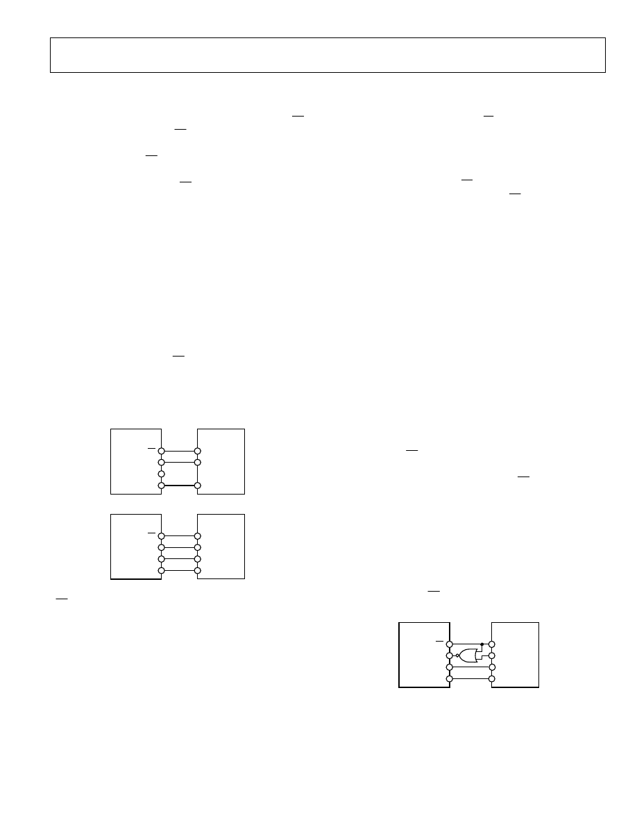
SPI
For SPI, either 3- or 4-wire configuration is possible, as shown in
the connection diagrams in Figure 34 and Figure 35. Clearing the
SPI bit (Bit D6) in the DATA_FORMAT register (Address 0x31)
selects 4-wire mode, whereas setting the SPI bit selects 3-wire
mode. The maximum SPI clock speed is 5 MHz with 100 pF
maximum loading, and the timing scheme follows clock polarity
(CPOL) = 1 and clock phase (CPHA) = 1. If power is applied to
the ADXL345 before the clock polarity and phase of the host
processor are configured, the CS pin should be brought high
before changing the clock polarity and phase. When using 3-wire
SPI, it is recommended that the SDO pin be either pulled up to
V
DD I/O
or pulled down to GND via a 10 kΩ resistor.
PROCESSOR
D OUT
D IN/OUT
D OUT
ADXL345
CS
SDIO
SDO
SCLK
07
92
5-
0
04
Figure 34. 3-Wire SPI Connection Diagram
PROCESSOR
D OUT
D OUT
D IN
D OUT
ADXL345
CS
SDI
SDO
SCLK
07
92
5-
00
3
Figure 35. 4-Wire SPI Connection Diagram
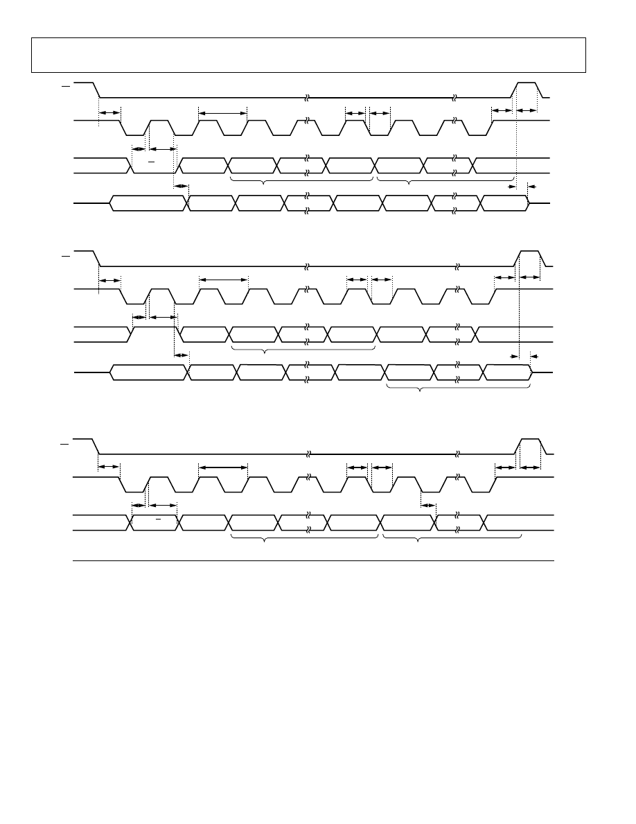
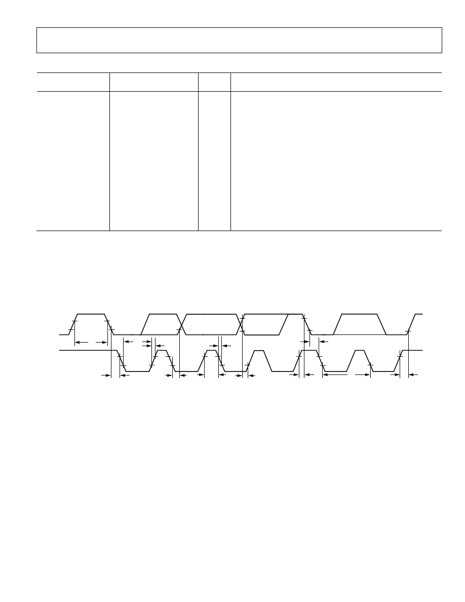
CS is the serial port enable line and is controlled by the SPI
master. This line must go low at the start of a transmission and
high at the end of a transmission, as shown in
. SCLK
is the serial port clock and is supplied by the SPI master. SCLK
should idle high during a period of no transmission. SDI and
SDO are the serial data input and output, respectively. Data is
updated on the falling edge of SCLK and should be sampled on
the rising edge of SCLK.
To read or write multiple bytes in a single transmission, the
multiple-byte bit, located after the R/W bit in the first byte transfer
(MB in
), must be set. After the register
addressing and the first byte of data, each subsequent set of
clock pulses (eight clock pulses) causes the ADXL345 to point
to the next register for a read or write. This shifting continues
until the clock pulses cease and
CS is deasserted. To perform reads or
writes on different, nonsequential registers, CS must be deasserted
between transmissions and the new register must be addressed
separately.
The timing diagram for 3-wire SPI reads or writes is shown
in Figure 39. The 4-wire equivalents for SPI writes and reads
are shown in Figure 37 and Figure 38, respectively. For correct
operation of the part, the logic thresholds and timing parameters
in Table 9 and Table 10 must be met at all times.
Use of the 3200 Hz and 1600 Hz output data rates is only
recommended with SPI communication rates greater than or
equal to 2 MHz. The 800 Hz output data rate is recommended
only for communication speeds greater than or equal to 400 kHz,
and the remaining data rates scale proportionally. For example,
the minimum recommended communication speed for a 200 Hz
output data rate is 100 kHz. Operation at an output data rate
above the recommended maximum may result in undesirable
effects on the acceleration data, including missing samples or
additional noise.
Preventing Bus Traffic Errors
The ADXL346 CS pin is used both for initiating SPI
transactions, and for enabling I
2
C mode. When the ADXL346 is
used on a SPI bus with multiple devices, its CS pin is held high
while the master communicates with the other devices. There
may be conditions where a SPI command transmitted to
another device looks like a valid I
2
C command. In this case, the
ADXL346 would interpret this as an attempt to communicate in
I
2
C mode, and could interfere with other bus traffic. Unless bus
traffic can be adequately controlled to assure such a condition
never occurs, it is recommended to add a logic gate in front of
the SDI pin as shown in
. This OR gate will hold the
SDA line high when
CS is high to prevent SPI bus traffic at the
ADXL346 from appearing as an I
2
C start command.
PROCESSOR
D OUT
D IN/OUT
D OUT
ADXL345
CS
SDIO
SDO
SCLK
07
92
5-
1
04
Figure 36. Recommended SPI Connection Diagram when Using Multiple SPI
Devices on a Single Bus
ADXL345
Rev. C | Page 16 of 40
07
92
5-
01
7
t
DELAY
t
SETUP
t
HOLD
t
SDO
X
X
X
W
MB
A5
A0
D7
D0
X
X
X
ADDRESS BITS
DATA BITS
t
SCLK
t
M
t
S
t
QUIET
t
DIS
t
CS,DIS
SCLK
SDI
SDO
CS
Figure 37. SPI 4-Wire Write
07
92
5-
01
8
CS
X
X
X
R
MB
A5
A0
D7
D0
X
X
X
ADDRESS BITS
DATA BITS
t
DIS
SCLK
SDI
SDO
t
QUIET
t
CS,DIS
t
SDO
t
SETUP
t
HOLD
t
DELAY
t
SCLK
t
M
t
S
Figure 38. SPI 4-Wire Read
07
92
5-
0
19
CS
t
DELAY
t
SETUP
t
HOLD
t
SDO
R/W
MB
A5
A0
D7
D0
ADDRESS BITS
DATA BITS
t
SCLK
t
M
t
S
t
QUIET
t
CS,DIS
SCLK
SDIO
SDO
NOTES
1.
t
SDO
IS ONLY PRESENT DURING READS.
Figure 39. SPI 3-Wire Read/Write
ADXL345
Rev. C | Page 17 of 40
Table 9. SPI Digital Input/Output
Parameter Test
Conditions
Min
Max
Unit
Digital Input
Low Level Input Voltage (V
IL
)
0.3
×
V
DD I/O
V
High Level Input Voltage (V
IH
)
0.7
×
V
DD I/O
V
Low Level Input Current (I
IL
) V
IN
= V
DD I/O
0.1
μA
High Level Input Current (I
IH
) V
IN
= 0 V
−0.1
μA
Digital Output
Low Level Output Voltage (V
OL
) I
OL
= 10 mA
0.2 × V
DD I/O
V
High Level Output Voltage (V
OH
) I
OH
= −4 mA
0.8 × V
DD I/O
V
Low Level Output Current (I
OL
) V
OL
= V
OL, max
10
mA
High Level Output Current (I
OH
) V
OH
= V
OH, min
−4
mA
Pin Capacitance
f
IN
= 1 MHz, V
IN
= 2.5 V
8
pF
1
Limits based on characterization results, not production tested.
Table 10. SPI Timing (T
A
= 25°C, V
S
= 2.5 V, V
DD I/O
= 1.8 V)
Parameter Min
Max
Unit
Description
f
SCLK
5
MHz
SPI clock frequency
t
SCLK
200
ns
1/(SPI clock frequency) mark-space ratio for the SCLK input is 40/60 to 60/40
t
DELAY
5
ns
CS falling edge to SCLK falling edge
t
QUIET
5
ns
SCLK rising edge to CS rising edge
t
DIS
10
ns
CS rising edge to SDO disabled
t
CS,DIS
150
ns
CS deassertion between SPI communications
t
S
0.3 × t
SCLK
ns
SCLK low pulse width (space)
t
M
0.3 × t
SCLK
ns
SCLK high pulse width (mark)
t
SETUP
5
ns
SDI valid before SCLK rising edge
t
HOLD
5
ns
SDI valid after SCLK rising edge
t
SDO
40
ns
SCLK falling edge to SDO/SDIO output transition
20
ns
SDO/SDIO output high to output low transition
20
ns
SDO/SDIO output low to output high transition
1
The CS, SCLK, SDI, and SDO pins are not internally pulled up or down; they must be driven for proper operation.
2
Limits based on characterization results, characterized with f
SCLK
= 5 MHz and bus load capacitance of 100 pF; not production tested.
3
The timing values are measured corresponding to the input thresholds (V
IL
and V
IH
4
Output rise and fall times measured with capacitive load of 150 pF.
ADXL345
Rev. C | Page 18 of 40
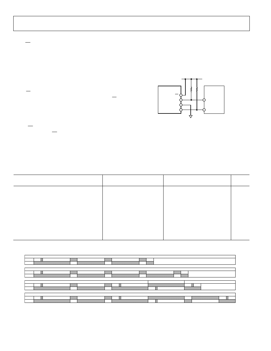
I
2
C
With CS tied high to V
DD I/O
, the ADXL345 is in I
2
C mode,
requiring a simple 2-wire connection, as shown in
.
The ADXL345 conforms to the UM10204 I
2
C-Bus Specification
and User Manual, Rev. 03—19 June 2007, available from NXP
Semiconductor. It supports standard (100 kHz) and fast (400 kHz)
data transfer modes if the bus parameters given in
and
are met. Single- or multiple-byte reads/writes are
. With the ALT ADDRESS pin
high, the 7-bit I
2
C address for the device is 0x1D, followed by
the R/
W bit. This translates to 0x3A for a write and 0x3B for a
read. An alternate I
2
C address of 0x53 (followed by the R/W bit)
can be chosen by grounding the ALT ADDRESS pin (Pin 12).
This translates to 0xA6 for a write and 0xA7 for a read.
There are no internal pull-up or pull-down resistors for any
unused pins; therefore, there is no known state or default state
for the CS or ALT ADDRESS pin if left floating or unconnected.
It is required that the CS pin be connected to V
DD I/O
and that
the ALT ADDRESS pin be connected to either V
DD I/O
or GND
when using I
2
C.
Due to communication speed limitations, the maximum output
data rate when using 400 kHz I
2
C is 800 Hz and scales linearly
with a change in the I
2
C communication speed. For example,
using I
2
C at 100 kHz would limit the maximum ODR to 200 Hz.
Operation at an output data rate above the recommended maxi-
mum may result in undesirable effect on the acceleration data,
including missing samples or additional noise.
PROCESSOR
D IN/OUT
D OUT
R
P
V
DD I/O
R
P
ADXL345
CS
SDA
ALT ADDRESS
SCL
07
92
5-
0
08
Figure 40. I
2
C Connection Diagram (Address 0x53)
If other devices are connected to the same I
2
C bus, the nominal
operating voltage level of these other devices cannot exceed V
DD I/O
by more than 0.3 V. External pull-up resistors, R
P
, are necessary for
proper I
2
C operation. Refer to the UM10204 I
2
C-Bus Specification
and User Manual, Rev. 03—19 June 2007, when selecting pull-up
resistor values to ensure proper operation.
Table 11. I
2
C Digital Input/Output
Parameter Test
Conditions
Min
Max
Unit
Digital Input
Low Level Input Voltage (V
IL
)
0.3
×
V
DD I/O
V
High Level Input Voltage (V
IH
)
0.7
×
V
DD I/O
V
Low Level Input Current (I
IL
) V
IN
= V
DD I/O
0.1
μA
High Level Input Current (I
IH
) V
IN
= 0 V
−0.1
μA
Digital Output
Low Level Output Voltage (V
OL
) V
DD I/O
< 2 V, I
OL
= 3 mA
0.2 × V
DD I/O
V
V
DD I/O
≥ 2 V, I
OL
= 3 mA
400
mV
Low Level Output Current (I
OL
) V
OL
= V
OL, max
3
mA
Pin Capacitance
f
IN
= 1 MHz, V
IN
= 2.5 V
8
pF
1
Limits based on characterization results; not production tested.
NOTES
1. THIS START IS EITHER A RESTART OR A STOP FOLLOWED BY A START.
2. THE SHADED AREAS REPRESENT WHEN THE DEVICE IS LISTENING.
MASTER START
SLAVE ADDRESS + WRITE
REGISTER ADDRESS
SLAVE
ACK
ACK
ACK
MASTER START
SLAVE ADDRESS + WRITE
REGISTER ADDRESS
SLAVE
ACK
ACK
ACK
ACK
MASTER START
SLAVE ADDRESS + WRITE
REGISTER ADDRESS
STOP
SLAVE
ACK
ACK
MASTER START
START
1
START
1
SLAVE ADDRESS + WRITE
REGISTER ADDRESS
NACK
STOP
SLAVE
ACK
ACK
DATA
STOP
ACK
SINGLE-BYTE WRITE
MULTIPLE-BYTE WRITE
DATA
DATA
MULTIPLE-BYTE READ
SLAVE ADDRESS + READ
SLAVE ADDRESS + READ
ACK
DATA
DATA
DATA
STOP
NACK
ACK
SINGLE-BYTE READ
07
92
5-
03
3
Figure 41. I
2
C Device Addressing
ADXL345
Rev. C | Page 19 of 40
Table 12. I
2
C Timing (T
A
= 25°C, V
S
= 2.5 V, V
DD I/O
= 1.8 V)
Parameter Min
Max
Unit
Description
f
SCL
400
kHz
SCL clock frequency
t
1
2.5
μs
SCL cycle time
t
2
0.6
μs
t
HIGH
, SCL high time
t
3
1.3
μs
t
LOW
, SCL low time
t
4
0.6
μs
t
HD, STA
, start/repeated start condition hold time
t
5
100
ns
t
SU, DAT
, data setup time
t
6
0
0.9
μs
t
HD, DAT
, data hold time
t
7
0.6
μs
t
SU, STA
, setup time for repeated start
t
8
0.6
μs
t
SU, STO
, stop condition setup time
t
9
1.3
μs
t
BUF
, bus-free time between a stop condition and a start condition
t
10
300
ns
t
R
, rise time of both SCL and SDA when receiving
0
ns
t
R
, rise time of both SCL and SDA when receiving or transmitting
t
11
300
ns
t
F
, fall time of SDA when receiving
250
ns
t
F
, fall time of both SCL and SDA when transmitting
C
b
400
pF
Capacitive load for each bus line
1
Limits based on characterization results, with f
SCL
= 400 kHz and a 3 mA sink current; not production tested.
2
All values referred to the V
IH
and the V
IL
3
t
6
is the data hold time that is measured from the falling edge of SCL. It applies to data in transmission and acknowledge.
4
A transmitting device must internally provide an output hold time of at least 300 ns for the SDA signal (with respect to V
IH(min)
of the SCL signal) to bridge the
undefined region of the falling edge of SCL.
5
The maximum t
6
value must be met only if the device does not stretch the low period (t
3
) of the SCL signal.
6
The maximum value for t
6
is a function of the clock low time (t
3
), the clock rise time (t
10
), and the minimum data setup time (t
5(min)
). This value is calculated as
t
6(max)
= t
3
− t
10
− t
5(min)
.
SDA
t
9
SCL
t
3
t
10
t
11
t
4
t
4
t
6
t
2
t
5
t
7
t
1
t
8
START
CONDITION
REPEATED
START
CONDITION
STOP
CONDITION
07
92
5-
0
34
Figure 42. I
2
C Timing Diagram

ADXL345
Rev. C | Page 20 of 40
INTERRUPTS
The ADXL345 provides two output pins for driving interrupts:
INT1 and INT2. Both interrupt pins are push-pull, low impedance
pins with output specifications shown in Table 13. The default
configuration of the interrupt pins is active high. This can be
changed to active low by setting the INT_INVERT bit in the
DATA_FORMAT (Address 0x31) register. All functions can
be used simultaneously, with the only limiting feature being
that some functions may need to share interrupt pins.
Interrupts are enabled by setting the appropriate bit in the
INT_ENABLE register (Address 0x2E) and are mapped to
either the INT1 pin or the INT2 pin based on the contents
of the INT_MAP register (Address 0x2F). When initially
configuring the interrupt pins, it is recommended that the
functions and interrupt mapping be done before enabling the
interrupts. When changing the configuration of an interrupt, it
is recommended that the interrupt be disabled first, by clearing
the bit corresponding to that function in the INT_ENABLE
register, and then the function be reconfigured before enabling
the interrupt again. Configuration of the functions while the
interrupts are disabled helps to prevent the accidental generation
of an interrupt before desired.
The interrupt functions are latched and cleared by either reading the
data registers (Address 0x32 to Address 0x37) until the interrupt
condition is no longer valid for the data-related interrupts or by
reading the INT_SOURCE register (Address 0x30) for the
remaining interrupts. This section describes the interrupts
that can be set in the INT_ENABLE register and monitored
in the INT_SOURCE register.
DATA_READY
The DATA_READY bit is set when new data is available and is
cleared when no new data is available.
SINGLE_TAP
The SINGLE_TAP bit is set when a single acceleration event
that is greater than the value in the THRESH_TAP register
(Address 0x1D) occurs for less time than is specified in the
DUR register (Address 0x21).
DOUBLE_TAP
The DOUBLE_TAP bit is set when two acceleration events
that are greater than the value in the THRESH_TAP register
(Address 0x1D) occur for less time than is specified in the DUR
register (Address 0x21), with the second tap starting after the
time specified by the latent register (Address 0x22) but within
the time specified in the window register (Address 0x23). See
the Tap Detection section for more details.
Activity
The activity bit is set when acceleration greater than the value stored
in the THRESH_ACT register (Address 0x24) is experienced on
any participating axis, set by the ACT_INACT_CTL register
(Address 0x27).
Inactivity
The inactivity bit is set when acceleration of less than the
value stored in the THRESH_INACT register (Address 0x25) is
experienced for more time than is specified in the TIME_INACT
register (Address 0x26) on all participating axes, as set by the
ACT_INACT_CTL register (Address 0x27). The maximum value
for TIME_INACT is 255 sec.
FREE_FALL
The FREE_FALL bit is set when acceleration of less than the
value stored in the THRESH_FF register (Address 0x28) is
experienced for more time than is specified in the TIME_FF
register (Address 0x29) on all axes (logical AND). The FREE_FALL
interrupt differs from the inactivity interrupt as follows: all axes
always participate and are logically AND’ed, the timer period is
much smaller (1.28 sec maximum), and the mode of operation is
always dc-coupled.
Watermark
The watermark bit is set when the number of samples in FIFO
equals the value stored in the samples bits (Register FIFO_CTL,
Address 0x38). The watermark bit is cleared automatically when
FIFO is read, and the content returns to a value below the value
stored in the samples bits.
Table 13. Interrupt Pin Digital Output
Parameter Test
Conditions
Min
Max
Unit
Digital
Output
Low Level Output Voltage (V
OL
) I
OL
= 300 μA
0.2 × V
DD I/O
V
High Level Output Voltage (V
OH
) I
OH
= −150 μA
0.8 × V
DD I/O
V
Low Level Output Current (I
OL
) V
OL
= V
OL, max
300
μA
High Level Output Current (I
OH
) V
OH
= V
OH, min
−150
μA
Pin Capacitance
f
IN
= 1 MHz, V
IN
= 2.5 V
8
pF
Rise/Fall
Time
Rise Time (t
C
LOAD
= 150 pF
210
ns
Fall Time (t
C
LOAD
= 150 pF
150
ns
1
Limits based on characterization results, not production tested.
2
Rise time is measured as the transition time from V
OL, max
to V
OH, min
of the interrupt pin.
3
Fall time is measured as the transition time from V
OH, min
to V
OL, max
of the interrupt pin.

ADXL345
Rev. C | Page 21 of 40
Overrun
The overrun bit is set when new data replaces unread data. The
precise operation of the overrun function depends on the FIFO
mode. In bypass mode, the overrun bit is set when new data replaces
unread data in the DATAX, DATAY, and DATAZ registers (Address
0x32 to Address 0x37). In all other modes, the overrun bit is set
when FIFO is filled. The overrun bit is automatically cleared when
the contents of FIFO are read.
FIFO
The ADXL345 contains patent pending technology for an
embedded memory management system with 32-level FIFO
that can be used to minimize host processor burden. This buffer
has four modes: bypass, FIFO, stream, and trigger (see FIFO
Modes). Each mode is selected by the settings of the
FIFO_MODE bits (Bits[D7:D6]) in the FIFO_CTL register
(Address 0x38).
Bypass Mode
In bypass mode, FIFO is not operational and, therefore,
remains empty.
FIFO Mode
In FIFO mode, data from measurements of the x-, y-, and z-axes
are stored in FIFO. When the number of samples in FIFO equals
the level specified in the samples bits of the FIFO_CTL register
(Address 0x38), the watermark interrupt is set. FIFO continues
accumulating samples until it is full (32 samples from measurements
of the x-, y-, and z-axes) and then stops collecting data. After FIFO
stops collecting data, the device continues to operate; therefore,
features such as tap detection can be used after FIFO is full. The
watermark interrupt continues to occur until the number of
samples in FIFO is less than the value stored in the samples bits
of the FIFO_CTL register.
Stream Mode
In stream mode, data from measurements of the x-, y-, and z-
axes are stored in FIFO. When the number of samples in FIFO
equals the level specified in the samples bits of the FIFO_CTL
register (Address 0x38), the watermark interrupt is set. FIFO
continues accumulating samples and holds the latest 32 samples
from measurements of the x-, y-, and z-axes, discarding older
data as new data arrives. The watermark interrupt continues
occurring until the number of samples in FIFO is less than the
value stored in the samples bits of the FIFO_CTL register.
Trigger Mode
In trigger mode, FIFO accumulates samples, holding the latest
32 samples from measurements of the x-, y-, and z-axes. After
a trigger event occurs and an interrupt is sent to the INT1 or
INT2 pin (determined by the trigger bit in the FIFO_CTL register),
FIFO keeps the last n samples (where n is the value specified by
the samples bits in the FIFO_CTL register) and then operates in
FIFO mode, collecting new samples only when FIFO is not full.
A delay of at least 5 μs should be present between the trigger event
occurring and the start of reading data from the FIFO to allow
the FIFO to discard and retain the necessary samples. Additional
trigger events cannot be recognized until the trigger mode is
reset. To reset the trigger mode, set the device to bypass mode
and then set the device back to trigger mode. Note that the FIFO
data should be read first because placing the device into bypass
mode clears FIFO.
Retrieving Data from FIFO
The FIFO data is read through the DATAX, DATAY, and DATAZ
registers (Address 0x32 to Address 0x37). When the FIFO is in
FIFO, stream, or trigger mode, reads to the DATAX, DATAY,
and DATAZ registers read data stored in the FIFO. Each time
data is read from the FIFO, the oldest x-, y-, and z-axes data are
placed into the DATAX, DATAY and DATAZ registers.
If a single-byte read operation is performed, the remaining
bytes of data for the current FIFO sample are lost. Therefore, all
axes of interest should be read in a burst (or multiple-byte) read
operation. To ensure that the FIFO has completely popped (that
is, that new data has completely moved into the DATAX, DATAY,
and DATAZ registers), there must be at least 5 μs between the
end of reading the data registers and the start of a new read of
the FIFO or a read of the FIFO_STATUS register (Address 0x39).
The end of reading a data register is signified by the transition
from Register 0x37 to Register 0x38 or by the CS pin going high.
For SPI operation at 1.6 MHz or less, the register addressing
portion of the transmission is a sufficient delay to ensure that
the FIFO has completely popped. For SPI operation greater than
1.6 MHz, it is necessary to deassert the CS pin to ensure a total
delay of 5 μs; otherwise, the delay is not sufficient. The total delay
necessary for 5 MHz operation is at most 3.4 μs. This is not a
concern when using I
2
C mode because the communication rate is
low enough to ensure a sufficient delay between FIFO reads.
ADXL345
Rev. C | Page 22 of 40
SELF-TEST
Table 14. Self-Test Output Scale Factors for Different Supply
Voltages, V
S
Supply Voltage, V
S
(V)
X-Axis, Y-Axis
The ADXL345 incorporates a self-test feature that effectively
tests its mechanical and electronic systems simultaneously.
When the self-test function is enabled (via the SELF_TEST bit
in the DATA_FORMAT register, Address 0x31), an electrostatic
force is exerted on the mechanical sensor. This electrostatic force
moves the mechanical sensing element in the same manner as
acceleration, and it is additive to the acceleration experienced
by the device. This added electrostatic force results in an output
change in the x-, y-, and z-axes. Because the electrostatic force
is proportional to V
S
2
, the output change varies with V
S
. This
effect is shown in Figure 43. The scale factors shown in Table 14
can be used to adjust the expected self-test output limits for
different supply voltages, V
S
. The self-test feature of the ADXL345
also exhibits a bimodal behavior. However, the limits shown in
Table 1 and Table 15 to Table 18 are valid for both potential self-
test values due to bimodality. Use of the self-test feature at data
rates less than 100 Hz or at 1600 Hz may yield values outside
these limits. Therefore, the part must be in normal power operation
(LOW_POWER bit = 0 in BW_RATE register, Address 0x2C)
and be placed into a data rate of 100 Hz through 800 Hz or 3200 Hz
for the self-test function to operate correctly.
Z-Axis
2.00 0.64
0.8
2.50 1.00
1.00
3.30 1.77
1.47
3.60 2.11
1.69
Table 15. Self-Test Output in LSB for ±2 g, 10-Bit or Full
Resolution (T
A
= 25°C, V
S
= 2.5 V, V
DD I/O
= 1.8 V)
Axis Min Max Unit
X 50 540 LSB
Y −540
−540
LSB
Z 75 875 LSB
Table 16. Self-Test Output in LSB for ±4 g, 10-Bit Resolution
(T
A
= 25°C, V
S
= 2.5 V, V
DD I/O
= 1.8 V)
Axis Min Max
Unit
X 25 270
LSB
Y −270
−25
LSB
Z 38 438
LSB
Table 17. Self-Test Output in LSB for ±8 g, 10-Bit Resolution
(T
A
= 25°C, V
S
= 2.5 V, V
DD I/O
= 1.8 V)
Axis Min Max
–6
–4
–2
0
2
4
6
2.0
2.5
3.3
3.6
V
S
(V)
SE
L
F
-T
EST
SH
IF
T
L
IM
IT
(g
)
X HIGH
X LOW
Y HIGH
Y LOW
Z HIGH
Z LOW
07
92
5-
24
2
Unit
X 12 135
LSB
Y −135
−12
LSB
Z 19 219
LSB
Table 18. Self-Test Output in LSB for ±16 g, 10-Bit Resolution
(T
A
= 25°C, V
S
= 2.5 V, V
DD I/O
= 1.8 V)
Axis Min Max
Unit
X 6 67
LSB
Y −67
−6
LSB
Z 10 110
LSB
Figure 43. Self-Test Output Change Limits vs. Supply Voltage
ADXL345
Rev. C | Page 23 of 40
REGISTER MAP
Table 19.
Address
Hex Dec
Name
Type
Reset
Value
Description
0x00 0
DEVID
R
11100101
Device
ID
0x01 to 0x1C
1 to 28
Reserved
Reserved; do not access
0x1D 29
THRESH_TAP
R/W
00000000 Tap
threshold
0x1E 30
OFSX
R/W
00000000 X-axis
offset
0x1F 31
OFSY
R/W
00000000 Y-axis
offset
0x20 32
OFSZ
R/W
00000000 Z-axis
offset
0x21 33
DUR
R/W
00000000 Tap
duration
0x22 34
Latent
R/W
00000000 Tap
latency
0x23 35
Window
R/W
00000000 Tap
window
0x24 36
THRESH_ACT
R/W
00000000 Activity
threshold
0x25 37
THRESH_INACT
R/W
00000000 Inactivity
threshold
0x26 38
TIME_INACT
R/W
00000000 Inactivity
time
0x27 39
ACT_INACT_CTL
R/W
00000000
Axis enable control for activity and inactivity detection
0x28 40
THRESH_FF R/W
00000000 Free-fall
threshold
0x29 41
TIME_FF R/W
00000000 Free-fall
time
0x2A 42
TAP_AXES R/W
00000000
Axis control for single tap/double tap
0x2B 43
ACT_TAP_STATUS
R
00000000
Source of single tap/double tap
0x2C 44
BW_RATE R/W
00001010
Data rate and power mode control
0x2D 45
POWER_CTL
R/W
00000000
Power-saving features control
0x2E 46
INT_ENABLE
R/W
00000000
Interrupt enable control
0x2F 47
INT_MAP R/W
00000000
Interrupt mapping control
0x30
48
INT_SOURCE
R
00000010
Source of interrupts
0x31 49
DATA_FORMAT
R/W
00000000
Data format control
0x32
50
DATAX0
R
00000000
X-Axis Data 0
0x33
51
DATAX1
R
00000000
X-Axis Data 1
0x34
52
DATAY0
R
00000000
Y-Axis Data 0
0x35
53
DATAY1
R
00000000
Y-Axis Data 1
0x36
54
DATAZ0
R
00000000
Z-Axis Data 0
0x37
55
DATAZ1
R
00000000
Z-Axis Data 1
0x38 56
FIFO_CTL R/W
00000000 FIFO
control
0x39 57
FIFO_STATUS
R
00000000
FIFO
status

ADXL345
Rev. C | Page 24 of 40
REGISTER DEFINITIONS
Register 0x00—DEVID (Read Only)
D7 D6 D5 D4 D3 D2 D1 D0
1 1 1 0 0 1 0 1
The DEVID register holds a fixed device ID code of 0xE5 (345 octal).
Register 0x1D—THRESH_TAP (Read/Write)
The THRESH_TAP register is eight bits and holds the threshold
value for tap interrupts. The data format is unsigned, therefore,
the magnitude of the tap event is compared with the value
in THRESH_TAP for normal tap detection. The scale factor is
62.5 mg/LSB (that is, 0xFF = 16 g). A value of 0 may result in
undesirable behavior if single tap/double tap interrupts are
enabled.
Register 0x1E, Register 0x1F, Register 0x20—OFSX,
OFSY, OFSZ (Read/Write)
The OFSX, OFSY, and OFSZ registers are each eight bits and
offer user-set offset adjustments in twos complement format
with a scale factor of 15.6 mg/LSB (that is, 0x7F = 2 g). The
value stored in the offset registers is automatically added to the
acceleration data, and the resulting value is stored in the output
data registers. For additional information regarding offset
calibration and the use of the offset registers, refer to the Offset
Calibration section.
Register 0x21—DUR (Read/Write)
The DUR register is eight bits and contains an unsigned time
value representing the maximum time that an event must be
above the THRESH_TAP threshold to qualify as a tap event. The
scale factor is 625 μs/LSB. A value of 0 disables the single tap/
double tap functions.
Register 0x22—Latent (Read/Write)
The latent register is eight bits and contains an unsigned time
value representing the wait time from the detection of a tap
event to the start of the time window (defined by the window
register) during which a possible second tap event can be detected.
The scale factor is 1.25 ms/LSB. A value of 0 disables the double tap
function.
Register 0x23—Window (Read/Write)
The window register is eight bits and contains an unsigned time
value representing the amount of time after the expiration of the
latency time (determined by the latent register) during which a
second valid tap can begin. The scale factor is 1.25 ms/LSB. A
value of 0 disables the double tap function.
Register 0x24—THRESH_ACT (Read/Write)
The THRESH_ACT register is eight bits and holds the threshold
value for detecting activity. The data format is unsigned, so the
magnitude of the activity event is compared with the value in
the THRESH_ACT register. The scale factor is 62.5 mg/LSB.
A value of 0 may result in undesirable behavior if the activity
interrupt is enabled.
Register 0x25—THRESH_INACT (Read/Write)
The THRESH_INACT register is eight bits and holds the threshold
value for detecting inactivity. The data format is unsigned, so
the magnitude of the inactivity event is compared with the value
in the THRESH_INACT register. The scale factor is 62.5 mg/LSB.
A value of 0 may result in undesirable behavior if the inactivity
interrupt is enabled.
Register 0x26—TIME_INACT (Read/Write)
The TIME_INACT register is eight bits and contains an unsigned
time value representing the amount of time that acceleration
must be less than the value in the THRESH_INACT register for
inactivity to be declared. The scale factor is 1 sec/LSB. Unlike
the other interrupt functions, which use unfiltered data (see the
Threshold section), the inactivity function uses filtered output
data. At least one output sample must be generated for the
inactivity interrupt to be triggered. This results in the function
appearing unresponsive if the TIME_INACT register is set to a
value less than the time constant of the output data rate. A value
of 0 results in an interrupt when the output data is less than the
value in the THRESH_INACT register.
Register 0x27—ACT_INACT_CTL (Read/Write)
D7 D6
D5
D4
ACT ac/dc
ACT_X enable
ACT_Y enable
ACT_Z enable
D3
D2
D1
D0
INACT ac/dc
INACT_X enable
INACT_Y enable
INACT_Z enable
ACT AC/DC and INACT AC/DC Bits
A setting of 0 selects dc-coupled operation, and a setting of 1
enables ac-coupled operation. In dc-coupled operation, the
current acceleration magnitude is compared directly with
THRESH_ACT and THRESH_INACT to determine whether
activity or inactivity is detected.
In ac-coupled operation for activity detection, the acceleration
value at the start of activity detection is taken as a reference
value. New samples of acceleration are then compared to this
reference value, and if the magnitude of the difference exceeds
the THRESH_ACT value, the device triggers an activity interrupt.
Similarly, in ac-coupled operation for inactivity detection, a
reference value is used for comparison and is updated whenever
the device exceeds the inactivity threshold. After the reference
value is selected, the device compares the magnitude of the
difference between the reference value and the current acceleration
with THRESH_INACT. If the difference is less than the value in
THRESH_INACT for the time in TIME_INACT, the device is
considered inactive and the inactivity interrupt is triggered.

ADXL345
Rev. C | Page 25 of 40
ACT_x Enable Bits and INACT_x Enable Bits
A setting of 1 enables x-, y-, or z-axis participation in detecting
activity or inactivity. A setting of 0 excludes the selected axis from
participation. If all axes are excluded, the function is disabled.
For activity detection, all participating axes are logically OR’ed,
causing the activity function to trigger when any of the partici-
pating axes exceeds the threshold. For inactivity detection, all
participating axes are logically AND’ed, causing the inactivity
function to trigger only if all participating axes are below the
threshold for the specified time.
Register 0x28—THRESH_FF (Read/Write)
The THRESH_FF register is eight bits and holds the threshold
value, in unsigned format, for free-fall detection. The acceleration on
all axes is compared with the value in THRESH_FF to determine if
a free-fall event occurred. The scale factor is 62.5 mg/LSB. Note
that a value of 0 mg may result in undesirable behavior if the free-
fall interrupt is enabled. Values between 300 mg and 600 mg
(0x05 to 0x09) are recommended.
Register 0x29—TIME_FF (Read/Write)
The TIME_FF register is eight bits and stores an unsigned time
value representing the minimum time that the value of all axes
must be less than THRESH_FF to generate a free-fall interrupt.
The scale factor is 5 ms/LSB. A value of 0 may result in undesirable
behavior if the free-fall interrupt is enabled. Values between 100 ms
and 350 ms (0x14 to 0x46) are recommended.
Register 0x2A—TAP_AXES (Read/Write)
D7 D6 D5 D4 D3
D2 D1 D0
0 0 0 0 Suppress
TAP_X
enable
TAP_Y
enable
TAP_Z
enable
Suppress Bit
Setting the suppress bit suppresses double tap detection if
acceleration greater than the value in THRESH_TAP is present
between taps. See the Tap Detection section for more details.
TAP_x Enable Bits
A setting of 1 in the TAP_X enable, TAP_Y enable, or TAP_Z
enable bit enables x-, y-, or z-axis participation in tap detection.
A setting of 0 excludes the selected axis from participation in
tap detection.
Register 0x2B—ACT_TAP_STATUS (Read Only)
D7
D6 D5 D4 D3 D2 D1 D0
0 ACT_X
source
ACT_Y
source
ACT_Z
source
Asleep TAP_X
source
TAP_Y
source
TAP_Z
source
ACT_x Source and TAP_x Source Bits
These bits indicate the first axis involved in a tap or activity
event. A setting of 1 corresponds to involvement in the event,
and a setting of 0 corresponds to no involvement. When new
data is available, these bits are not cleared but are overwritten by
the new data. The ACT_TAP_STATUS register should be read
before clearing the interrupt. Disabling an axis from participation
clears the corresponding source bit when the next activity or
single tap/double tap event occurs.
Asleep Bit
A setting of 1 in the asleep bit indicates that the part is asleep,
and a setting of 0 indicates that the part is not asleep. This bit
toggles only if the device is configured for auto sleep. See the
AUTO_SLEEP Bit section for more information on autosleep
mode.
Register 0x2C—BW_RATE (Read/Write)
D7 D6 D5 D4
D3 D2 D1 D0
0 0 0 LOW_POWER
Rate
LOW_POWER Bit
A setting of 0 in the LOW_POWER bit selects normal operation,
and a setting of 1 selects reduced power operation, which has
somewhat higher noise (see the Power Modes section for details).
Rate Bits
These bits select the device bandwidth and output data rate (see
Table 7 and Table 8 for details). The default value is 0x0A, which
translates to a 100 Hz output data rate. An output data rate should
be selected that is appropriate for the communication protocol
and frequency selected. Selecting too high of an output data rate with
a low communication speed results in samples being discarded.
Register 0x2D—POWER_CTL (Read/Write)
D7 D6 D5 D4
D3
D2
D1 D0
0 0 Link
AUTO_SLEEP
Measure
Sleep
Wakeup
Link Bit
A setting of 1 in the link bit with both the activity and inactivity
functions enabled delays the start of the activity function until
inactivity is detected. After activity is detected, inactivity detection
begins, preventing the detection of activity. This bit serially links
the activity and inactivity functions. When this bit is set to 0,
the inactivity and activity functions are concurrent. Additional
information can be found in the Link Mode section.
When clearing the link bit, it is recommended that the part be
placed into standby mode and then set back to measurement
mode with a subsequent write. This is done to ensure that the
device is properly biased if sleep mode is manually disabled;
otherwise, the first few samples of data after the link bit is cleared
may have additional noise, especially if the device was asleep
when the bit was cleared.
AUTO_SLEEP Bit
If the link bit is set, a setting of 1 in the AUTO_SLEEP bit enables
the auto-sleep functionality. In this mode, the ADXL345 auto-
matically switches to sleep mode if the inactivity function is
enabled and inactivity is detected (that is, when acceleration is
below the THRESH_INACT value for at least the time indicated
by TIME_INACT). If activity is also enabled, the ADXL345
automatically wakes up from sleep after detecting activity and
returns to operation at the output data rate set in the BW_RATE
register. A setting of 0 in the AUTO_SLEEP bit disables automatic
switching to sleep mode. See the description of the Sleep Bit in
this section for more information on sleep mode.
ADXL345
Rev. C | Page 26 of 40
If the link bit is not set, the AUTO_SLEEP feature is disabled
and setting the AUTO_SLEEP bit does not have an impact on
device operation. Refer to the Link Bit section or the Link Mode
section for more information on utilization of the link feature.
When clearing the AUTO_SLEEP bit, it is recommended that the
part be placed into standby mode and then set back to measure-
ment mode with a subsequent write. This is done to ensure that
the device is properly biased if sleep mode is manually disabled;
otherwise, the first few samples of data after the AUTO_SLEEP
bit is cleared may have additional noise, especially if the device
was asleep when the bit was cleared.
Measure Bit
A setting of 0 in the measure bit places the part into standby mode,
and a setting of 1 places the part into measurement mode. The
ADXL345 powers up in standby mode with minimum power
consumption.
Sleep Bit
A setting of 0 in the sleep bit puts the part into the normal mode
of operation, and a setting of 1 places the part into sleep mode.
Sleep mode suppresses DATA_READY, stops transmission of data
to FIFO, and switches the sampling rate to one specified by the
wakeup bits. In sleep mode, only the activity function can be used.
When the DATA_READY interrupt is suppressed, the output
data registers (Register 0x32 to Register 0x37) are still updated
at the sampling rate set by the wakeup bits (D1:D0).
When clearing the sleep bit, it is recommended that the part be
placed into standby mode and then set back to measurement
mode with a subsequent write. This is done to ensure that the
device is properly biased if sleep mode is manually disabled;
otherwise, the first few samples of data after the sleep bit is
cleared may have additional noise, especially if the device was
asleep when the bit was cleared.
Wakeup Bits
These bits control the frequency of readings in sleep mode as
described in Table 20.
Table 20. Frequency of Readings in Sleep Mode
Setting
D1 D0 Frequency
(Hz)
0 0 8
0 1 4
1 0 2
1 1 1
Register 0x2E—INT_ENABLE (Read/Write)
D7 D6
D5 D4
DATA_READY SINGLE_TAP DOUBLE_TAP Activity
D3
D2
D1
D0
Inactivity FREE_FALL
Watermark
Overrun
Setting bits in this register to a value of 1 enables their respective
functions to generate interrupts, whereas a value of 0 prevents
the functions from generating interrupts. The DATA_READY,
watermark, and overrun bits enable only the interrupt output;
the functions are always enabled. It is recommended that interrupts
be configured before enabling their outputs.
Register 0x2F—INT_MAP (R/W)
D7 D6
D5 D4
DATA_READY SINGLE_TAP DOUBLE_TAP Activity
D3
D2
D1
D0
Inactivity FREE_FALL
Watermark
Overrun
Any bits set to 0 in this register send their respective interrupts to
the INT1 pin, whereas bits set to 1 send their respective interrupts
to the INT2 pin. All selected interrupts for a given pin are OR’ed.
Register 0x30—INT_SOURCE (Read Only)
D7 D6
D5 D4
DATA_READY SINGLE_TAP DOUBLE_TAP Activity
D3
D2
D1
D0
Inactivity FREE_FALL
Watermark
Overrun
Bits set to 1 in this register indicate that their respective functions
have triggered an event, whereas a value of 0 indicates that the
corresponding event has not occurred. The DATA_READY,
watermark, and overrun bits are always set if the corresponding
events occur, regardless of the INT_ENABLE register settings,
and are cleared by reading data from the DATAX, DATAY, and
DATAZ registers. The DATA_READY and watermark bits may
require multiple reads, as indicated in the FIFO mode descriptions
in the FIFO section. Other bits, and the corresponding interrupts,
are cleared by reading the INT_SOURCE register.
Register 0x31—DATA_FORMAT (Read/Write)
D7
D6 D5
D4 D3
D2
D1 D0
SELF_TEST SPI INT_INVERT 0 FULL_RES Justify Range
The DATA_FORMAT register controls the presentation of data
to Register 0x32 through Register 0x37. All data, except that for
the ±16 g range, must be clipped to avoid rollover.
SELF_TEST Bit
A setting of 1 in the SELF_TEST bit applies a self-test force to
the sensor, causing a shift in the output data. A value of 0 disables
the self-test force.
SPI Bit
A value of 1 in the SPI bit sets the device to 3-wire SPI mode,
and a value of 0 sets the device to 4-wire SPI mode.
ADXL345
Rev. C | Page 27 of 40
INT_INVERT Bit
A value of 0 in the INT_INVERT bit sets the interrupts to active
high, and a value of 1 sets the interrupts to active low.
FULL_RES Bit
When this bit is set to a value of 1, the device is in full resolution
mode, where the output resolution increases with the g range
set by the range bits to maintain a 4 mg/LSB scale factor. When
the FULL_RES bit is set to 0, the device is in 10-bit mode, and
the range bits determine the maximum g range and scale factor.
Justify Bit
A setting of 1 in the justify bit selects left-justified (MSB) mode,
and a setting of 0 selects right-justified mode with sign extension.
Range Bits
These bits set the g range as described in Table 21.
Table 21. g Range Setting
Setting
D1 D0 g Range
0 0 ±2
g
0 1 ±4
g
1 0 ±8
g
1 1 ±16
g
Register 0x32 to Register 0x37—DATAX0, DATAX1,
DATAY0, DATAY1, DATAZ0, DATAZ1 (Read Only)
These six bytes (Register 0x32 to Register 0x37) are eight bits
each and hold the output data for each axis. Register 0x32 and
Register 0x33 hold the output data for the x-axis, Register 0x34 and
Register 0x35 hold the output data for the y-axis, and Register 0x36
and Register 0x37 hold the output data for the z-axis. The output
data is twos complement, with DATAx0 as the least significant
byte and DATAx1 as the most significant byte, where x represent X,
Y, or Z. The DATA_FORMAT register (Address 0x31) controls
the format of the data. It is recommended that a multiple-byte
read of all registers be performed to prevent a change in data
between reads of sequential registers.
Register 0x38—FIFO_CTL (Read/Write)
D7 D6 D5
D4 D3 D2 D1 D0
FIFO_MODE Trigger
Samples
FIFO_MODE Bits
These bits set the FIFO mode, as described in Table 22.
Table 22. FIFO Modes
Setting
D7 D6 Mode Function
0
0
Bypass
FIFO is bypassed.
0 1 FIFO FIFO collects up to 32 values and then
stops collecting data, collecting new data
only when FIFO is not full.
1 0 Stream
FIFO holds the last 32 data values. When
FIFO is full, the oldest data is overwritten
with newer data.
1 1 Trigger
When triggered by the trigger bit, FIFO
holds the last data samples before the
trigger event and then continues to collect
data until full. New data is collected only
when FIFO is not full.
Trigger Bit
A value of 0 in the trigger bit links the trigger event of trigger mode
to INT1, and a value of 1 links the trigger event to INT2.
Samples Bits
The function of these bits depends on the FIFO mode selected
(see Table 23). Entering a value of 0 in the samples bits
immediately sets the watermark status bit in the INT_SOURCE
register, regardless of which FIFO mode is selected. Undesirable
operation may occur if a value of 0 is used for the samples bits
when trigger mode is used.
Table 23. Samples Bits Functions
FIFO Mode
Samples Bits Function
Bypass None.
FIFO
Specifies how many FIFO entries are needed to
trigger a watermark interrupt.
Stream
Specifies how many FIFO entries are needed to
trigger a watermark interrupt.
Trigger
Specifies how many FIFO samples are retained in
the FIFO buffer before a trigger event.
0x39—FIFO_STATUS (Read Only)
D7
D6 D5 D4 D3 D2 D1 D0
FIFO_TRIG 0
Entries
FIFO_TRIG Bit
A 1 in the FIFO_TRIG bit corresponds to a trigger event occurring,
and a 0 means that a FIFO trigger event has not occurred.
Entries Bits
These bits report how many data values are stored in FIFO.
Access to collect the data from FIFO is provided through the
DATAX, DATAY, and DATAZ registers. FIFO reads must be
done in burst or multiple-byte mode because each FIFO level is
cleared after any read (single- or multiple-byte) of FIFO. FIFO
stores a maximum of 32 entries, which equates to a maximum
of 33 entries available at any given time because an additional
entry is available at the output filter of the device.
ADXL345
Rev. C | Page 28 of 40
APPLICATIONS INFORMATION
POWER SUPPLY DECOUPLING
A 1 μF tantalum capacitor (C
S
) at V
S
and a 0.1 μF ceramic capacitor
(C
I/O
) at V
DD I/O
placed close to the ADXL345 supply pins is
recommended to adequately decouple the accelerometer from
noise on the power supply. If additional decoupling is necessary,
a resistor or ferrite bead, no larger than 100 Ω, in series with V
S
may be helpful. Additionally, increasing the bypass capacitance
on V
S
to a 10 μF tantalum capacitor in parallel with a 0.1 μF
ceramic capacitor may also improve noise.
Care should be taken to ensure that the connection from the
ADXL345 ground to the power supply ground has low impedance
because noise transmitted through ground has an effect similar
to noise transmitted through V
S
. It is recommended that V
S
and
V
DD I/O
be separate supplies to minimize digital clocking noise
on the V
S
supply. If this is not possible, additional filtering of
the supplies, as previously mentioned, may be necessary.
07
92
5-
0
16
ADXL345
GND
INT1
INT2
CS
SCL/SCLK
SDO/ALT ADDRESS
SDA/SDI/SDIO
3- OR 4-WIRE
SPI OR I
2
C
INTERFACE
V
S
V
S
C
S
V
DD I/O
V
DD I/O
C
IO
INTERRUPT
CONTROL
Figure 44. Application Diagram
MECHANICAL CONSIDERATIONS FOR MOUNTING
The ADXL345 should be mounted on the PCB in a location
close to a hard mounting point of the PCB to the case. Mounting
the ADXL345 at an unsupported PCB location, as shown in
Figure 45, may result in large, apparent measurement errors
due to undampened PCB vibration. Locating the accelerometer
near a hard mounting point ensures that any PCB vibration at
the accelerometer is above the accelerometer’s mechanical sensor
resonant frequency and, therefore, effectively invisible to the
accelerometer. Multiple mounting points, close to the sensor,
and/or a thicker PCB also help to reduce the effect of system
resonance on the performance of the sensor.
MOUNTING POINTS
PCB
ACCELEROMETERS
0
79
25
-0
36
Figure 45. Incorrectly Placed Accelerometers
TAP DETECTION
The tap interrupt function is capable of detecting either single
or double taps. The following parameters are shown in Figure 46
for a valid single and valid double tap event:
• The tap detection threshold is defined by the THRESH_TAP
register (Address 0x1D).
• The maximum tap duration time is defined by the DUR
register (Address 0x21).
• The tap latency time is defined by the latent register
(Address 0x22) and is the waiting period from the end
of the first tap until the start of the time window, when a
second tap can be detected, which is determined by the
value in the window register (Address 0x23).
• The interval after the latency time (set by the latent register) is
defined by the window register. Although a second tap must
begin after the latency time has expired, it need not finish
before the end of the time defined by the window register.
FIRST TAP
TIME LIMIT FOR
TAPS (DUR)
LATENCY
TIME
(LATENT)
TIME WINDOW FOR
SECOND TAP (WINDOW)
SECOND TAP
SINGLE TAP
INTERRUPT
DOUBLE TAP
INTERRUPT
THRESHOLD
(THRESH_TAP)
X
HI
BW
INT
E
RRU
P
T
S
07
92
5-
0
37
Figure 46. Tap Interrupt Function with Valid Single and Double Taps
If only the single tap function is in use, the single tap interrupt
is triggered when the acceleration goes below the threshold, as
long as DUR has not been exceeded. If both single and double
tap functions are in use, the single tap interrupt is triggered
when the double tap event has been either validated or
invalidated.
ADXL345
Rev. C | Page 29 of 40
Several events can occur to invalidate the second tap of a double
tap event. First, if the suppress bit in the TAP_AXES register
(Address 0x2A) is set, any acceleration spike above the threshold
during the latency time (set by the latent register) invalidates
the double tap detection, as shown in Figure 47.
INVALIDATES DOUBLE TAP IF
SUPRESS BIT SET
TIME WINDOW FOR SECOND
TAP (WINDOW)
LATENCY
TIME (LATENT)
TIME LIMIT
FOR TAPS
(DUR)
X
HI
BW
07
92
5-
03
8
Figure 47. Double Tap Event Invalid Due to High g Event
When the Suppress Bit Is Set
A double tap event can also be invalidated if acceleration above
the threshold is detected at the start of the time window for the
second tap (set by the window register). This results in an invalid
double tap at the start of this window, as shown in Figure 48.
Additionally, a double tap event can be invalidated if an accel-
eration exceeds the time limit for taps (set by the DUR register),
resulting in an invalid double tap at the end of the DUR time
limit for the second tap event, also shown in Figure 48.
INVALIDATES DOUBLE TAP
AT START OF WINDOW
TIME WINDOW FOR
SECOND TAP (WINDOW)
LATENCY
TIME
(LATENT)
INVALIDATES
DOUBLE TAP AT
END OF DUR
TIME LIMIT
FOR TAPS
(DUR)
TIME LIMIT
FOR TAPS
(DUR)
TIME LIMIT
FOR TAPS
(DUR)
X
HI
B
W
X
HI
B
W
07
92
5-
0
39
Figure 48. Tap Interrupt Function with Invalid Double Taps
Single taps, double taps, or both can be detected by setting the
respective bits in the INT_ENABLE register (Address 0x2E).
Control over participation of each of the three axes in single tap/
double tap detection is exerted by setting the appropriate bits in
the TAP_AXES register (Address 0x2A). For the double tap
function to operate, both the latent and window registers must
be set to a nonzero value.
Every mechanical system has somewhat different single tap/
double tap responses based on the mechanical characteristics of
the system. Therefore, some experimentation with values for the
DUR, latent, window, and THRESH_TAP registers is required.
In general, a good starting point is to set the DUR register to a
value greater than 0x10 (10 ms), the latent register to a value greater
than 0x10 (20 ms), the window register to a value greater than
0x40 (80 ms), and the THRESH_TAP register to a value greater
than 0x30 (3 g). Setting a very low value in the latent, window, or
THRESH_TAP register may result in an unpredictable response
due to the accelerometer picking up echoes of the tap inputs.
After a tap interrupt has been received, the first axis to exceed
the THRESH_TAP level is reported in the ACT_TAP_STATUS
register (Address 0x2B). This register is never cleared but is
overwritten with new data.
THRESHOLD
The lower output data rates are achieved by decimating a common
sampling frequency inside the device. The activity, free-fall, and
single tap/double tap detection functions without improved tap
enabled are performed using undecimated data. Because the
bandwidth of the output data varies with the data rate and is
lower than the bandwidth of the undecimated data, the high
frequency and high g data that is used to determine activity,
free-fall, and single tap/double tap events may not be present
if the output of the accelerometer is examined. This may result
in functions triggering when acceleration data does not appear
to meet the conditions set by the user for the corresponding
function.
LINK MODE
The function of the link bit is to reduce the number of activity
interrupts that the processor must service by setting the device
to look for activity only after inactivity. For proper operation of
this feature, the processor must still respond to the activity and
inactivity interrupts by reading the INT_SOURCE register
(Address 0x30) and, therefore, clearing the interrupts. If an activity
interrupt is not cleared, the part cannot go into autosleep mode.
The asleep bit in the ACT_TAP_STATUS register (Address 0x2B)
indicates if the part is asleep.

ADXL345
Rev. C | Page 30 of 40
SLEEP MODE VS. LOW POWER MODE
In applications where a low data rate and low power consumption
is desired (at the expense of noise performance), it is recommended
that low power mode be used. The use of low power mode preserves
the functionality of the DATA_READY interrupt and the FIFO
for postprocessing of the acceleration data. Sleep mode, while
offering a low data rate and power consumption, is not intended
for data acquisition.
However, when sleep mode is used in conjunction with the
AUTO_SLEEP mode and the link mode, the part can automatically
switch to a low power, low sampling rate mode when inactivity
is detected. To prevent the generation of redundant inactivity
interrupts, the inactivity interrupt is automatically disabled
and activity is enabled. When the ADXL345 is in sleep mode, the
host processor can also be placed into sleep mode or low power
mode to save significant system power. When activity is detected,
the accelerometer automatically switches back to the original
data rate of the application and provides an activity interrupt
that can be used to wake up the host processor. Similar to when
inactivity occurs, detection of activity events is disabled and
inactivity is enabled.
OFFSET CALIBRATION
Accelerometers are mechanical structures containing elements
that are free to move. These moving parts can be very sensitive
to mechanical stresses, much more so than solid-state electronics.
The 0 g bias or offset is an important accelerometer metric because
it defines the baseline for measuring acceleration. Additional
stresses can be applied during assembly of a system containing
an accelerometer. These stresses can come from, but are not
limited to, component soldering, board stress during mounting,
and application of any compounds on or over the component. If
calibration is deemed necessary, it is recommended that calibration
be performed after system assembly to compensate for these effects.
A simple method of calibration is to measure the offset while
assuming that the sensitivity of the ADXL345 is as specified in
Table 1. The offset can then be automatically accounted for by
using the built-in offset registers. This results in the data acquired
from the DATA registers already compensating for any offset.
In a no-turn or single-point calibration scheme, the part is oriented
such that one axis, typically the z-axis, is in the 1 g field of gravity
and the remaining axes, typically the x- and y-axis, are in a 0 g
field. The output is then measured by taking the average of a
series of samples. The number of samples averaged is a choice of
the system designer, but a recommended starting point is 0.1 sec
worth of data for data rates of 100 Hz or greater. This corresponds
to 10 samples at the 100 Hz data rate. For data rates less than
100 Hz, it is recommended that at least 10 samples be averaged
together. These values are stored as X
0g
, Y
0g
, and Z
+1g
for the 0 g
measurements on the x- and y-axis and the 1 g measurement on
the z-axis, respectively.
The values measured for X
0g
and Y
0g
correspond to the x- and y-axis
offset, and compensation is done by subtracting those values from
the output of the accelerometer to obtain the actual acceleration:
X
ACTUAL
= X
MEAS
− X
0g
Y
ACTUAL
= Y
MEAS
− Y
0g
Because the z-axis measurement was done in a +1 g field, a no-turn
or single-point calibration scheme assumes an ideal sensitivity,
S
Z
for the z-axis. This is subtracted from Z
+1g
to attain the z-axis
offset, which is then subtracted from future measured values to
obtain the actual value:
Z
0g
= Z
+1g
− S
Z
Z
ACTUAL
= Z
MEAS
− Z
0g
The ADXL345 can automatically compensate the output for offset
by using the offset registers (Register 0x1E, Register 0x1F, and
Register 0x20). These registers contain an 8-bit, twos complement
value that is automatically added to all measured acceleration
values, and the result is then placed into the DATA registers.
Because the value placed in an offset register is additive, a negative
value is placed into the register to eliminate a positive offset and
vice versa for a negative offset. The register has a scale factor of
15.6 mg/LSB and is independent of the selected g-range.
As an example, assume that the ADXL345 is placed into full-
resolution mode with a sensitivity of typically 256 LSB/g. The
part is oriented such that the z-axis is in the field of gravity and
x-, y-, and z-axis outputs are measured as +10 LSB, −13 LSB,
and +9 LSB, respectively. Using the previous equations, X
0g
is
+10 LSB, Y
0g
is −13 LSB, and Z
0g
is +9 LSB. Each LSB of output
in full-resolution is 3.9 mg or one-quarter of an LSB of the
offset register. Because the offset register is additive, the 0 g
values are negated and rounded to the nearest LSB of the offset
register:
X
OFFSET
= −Round(10/4) = −3 LSB
Y
OFFSET
= −Round(−13/4) = 3 LSB
Z
OFFSET
= −Round(9/4) = −2 LSB
These values are programmed into the OFSX, OFSY, and OFXZ
registers, respectively, as 0xFD, 0x03 and 0xFE. As with all
registers in the ADXL345, the offset registers do not retain the
value written into them when power is removed from the part.
Power-cycling the ADXL345 returns the offset registers to their
default value of 0x00.
Because the no-turn or single-point calibration method assumes an
ideal sensitivity in the z-axis, any error in the sensitivity results in
offset error. For instance, if the actual sensitivity was 250 LSB/g
in the previous example, the offset would be 15 LSB, not 9 LSB.
To help minimize this error, an additional measurement point
can be used with the z-axis in a 0 g field and the 0 g measurement
can be used in the Z
ACTUAL
equation.

ADXL345
Rev. C | Page 31 of 40
USING SELF-TEST
The self-test change is defined as the difference between the
acceleration output of an axis with self-test enabled and the
acceleration output of the same axis with self-test disabled (see
Endnote 4 of Table 1). This definition assumes that the sensor
does not move between these two measurements, because if the
sensor moves, a non–self-test related shift corrupts the test.
Proper configuration of the ADXL345 is also necessary for an
accurate self-test measurement. The part should be set with a
data rate of 100 Hz through 800 Hz, or 3200 Hz. This is done by
ensuring that a value of 0x0A through 0x0D, or 0x0F is written
into the rate bits (Bit D3 through Bit D0) in the BW_RATE
register (Address 0x2C). The part also must be placed into
normal power operation by ensuring the LOW_POWER bit in
the BW_RATE register is cleared (LOW_POWER bit = 0) for
accurate self-test measurements. It is recommended that the
part be set to full-resolution, 16 g mode to ensure that there is
sufficient dynamic range for the entire self-test shift. This is done
by setting Bit D3 of the DATA_FORMAT register (Address 0x31)
and writing a value of 0x03 to the range bits (Bit D1 and Bit D0) of
the DATA_FORMAT register (Address 0x31). This results in a high
dynamic range for measurement and a 3.9 mg/LSB scale factor.
After the part is configured for accurate self-test measurement,
several samples of x-, y-, and z-axis acceleration data should be
retrieved from the sensor and averaged together. The number
of samples averaged is a choice of the system designer, but a
recommended starting point is 0.1 sec worth of data for data
rates of 100 Hz or greater. This corresponds to 10 samples at
the 100 Hz data rate. For data rates less than 100 Hz, it is
recommended that at least 10 samples be averaged together. The
averaged values should be stored and labeled appropriately as
the self-test disabled data, that is, X
ST_OFF
, Y
ST_OFF
, and Z
ST_OFF
.
Next, self-test should be enabled by setting Bit D7 (SELF_TEST) of
the DATA_FORMAT register (Address 0x31). The output needs
some time (about four samples) to settle after enabling self-test.
After allowing the output to settle, several samples of the x-, y-,
and z-axis acceleration data should be taken again and averaged. It
is recommended that the same number of samples be taken for
this average as was previously taken. These averaged values should
again be stored and labeled appropriately as the value with self-
test enabled, that is, X
ST_ON
, Y
ST_ON
, and Z
ST_ON
. Self-test can then be
disabled by clearing Bit D7 (SELF_TEST) of the DATA_FORMAT
register (Address 0x31).
With the stored values for self-test enabled and disabled, the
self-test change is as follows:
X
ST
= X
ST_ON
− X
ST_OFF
Y
ST
= Y
ST_ON
− Y
ST_OFF
Z
ST
= Z
ST_ON
− Z
ST_OFF
Because the measured output for each axis is expressed in LSBs,
X
ST
, Y
ST
, and Z
ST
are also expressed in LSBs. These values can be
converted to g’s of acceleration by multiplying each value by the
3.9 mg/LSB scale factor, if configured for full-resolution mode.
Additionally, Table 15 through Table 18 correspond to the self-test
range converted to LSBs and can be compared with the measured
self-test change when operating at a V
S
of 2.5 V. For other voltages,
the minimum and maximum self-test output values should be
adjusted based on (multiplied by) the scale factors shown in
Table 14. If the part was placed into ±2 g, 10-bit or full-resolution
mode, the values listed in Table 15 should be used. Although
the fixed 10-bit mode or a range other than 16 g can be used, a
different set of values, as indicated in Table 16 through Table 18,
would need to be used. Using a range below 8 g may result in
insufficient dynamic range and should be considered when
selecting the range of operation for measuring self-test.
If the self-test change is within the valid range, the test is considered
successful. Generally, a part is considered to pass if the minimum
magnitude of change is achieved. However, a part that changes
by more than the maximum magnitude is not necessarily a failure.
Another effective method for using the self-test to verify accel-
erometer functionality is to toggle the self test at a certain rate
and then perform an FFT on the output. The FFT should have a
corresponding tone at the frequency the self-test was toggled.
Using an FFT like this removes the dependency of the test on
supply voltage and on self-test magnitude, which can vary within
a rather wide range.
ADXL345
Rev. C | Page 32 of 40
DATA FORMATTING OF UPPER DATA RATES
For a range of ±2 g, the LSB is Bit D6 of the DATAx0 register;
for ±4 g, Bit D5 of the DATAx0 register; for ±8 g, Bit D4 of the
DATAx0 register; and for ±16 g, Bit D3 of the DATAx0 register.
This is shown in Figure 50.
Formatting of output data at the 3200 Hz and 1600 Hz output
data rates changes depending on the mode of operation (full-
resolution or fixed 10-bit) and the selected output range.
The use of 3200 Hz and 1600 Hz output data rates for fixed 10-
bit operation in the ±4 g, ±8 g, and ±16 g output ranges
provides an LSB that is valid and that changes according to the
applied acceleration. Therefore, in these modes of operation, Bit
D0 is not always 0 when output data is right justified and Bit D6
is not always 0 when output data is left justified. Operation at
any data rate of 800 Hz or lower also provides a valid LSB in all
ranges and modes that changes according to the applied
acceleration.
When using the 3200 Hz or 1600 Hz output data rates in full-
resolution or ±2 g, 10-bit operation, the LSB of the output data-
word is always 0. When data is right justified, this corresponds
to Bit D0 of the DATAx0 register, as shown in Figure 49. When
data is left justified and the part is operating in ±2 g, 10-bit mode,
the LSB of the output data-word is Bit D6 of the DATAx0 register.
In full-resolution operation when data is left justified, the location
of the LSB changes according to the selected output range.
0
D1
D2
D3
D4
D5
D6
D7
D0
D1
D2
D3
D4
D5
D6
D7
D0
D1
D2
D3
D4
D5
D6
D7
D0
D1
D2
D3
D4
D5
D6
D7
DATAx1 REGISTER
DATAx0 REGISTER
OUTPUT DATA-WORD FOR
±16g, FULL-RESOLUTION MODE.
OUTPUT DATA-WORD FOR ALL
10-BIT MODES AND THE ±2g,
FULL-RESOLUTION MODE.
THE ±4g AND ±8g FULL-RESOLUTION MODES HAVE THE SAME LSB LOCATION AS THE ±2g
AND ±16g FULL-RESOLUTION MODES, BUT THE MSB LOCATION CHANGES TO BIT D2 AND
BIT D3 OF THE DATAX1 REGISTER FOR ±4g AND ±8g, RESPECTIVELY.
07
92
5
-14
5
Figure 49. Data Formatting of Full-Resolution and ±2 g, 10-Bit Modes of Operation When Output Data Is Right Justified
0
D1
D2
D3
D4
D5
D6
D7
D0
D1
D2
D3
D4
D5
D6
D7
D0
D1
D2
D3
D4
D5
D6
D7
D0
D1
D2
D3
D4
D5
D6
D7
DATAx1 REGISTER
DATAx0 REGISTER
MSB FOR ALL MODES
OF OPERATION WHEN
LEFT JUSTIFIED.
LSB FOR ±2g, FULL-RESOLUTION
AND ±2g, 10-BIT MODES.
LSB FOR ±4g, FULL-RESOLUTION MODE.
LSB FOR ±8g, FULL-RESOLUTION MODE.
LSB FOR ±16g, FULL-RESOLUTION MODE.
FOR 3200Hz AND 1600Hz OUTPUT DATA RATES, THE LSB IN THESE MODES IS ALWAYS 0.
ADDITIONALLY, ANY BITS TO THE RIGHT OF THE LSB ARE ALWAYS 0 WHEN THE OUTPUT
DATA IS LEFT JUSTIFIED.
07
92
5-
14
6
Figure 50. Data Formatting of Full-Resolution and ±2 g, 10-Bit Modes of Operation When Output Data Is Left Justified
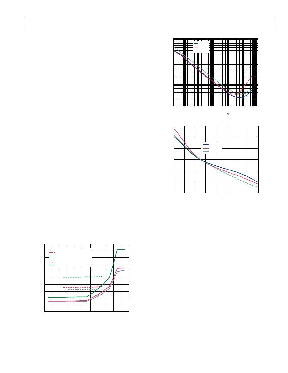
ADXL345
Rev. C | Page 33 of 40
NOISE PERFORMANCE
The specification of noise shown in Table 1 corresponds to
the typical noise performance of the ADXL345 in normal power
operation with an output data rate of 100 Hz (LOW_POWER bit
(D4) = 0, rate bits (D3:D0) = 0xA in the BW_RATE register,
Address 0x2C). For normal power operation at data rates below
100 Hz, the noise of the ADXL345 is equivalent to the noise at
100 Hz ODR in LSBs. For data rates greater than 100 Hz, the
noise increases roughly by a factor of √2 per doubling of the data
rate. For example, at 400 Hz ODR, the noise on the x- and y-axes
is typically less than 1.5 LSB rms, and the noise on the z-axis is
typically less than 2.2 LSB rms.
For low power operation (LOW_POWER bit (D4) = 1 in the
BW_RATE register, Address 0x2C), the noise of the ADXL345
is constant for all valid data rates shown in Table 8. This value is
typically less than 1.8 LSB rms for the x- and y-axes and typically
less than 2.6LSB rms for the z-axis.
The trend of noise performance for both normal power and low
power modes of operation of the ADXL345 is shown in Figure 51.
Figure 52 shows the typical Allan deviation for the ADXL345.
The 1/f corner of the device, as shown in this figure, is very low,
allowing absolute resolution of approximately 100 μg (assuming
that there is sufficient integration time). Figure 52 also shows
that the noise density is 290 μg/√Hz for the x-axis and y-axis
and 430 μg/√Hz for the z-axis.
Figure 53 shows the typical noise performance trend of the
ADXL345 over supply voltage. The performance is normalized
to the tested and specified supply voltage, V
S
= 2.5 V. In general,
noise decreases as supply voltage is increased. It should be noted, as
shown in Figure 51, that the noise on the z-axis is typically higher
than on the x-axis and y-axis; therefore, while they change roughly
the same in percentage over supply voltage, the magnitude of change
on the z-axis is greater than the magnitude of change on the
x-axis and y-axis.
0
0.5
1.0
1.5
2.0
2.5
3.0
3.5
4.0
4.5
5.0
3.13 6.25 12.50
25
50
100
200
400
800
1600 3200
OUTPUT DATA RATE (Hz)
O
UT
P
UT
NO
IS
E
(
L
S
B rm
s)
X-AXIS, NORMAL POWER
X-AXIS, LOW POWER
Y-AXIS, NORMAL POWER
Y-AXIS, LOW POWER
Z-AXIS, NORMAL POWER
Z-AXIS, LOW POWER
07
92
5-
2
50
Figure 51. Noise vs. Output Data Rate for Normal and Low Power Modes,
Full-Resolution (256 LSB/g)
0.01
0.1
1
10
100
1k
10k
10
100
1k
10k
AVERAGING PERIOD, (s)
A
L
L
AN DE
V
IA
TI
O
N
(
µ
g
)
X-AXIS
Y-AXIS
Z-AXIS
07
92
5-
25
1
Figure 52. Root Allan Deviation
70
80
90
100
110
120
130
2.0
2.2
2.4
2.6
2.8
3.0
3.2
3.4
3.6
SUPPLY VOLTAGE, V
S
(V)
P
E
R
CE
N
T
A
G
E
O
F
NO
RM
AL
IZ
E
D
N
O
IS
E
(
%
)
X-AXIS
Y-AXIS
Z-AXIS
07
92
5-
25
2
Figure 53. Normalized Noise vs. Supply Voltage, V
S
OPERATION AT VOLTAGES OTHER THAN 2.5 V
The ADXL345 is tested and specified at a supply voltage of
V
S
= 2.5 V; however, it can be powered with V
S
as high as 3.6 V
or as low as 2.0 V. Some performance parameters change as the
supply voltage changes: offset, sensitivity, noise, self-test, and
supply current.
Due to slight changes in the electrostatic forces as supply voltage
is varied, the offset and sensitivity change slightly. When operating
at a supply voltage of V
S
= 3.3 V, the x- and y-axis offset is typically
25 mg higher than at Vs = 2.5 V operation. The z-axis is typically
20 mg lower when operating at a supply voltage of 3.3 V than when
operating at V
S
= 2.5 V. Sensitivity on the x- and y-axes typically
shifts from a nominal 256 LSB/g (full-resolution or ±2 g, 10-bit
operation) at V
S
= 2.5 V operation to 265 LSB/g when operating
with a supply voltage of 3.3 V. The z-axis sensitivity is unaffected by
a change in supply voltage and is the same at V
S
= 3.3 V operation
as it is at V
S
= 2.5 V operation. Simple linear interpolation can be
used to determine typical shifts in offset and sensitivity at other
supply voltages.
ADXL345
Rev. C | Page 34 of 40
Changes in noise performance, self-test response, and supply
current are discussed elsewhere throughout the data sheet. For
noise performance, the Noise Performance section should be
reviewed. The Using Self-Test section discusses both the
operation of self-test over voltage, a square relationship with
supply voltage, as well as the conversion of the self-test response
in g’s to LSBs. Finally, Figure 33 shows the impact of supply
voltage on typical current consumption at a 100 Hz output data
rate, with all other output data rates following the same trend.
OFFSET PERFORMANCE AT LOWEST DATA RATES
The ADXL345 offers a large number of output data rates and
bandwidths, designed for a large range of applications. However,
at the lowest data rates, described as those data rates below 6.25 Hz,
the offset performance over temperature can vary significantly
from the remaining data rates. Figure 54, Figure 55, and Figure 56
show the typical offset performance of the ADXL345 over
temperature for the data rates of 6.25 Hz and lower. All plots
are normalized to the offset at 100 Hz output data rate; therefore,
a nonzero value corresponds to additional offset shift due to
temperature for that data rate.
When using the lowest data rates, it is recommended that the
operating temperature range of the device be limited to provide
minimal offset shift across the operating temperature range.
Due to variability between parts, it is also recommended that
calibration over temperature be performed if any data rates
below 6.25 Hz are in use.
0
20
40
60
80
100
120
140
25
35
45
55
65
75
85
NO
RM
AL
IZ
E
D O
U
T
P
UT
(
L
S
B)
TEMPERATURE (°C)
0.10Hz
0.20Hz
0.39Hz
0.78Hz
1.56Hz
3.13Hz
6.25Hz
07
92
5-
0
56
Figure 54. Typical X-Axis Output vs. Temperature at Lower Data Rates,
Normalized to 100 Hz Output Data Rate, V
S
= 2.5 V
0
20
40
60
80
100
120
140
25
35
45
55
65
75
85
NO
RM
AL
IZ
E
D O
U
T
P
UT
(
L
S
B)
TEMPERATURE (°C)
0.10Hz
0.20Hz
0.39Hz
0.78Hz
1.56Hz
3.13Hz
6.25Hz
07
92
5-
0
57
Figure 55. Typical Y-Axis Output vs. Temperature at Lower Data Rates,
Normalized to 100 Hz Output Data Rate, V
S
= 2.5 V
–20
0
20
40
60
80
100
120
140
25
35
45
55
65
75
85
NO
RM
AL
IZ
E
D O
U
T
P
UT
(
L
S
B)
TEMPERATURE (°C)
0.10Hz
0.20Hz
0.39Hz
0.78Hz
1.56Hz
3.13Hz
6.25Hz
07
92
5-
0
58
Figure 56. Typical Z-Axis Output vs. Temperature at Lower Data Rates,
Normalized to 100 Hz Output Data Rate, V
S
= 2.5 V
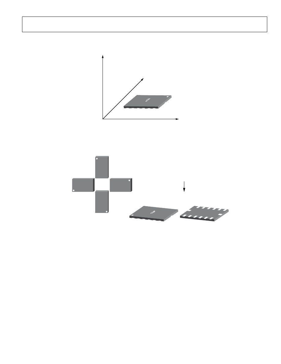
ADXL345
Rev. C | Page 35 of 40
AXES OF ACCELERATION SENSITIVITY
A
Z
A
Y
A
X
07
92
5-
0
21
Figure 57. Axes of Acceleration Sensitivity (Corresponding Output Voltage Increases When Accelerated Along the Sensitive Axis)
07
92
5-
02
2
GRAVITY
X
OUT
= 1g
Y
OUT
= 0g
Z
OUT
= 0g
TOP
X
OUT
= –1g
Y
OUT
= 0g
Z
OUT
= 0g
TOP
X
OUT
= 0g
Y
OUT
= 1g
Z
OUT
= 0g
TO
P
X
OUT
= 0g
Y
OUT
= –1g
Z
OUT
= 0g
TO
P
X
OUT
= 0g
Y
OUT
= 0g
Z
OUT
= 1g
X
OUT
= 0g
Y
OUT
= 0g
Z
OUT
= –1g
Figure 58. Output Response vs. Orientation to Gravity
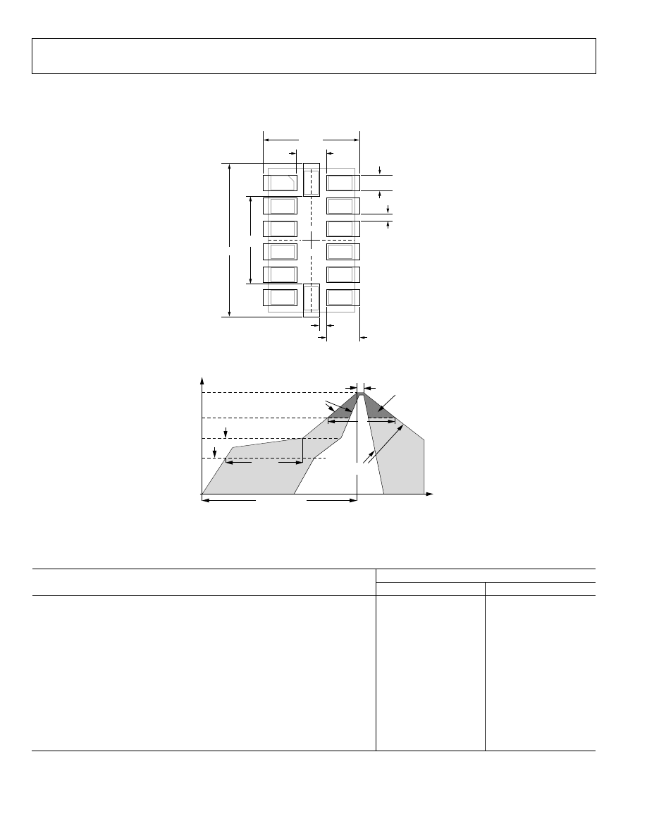
ADXL345
Rev. C | Page 36 of 40
LAYOUT AND DESIGN RECOMMENDATIONS
Figure 59 shows the recommended printed wiring board land pattern. Figure 60
and Table 24 provide details about the recommended
soldering profile.
3.3400
0.5500
0.2500
3.0500
0.2500
1.1450
5.3400
1.0500
0
79
25
-01
4
Figure 59. Recommended Printed Wiring Board Land Pattern (Dimensions shown in millimeters)
t
P
t
L
t
25°C TO PEAK
t
S
PREHEAT
CRITICAL ZONE
T
L
TO T
P
TE
M
P
E
R
A
T
U
R
E
TIME
RAMP-DOWN
RAMP-UP
T
SMIN
T
SMAX
T
P
T
L
0
792
5-
0
15
Figure 60. Recommended Soldering Profile
Table 24. Recommended Soldering Profile
Condition
Profile Feature
Sn63/Pb37
Pb-Free
Average Ramp Rate from Liquid Temperature (T
L
) to Peak Temperature (T
P
)
3°C/sec maximum
3°C/sec maximum
Preheat
Minimum Temperature (T
SMIN
) 100°C
150°C
Maximum Temperature (T
SMAX
) 150°C
200°C
Time from T
SMIN
to T
SMAX
(t
S
)
60 sec to 120 sec
60 sec to 180 sec
T
SMAX
to T
L
Ramp-Up Rate
3°C/sec maximum
3°C/sec maximum
Liquid Temperature (T
L
)
183°C
217°C
Time Maintained Above T
L
(t
L
)
60 sec to 150 sec
60 sec to 150 sec
Peak Temperature (T
P
)
240 + 0/−5°C
260 + 0/−5°C
Time of Actual T
P
− 5°C (t
P
)
10 sec to 30 sec
20 sec to 40 sec
Ramp-Down Rate
6°C/sec maximum
6°C/sec maximum
Time 25°C to Peak Temperature
6 minutes maximum
8 minutes maximum
1
Based on JEDEC Standard J-STD-020D.1.
2
For best results, the soldering profile should be in accordance with the recommendations of the manufacturer of the solder paste used.
ADXL345
Rev. C | Page 37 of 40
OUTLINE DIMENSIONS
BOTTOM VIEW
TOP VIEW
END VIEW
SEATING
PLANE
1.00
0.95
0.85
5.00
BSC
3.00
BSC
PAD A1
CORNER
0.79
0.74
0.69
1
6
7
8
14
13
0.80
BSC
1.01
1.50
0.49
0.50
0.49
0.813
×
0.50
03-16-
2010-A
Figure 61. 14-Terminal Land Grid Array [LGA]
(CC-14-1)
Solder Terminations Finish Is Au over Ni
Dimensions shown in millimeters
ORDERING GUIDE
Measurement
Range (g)
Specified
Voltage (V)
Temperature Range
Package Description
Package
Option
ADXL345BCCZ
±2, ±4, ±8, ±16
2.5
−40°C to +85°C
14-Terminal Land Grid Array [LGA]
CC-14-1
ADXL345BCCZ-RL
±2, ±4, ±8, ±16
2.5
−40°C to +85°C
14-Terminal Land Grid Array [LGA]
CC-14-1
ADXL345BCCZ-RL7
±2, ±4, ±8, ±16
2.5
−40°C to +85°C
14-Terminal Land Grid Array [LGA]
CC-14-1
EVAL-ADXL345Z
Evaluation
Board
EVAL-ADXL345Z-DB
Evaluation
Board
EVAL-ADXL345Z-M
Analog Devices Inertial Sensor Evaluation
System, Includes ADXL345 Satellite
EVAL-ADXL345Z-S
ADXL345 Satellite, Standalone
1
Z = RoHS Compliant Part.

ADXL345
Rev. C | Page 38 of 40
NOTES

ADXL345
Rev. C | Page 39 of 40
NOTES

ADXL345
Rev. C | Page 40 of 40
NOTES
I
2
C refers to a communications protocol originally developed by Philips Semiconductors (now NXP Semiconductors).
Analog Devices offers specific products designated for automotive applications; please consult your local Analog Devices sales representative for details. Standard products sold by
Analog Devices are not designed, intended, or approved for use in life support, implantable medical devices, transportation, nuclear, safety, or other equipment where malfunction
of the product can reasonably be expected to result in personal injury, death, severe property damage, or severe environmental harm. Buyer uses or sells standard products for use
in the above critical applications at Buyer's own risk and Buyer agrees to defend, indemnify, and hold harmless Analog Devices from any and all damages, claims, suits, or expenses
resulting from such unintended use.
©2009–2011 Analog Devices, Inc. All rights reserved. Trademarks and
registered trademarks are the property of their respective owners.
D07925-0-5/11(C)
Document Outline
- FEATURES
- APPLICATIONS
- GENERAL DESCRIPTION
- FUNCTIONAL BLOCK DIAGRAM
- TABLE OF CONTENTS
- REVISION HISTORY
- SPECIFICATIONS
- ABSOLUTE MAXIMUM RATINGS
- PIN CONFIGURATION AND FUNCTION DESCRIPTIONS
- TYPICAL PERFORMANCE CHARACTERISTICS
- THEORY OF OPERATION
- SERIAL COMMUNICATIONS
- REGISTER MAP
- REGISTER DEFINITIONS
- Register 0x00—DEVID (Read Only)
- Register 0x1D—THRESH_TAP (Read/Write)
- Register 0x1E, Register 0x1F, Register 0x20—OFSX, OFSY, OFSZ (Read/Write)
- Register 0x21—DUR (Read/Write)
- Register 0x22—Latent (Read/Write)
- Register 0x23—Window (Read/Write)
- Register 0x24—THRESH_ACT (Read/Write)
- Register 0x25—THRESH_INACT (Read/Write)
- Register 0x26—TIME_INACT (Read/Write)
- Register 0x27—ACT_INACT_CTL (Read/Write)
- Register 0x28—THRESH_FF (Read/Write)
- Register 0x29—TIME_FF (Read/Write)
- Register 0x2A—TAP_AXES (Read/Write)
- Register 0x2B—ACT_TAP_STATUS (Read Only)
- Register 0x2C—BW_RATE (Read/Write)
- Register 0x2D—POWER_CTL (Read/Write)
- Register 0x2E—INT_ENABLE (Read/Write)
- Register 0x2F—INT_MAP (R/)
- Register 0x30—INT_SOURCE (Read Only)
- Register 0x31—DATA_FORMAT (Read/Write)
- Register 0x32 to Register 0x37—DATAX0, DATAX1, DATAY0, DATAY1, DATAZ0, DATAZ1 (Read Only)
- Register 0x38—FIFO_CTL (Read/Write)
- 0x39—FIFO_STATUS (Read Only)
- REGISTER DEFINITIONS
- APPLICATIONS INFORMATION
- POWER SUPPLY DECOUPLING
- MECHANICAL CONSIDERATIONS FOR MOUNTING
- TAP DETECTION
- THRESHOLD
- LINK MODE
- SLEEP MODE VS. LOW POWER MODE
- OFFSET CALIBRATION
- USING SELF-TEST
- DATA FORMATTING OF UPPER DATA RATES
- NOISE PERFORMANCE
- OPERATION AT VOLTAGES OTHER THAN 2.5 V
- OFFSET PERFORMANCE AT LOWEST DATA RATES
- AXES OF ACCELERATION SENSITIVITY
- LAYOUT AND DESIGN RECOMMENDATIONS
- OUTLINE DIMENSIONS
Wyszukiwarka
Podobne podstrony:
3axis Digital Accelerometer ST AIS326DQ id 36590
DIGITAL OUTPUT ANGULAR ACCELEROMETER 8556
DIGITAL OUTPUT ANGULAR ACCELEROMETER 8556
Principles of Sigma Delta Conversion for Analog to Digital Converters
Page153 Model 2491 2492 2493 Digital Switchboard meter c
Digital ECU Tuner III Manual
przekaz digitalny
Ebook Spraw 2 Netpress Digital
(1 1)Fully Digital, Vector Controlled Pwm Vsi Fed Ac Drives With An Inverter Dead Time Compensation
Digital LC Meter Version 2, pcb
Applications of polyphase filters for bandpass sigma delta analog to digital conversion
Plesiochronous Digital Hierarchy
A Digital Control Technique for a single phase PWM inverter
Digital Leveller 2
Kluwer Digital Computer Arithmetic Datapath Design Using Verilog HDL
The Dirty Truth?out The Cloud And The Digital Age
więcej podobnych podstron