
MOTOROLA
APR8
by
Sangil Park, Ph. D.
Strategic Applications
Digital Signal Processor Operation
Motorola
Digital Signal
Processors
Principles of Sigma-Delta
Modulation for Analog-to-
Digital Converters

Motorola reserves the right to make changes without further notice to any products here-
in. Motorola makes no warranty, representation or guarantee regarding the suitability of
its products for any particular purpose, nor does Motorola assume any liability arising out
of the application or use of any product or circuit, and specifically disclaims any and all
liability, including without limitation consequential or incidental damages. “Typical” pa-
rameters can and do vary in different applications. All operating parameters, including
“Typicals” must be validated for each customer application by customer’s technical ex-
perts. Motorola does not convey any license under its patent rights nor the rights of oth-
ers. Motorola products are not designed, intended, or authorized for use as components
in systems intended for surgical implant into the body, or other applications intended to
support or sustain life, or for any other application in which the failure of the Motorola
product could create a situation where personal injury or death may occur. Should Buyer
purchase or use Motorola products for any such unintended or unauthorized application,
Buyer shall indemnify and hold Motorola and its officers, employees, subsidiaries, affili-
ates, and distributors harmless against all claims, costs, damages, and expenses, and
reasonable attorney fees arising out of, directly or indirectly, any claim of personal injury
or death associated with such unintended or unauthorized use, even if such claim alleges
that Motorola was negligent regarding the design or manufacture of the part. Motorola
and
are registered trademarks of Motorola, Inc. Motorola, Inc. is an Equal Opportuni-
ty/Affirmative Action Employer.

Table
of Contents
MOTOROLA
iii
I
ntroduction
Conventional Analog-to-Digital Converters
Quantization Error in A/D Conversion
Oversampling and Decimation Basics
Delta Modulation
Sigma-Delta modulation for A/D Converters
(Noise Shaping)
6.1
Analysis of Sigma-Delta Modulation in
Z-Transform Domain
Digital Decimation Filtering
7.1
Comb-Filter Design as a Decimator
7.2
Second Section Decimation FIR Filter
Mode Resolution by Filtering the Comb-Filter
Out
put with Half-Band Filters
Summary
SECTION 1
SECTION 2
SECTION 3
SECTION 4
SECTION 5
SECTION 6
SECTION 7
SECTION 8
SECTION 9
REFERENCES
1-1
2-1
3-1
4-1
5-1
6-1
6-6
7-1
7-5
7-10
8-1
9-1
References-1

MOTOROLA
v
Illustrations
Generalized Analog-to-Digital Conversion Process
Conventional Analog-to-Digital Conversion Process
Spectra of Analog and Sampled Signals
Quantization Error
Noise Spectrum of Nyquist Samplers
Comparison Between Nyquist Samplers and 2X
Oversamplers
Anti-Aliasing Filter Response and Noise Spectrum of
Oversampling A/D Converters
Frequency Response of Analog Anti-Aliasing Filters
Simple Example of Decimation Process
Delta Modulation and Demodulation
Derivation of Sigma-Delta Modulation from
Delta Modulation
Block Diagram of Sigma-Delta Modulation
S-Domain Analysis of Sigma-Delta Modulator
Block Diagram of First-Order Sigma-Delta A/D
Converter
Input and Output of a First-Order Sigma-Delta
Modulator
Z-Domain Analysis of First-Order Noise Shaper
Spectrum of a First-Order Sigma-Delta
Noise Shaper
2-2
2-3
2-5
3-3
3-3
4-3
4-5
4-6
4-7
5-2
6-1
6-2
6-3
6-5
6-6
6-7
6-9
Figure 2-1
Figure 2-2
Figure 2-3
Figure 3-1
Figure 3-2
Figure 4-1
Figure 4-2
Figure 4-3
Figure 4-4
Figure 5-1
Figure 6-1
Figure 6-2
Figure 6-3
Figure 6-4
Figure 6-5
Figure 6-6
Figure 6-7

vi
MOTOROLA
Illustrations
Second-Order and Third-Order Sigma-Delta
Noise Shapers
Multi-Order Sigma-Delta Noise Shapers
Spectra of Three Sigma-Delta Noise Shapers
Digital Decimation Process
Block Diagram of One-Stage Comb Filtering
Process
Transfer Function of a Comb-Filter
Cascaded Structure of a Comb-Filter
Aliased Noise in Comb-Filter Output
(a) Comb-Filter Magnitude Response in
Baseband
(b) Compensation FIR Filter Magnitude
Response
FIR Filter Magnitude Response
Aliased Noise Bands of FIR Filter Output
Spectrum of a Third-Order Noise Shaper
(16384 FFT bins)
Spectrum of Typical Comb-Filter Output
(4096 FFT bins)
Decimation Process using a Series of
Half Band Filters
Figure 6-8
Figure 6-9
Figure 6-10
Figure 7-1
Figure 7-2
Figure 7-3
Figure 7-4
Figure 7-5
Figure 7-6
Figure 7-7
Figure 7-8
Figure 8-1
Figure 8-2
Figure 8-3
6-10
6-13
6-13
7-4
7-6
7-7
7-8
7-9
7-11
7-11
7-12
7-13
8-2
8-3
8-5

MOTOROLA
vii
Tables
Table 8-1
Parameters for Designing Half-Band Filters
8-4

MOTOROLA
1-1
“Since the
Σ−∆
A/D converters
are based on
digital filtering
techniques,
almost 90% of
the die is
implemented in
digital circuitry
which enhances
the prospect of
compatibility.”
SECTION 1
T
he performance of digital signal processing and
communication systems is generally limited by the
precision of the digital input signal which is achieved
at the interface between analog and digital informa-
tion. Sigma-Delta (
Σ−∆
) modulation based analog-to-
digital (A/D) conversion technology is a cost effective
alternative for high resolution (greater than 12 bits)
converters which can be ultimately integrated on dig-
ital signal processor ICs.
Although the sigma-delta modulator was first intro-
duced in 1962 [1], it did not gain importance until
recent developments in digital VLSI technologies
which provide the practical means to implement the
large digital signal processing circuitry. The increas-
ing use of digital techniques in communication and
audio application has also contributed to the recent in-
terest in cost effective high precision A/D converters.
A requirement of analog-to-digital (A/D) interfaces is
compatibility with VLSI technology, in order to provide
for monolithic integration of both the analog and digi-
tal sections on a single die. Since the
Σ−∆
A/D
converters are based on digital filtering techniques,
almost 90% of the die is implemented in digital circuit-
ry which enhances the prospect of compatibility.
Introduction

1-2
MOTOROLA
Additional advantages of such an approach in-
clude higher reliability, increased functionality, and
reduced chip cost. Those characteristics are com-
monly required in the digital signal processing
environment of today. Consequently, the develop-
ment of digital signal processing technology in
general has been an important force in the devel-
opment of high precision A/D converters which can
be integrated on the same die as the digital signal
processor itself. The objective of this application
report is to explain the
Σ−∆
technology which is im-
plemented in the DSP56ADC16, and show the
superior performance of the converter compared
to the performance of more conventional imple-
mentations. Particularly, this application note
discusses a third-order, noise-shaping oversam-
pling structure.
Conventional high-resolution A/D converters, such
as successive approximation and flash type con-
verters, operating at the Nyquist rate (sampling
frequency approximately equal to twice the maxi-
mum frequency in the input signal), often do not
make use of exceptionally high speeds achieved
with a scaled VLSI technology. These Nyquist sam-
plers require a complicated analog lowpass filter
(often called an anti-aliasing filter) to limit the maxi-
mum frequency input to the A/D, and sample-and-
hold circuitry. On the other hand,
Σ−∆
A/D convert-
ers use a low resolution A/D converter (1-bit
quantizer), noise shaping, and a very high oversam-
pling rate (64 times for the DSP56ADC16). The high
resolution can be achieved by the decimation (sam-
ple-rate reduction) process. Moreover, since

MOTOROLA
1-3
precise component matching or laser trimming is
not needed for the high-resolution
Σ−∆
A/D convert-
ers, they are very attractive for the implementation
of complex monolithic systems that must incorpo-
rate both digital and analog functions. These
features are somewhat opposite from the require-
ments of conventional converter architectures,
which generally require a number of high precision
devices. This application note describes the con-
cepts of noise shaping, oversampling, and
decimation in some detail.
■


MOTOROLA
2-1
“Most A/D
converters can
be classified into
two groups
according to the
sampling rate
criteria: Nyquist
rate
converters...
and
oversampling
converters...”
Conventional
Analog-to-Digital
Converters
SECTION 2
S
ignals, in general, can be divided into two catego-
ries; an analog signal, x(t), which can be defined in a
continuous-time domain and a digital signal, x(n),
which can be represented as a sequence of numbers
in a discrete-time domain as shown in Figure 2-1. The
time index n of a discrete-time signal x(n) is an integer
number defined by sampling interval T. Thus, a dis-
crete-time signal, x*(t), can be represented by a
sampled continuous-time signal x(t) as:
Eqn. 2-1
where:
A practical A/D converter transforms x(t) into a dis-
crete-time digital signal, x*(t), where each sample is
expressed with finite precision. Each sample is ap-
proximated by a digital code, i.e., x(t) is transformed
x
∗
t
( )
x t
( )
δ
t
nT
–
(
)
n
∞
–
=
∞
∑
=
δ
(t) = 1, t = 0
,
0, elsewhere
2-2
MOTOROLA
into a sequence of finite precision or quantized
samples x(n). This quantization process introduc-
es errors which are discussed in
SECTION 3
Quantization Error in A/D Converters
.
Most A/D converters can be classified into two
groups according to the sampling rate criteria.
Nyquist rate converters, such as a successive ap-
proximation register (SAR), double integration,
and oversampling converters, sample analog sig-
nals which have maximum frequencies slightly
less than the Nyquist frequency, f
N
= f
s
/ 2, where
fs is the sampling frequency [2]. Meanwhile, over-
sampling converters perform the sampling
process at a much higher rate, f
N
<< F
s
(e.g., 64
times for the DSP56ADC16), where F
s
denotes
the input sampling rate.
Analog Signal
sample rate f
s
=
Sampling
Quantization
Digital Signal
creates quantization error noise
1
T
---
x (t)
x* (t)
x (n)
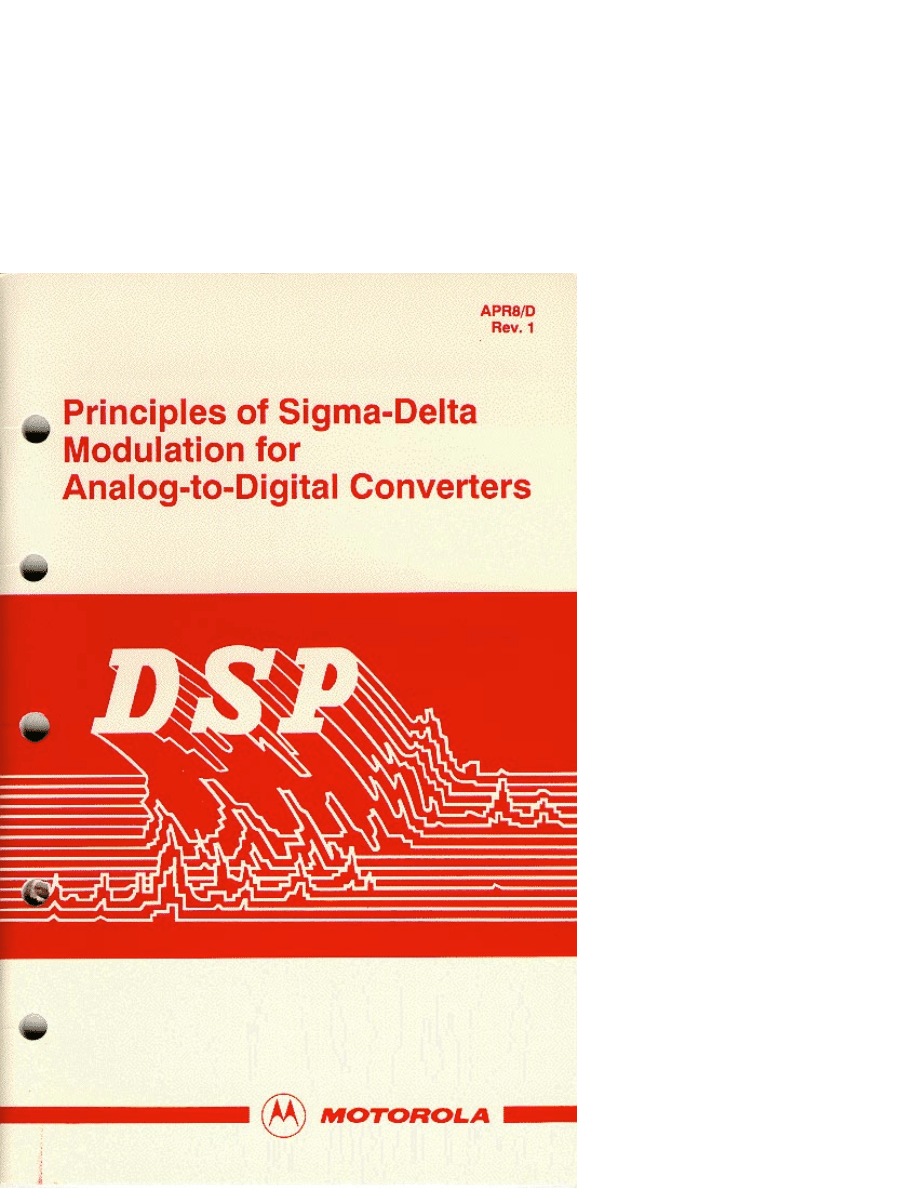
Figure 2-1 Generalized Analog-to-Digital Conversion Process
MOTOROLA
2-3
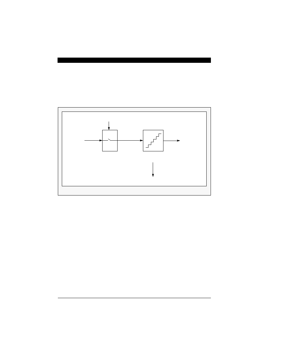
Figure 2-2 illustrates the conventional A/D con-
version process that transforms an analog input
signal x(t) into a sequence of digital codes x(n) at
a sampling rate of f
s
= 1/T, where T denotes the
sampling interval. Since
a periodic function with period T, it can be repre-
sented by a Fourier series given by [5]:
Eqn. 2-2
Combining Eqn. 2-1 and Eqn. 2-2, we get:
Eqn. 2-3
Multi-level
Quantizer
Analog
Signal
Digital
Signal
x (t)
x (n)
001
010
001
000
111
110
101
x (n)
x (t)
Band-limiting
Successive Approximation
Flash Conversion
Dual Slope Method
e.g.:
Figure 2-2 Conventional Analog-to-Digital Conversion Process
Sample and Hold
Circuit
Anti-Aliasing
Filter
δ
t
nT
–
(
)
x t
( )
δ
t
nT
–
(
)
n
∞
–
=
∞
∑
1
T
---
x t
( )
e
j2n
π
t
(
)
T
⁄
n
∞
–
=
∞
∑
=
x
∗
t
( )
1
T
---
x t
( )
e
j2n
π
t
(
)
T
⁄
n
∞
–
=
∞
∑
1
T
---
x t
( )
e
j2
π
f
s
nt
n
∞
–
=
∞
∑
=
=

2-4
MOTOROLA
Eqn. 2-2 states that the act of sampling (i.e., the
sampling function):
is equivalent to modulating the input signal by carri-
er signals having frequencies at 0, f
s
, 2f
s
,. . .. In
other words, the sampled signal can be expressed
in the frequency domain as the summation of the
original signal component and signals frequency
modulated by integer multiples of the sampling fre-
quency as shown in Figure 2-3. Thus, input signals
above the Nyquist frequency, fn, cannot be properly
converted and they also create new signals in the
base-band, which were not present in the original
signal. This non-linear phenomenon is a signal dis-
tortion frequently referred to as aliasing [2]. The
distortion can only be prevented by properly low-
pass filtering the input signal up to the Nyquist
frequency. This lowpass filter, sometimes called the
anti-aliasing filter, must have flat response over the
frequency band of interest (baseband) and attenu-
ate the frequencies above the Nyquist frequency
enough to put them under the noise floor. Also, the
non-linear phase distortion caused by the anti-alias-
ing filter may create harmonic distortion and audible
degradation. Since the analog anti-aliasing filter is
the limiting factor in controlling the bandwidth and
phase distortion of the input signal, a high perfor-
mance anti-aliasing filter is required to obtain high
resolution and minimum distortion.
x t
( )
δ
t
nT
–
(
)
n
∞
–
=
∞
∑
MOTOROLA
2-5
| X (f) |
f
N
f
(a) Frequency response of unlimited signal
f
N
f
f
s
2f
s
3f
s
4f
s
(b) Frequency response of sampled unlimited signal
| X *(f) |
| X (f) |
| X *(f) |
aliased signal
f
N
signal
(c) Frequency response of band-limited analog signal
(d) Frequency response of sampled digital signal
Anti-Aliasing Filter (Band-Limiting)
f
f
f
N
f
s
2f
s
3f
s
4f
s
Figure 2-3 Spectra of Analog and Sampled Signals

2-6
MOTOROLA
In addition to an anti-aliasing filter, a sample-and-
hold circuit is required. Although the analog signal
is continuously changing, the output of the sample-
and-hold circuitry must be constant between sam-
ples so the signal can be quantized properly. This
allows the converter enough time to compare the
sampled analog signal to a set of reference levels
that are usually generated internally [3]. If the out-
put of the sample-and-hold circuit varies during T, it
can limit the performance of the A/D converter
subsystem.
Each of these reference levels is assigned a digital
code. Based on the results of the comparison, a dig-
ital encoder generates the code of the level the
input signal is closest to. The resolution of such a
converter is determined by the number and spacing
of the reference levels that are predefined. For
high-resolution Nyquist samplers, establishing the
reference voltages is a serious challenge.
For example, a 16-bit A/D converter, which is the
standard for high accuracy A/D converters, requires
216 - 1 = 65535 different reference levels. If the
converter has a 2V input dynamic range, the spac-
ing of these levels is only 30 mV apart. This is
beyond the limit of component matching tolerances
of VLSI technologies [4]. New techniques, such as
laser trimming or self-calibration can be employed
to boost the resolution of a Nyquist rate converter
beyond normal component tolerances. However,
these approaches result in additional fabrication
complexity, increased circuit area, and higher cost.
■

MOTOROLA
3-1
T
he process of converting an analog signal (which
has infinite resolution by definition) into a finite range
number system (quantization) introduces an error sig-
nal that depends on how the signal is being
approximated. This quantization error is on the order
of one least-significant-bit (LSB) in amplitude, and it is
quite small compared to full-amplitude signals. How-
ever, as the input signal gets smaller, the quantization
error becomes a larger portion of the total signal.
When the input signal is sampled to obtain the se-
quence x(n), each value is encoded using finite word-
lengths of B-bits including the sign bit. Assuming the
sequence is scaled such that
for fraction-
al number representation, the pertinent dynamic
range is 2. Since the encoder employs B-bits, the
number of levels available for quantizing x(n) is
.
The interval between successive levels, q, is there-
fore given by:
Eqn. 3-1
which is called the quantization step size. The sam-
pled input value
is then rounded to the nearest
level, as illustrated in Figure 3-1.
x n
( )
1
≤
2
B
q
1
2
B 1
–
--------------
=
x
∗
t
( )
Quantization Error in
A/D Conversion
SECTION 3
“For an input
signal which is
large compared
to an LSB step,
the error term
e(n) is a random
quantity in the
interval (-q/2,
q/2) with equal
probability.”

3-2
MOTOROLA
From Eqn. 3-2, it follows that the A/D converter out-
put is the sum of the actual sampled signal
and an error (quantization noise) component e(n);
that is:
Eqn. 3-2
For an input signal which is large compared to an
LSB step, the error term e(n) is a random quantity
in the interval (-q/2, q/2) with equal probability. Then
the noise power (variance),
, can be found as
[5]:
Eqn. 3-3
where:
E denotes statistical expectation
We shall refer to
in Eqn. 3-3 as being the steady-
state input quantization noise power. Figure 3-2
shows the spectrum of the quantization noise. Since
the noise power is spread over the entire frequency
range equally, the level of the noise power spectral
density can be expressed as:
Eqn. 3-4
The concepts discussed in this section apply in
general to A/D converters.
■
x
∗
t
( )
x n
( )
x
∗
t
( )
e n
( )
+
=
σ
e
2
σ
e
2
E e
2
[ ]
1
q
---
e
2
de
q
–
(
)
2
⁄
q 2
⁄
∫
q
2
12
------
2
2B
–
3
------------
=
=
=
=
σ
e
2
N f
( )
q
2
12f
s
-----------
2
2B
–
3f
s
-----------
=
=
MOTOROLA
3-3
..
..
..
..
..
..
..
..
Analog Levels
Digital Words
0001
0000
1111
0.125
0.000
-0.125
q
Figure 3-1 Quantization Error
Figure 3-2 Noise Spectrum of Nyquist Samplers
N f
( )
q
2
12
------
=
1
f
s
----
N (f)
-f
N
f
N
f
S
= 2f
N
Noise Level:


MOTOROLA
4-1
SECTION 4
T
he quantization process in a Nyquist-rate A/D con-
verter is generally different from that in an
oversampling converter. While a Nyquist-rate A/D
converter performs the quantization in a single sam-
pling interval to the full precision of the converter, an
oversampling converter generally uses a sequence of
coarsely quantized data at the input oversampling rate
of
followed by a digital-domain decimation
process to compute a more precise estimate for the
analog input at the lower output sampling rate, f
s
,
which is the same as used by the Nyquist samplers.
Regardless of the quantization process oversampling
has immediate benefits for the anti-aliasing filter. To il-
lustrate this point, consider a typical digital audio
application using a Nyquist sampler and then using a
two times oversampling approach. Note that in the fol-
lowing discussion the full precision of a Nyquist
sampler is assumed. Coarse quantizers will be con-
sidered separately.
The data samples from Nyquist-rate converters are
taken at a rate of at least twice the highest signal fre-
quency of interest. For example, a 48 kHz sampling
rate allows signals up to 24 kHz to pass without
F
s
Nf
s
=
Oversampling and
Decimation Basics
“The benefit of
oversampling is
more than an
economical anti-
aliasing filter.
The decimation
process can be
used to provide
increased
resolution.”

4-2
MOTOROLA
aliasing, but because of practical circuit limitation,
the highest frequency that passes is actually about
22 kHz. Also, the anti-aliasing filter in Nyquist A/D
converters requires a flat response with no phase
distortion over the frequency band of interest (e.g.,
20 kHz in digital audio applications). To prevent sig-
nal distortion due to aliasing, all signals above 24
kHz for a 48 kHz sampling rate must be attenuated
by at least 96 dB for 16 bits of dynamic resolution.
These requirements are tough to meet with an an-
alog low-pass filter. Figure 4-1(a) shows the
required analog anti-aliasing filter response, while
Figure 4-1(b) shows the digital domain frequency
spectrum of the signal being sampled at 48 kHz.
Now consider the same audio signal sampled at
2f
s
, 96 kHz. The anti-aliasing filter only needs to
eliminate signals above 74 kHz, while the filter has
flat response up to 22 kHz. This is a much easier fil-
ter to build because the transition band can be 52 kHz
(22k to 74 kHz) to reach the -96 dB point. However,
since the final sampling rate is 48 kHz, a sample
rate reduction filter, commonly called a decimation
filter, is required but it is implemented in the digital
domain, as opposed to anti-aliasing filters which
are implemented with analog circuitry. Figure 4-1(d)
and Figure 4-1(e) illustrate the analog anti-aliasing
filter requirement and the digital-domain frequency
response, respectively. The spectrum of a required
digital decimation filter is shown in Figure 4-1(f). De-
tails of the decimation process are discussed in
SECTION 7 Digital Decimation Filtering.
MOTOROLA
4-3
f
(a) Anti-aliasing filter response for Nyquist samplers
f
(b) Spectrum of sampled data when f
s
= 48 kHz
(c) Spectrum of sampled data when f
s
= 96 kHz
(d) Anti-aliasing filter response for 2x over-samplers
f
f
22 k
22 k
...
...
.
f
(f) Digital filter response for 2:1 decimation process
24 k
22 k
f
(e) Spectrum of 2x oversampled data when f
s
= 96 kHz
24 k
48 k
72 k
96 k
22 k
192 k
24 k
48 k
72 k
96 k
24 k
48 k
72 k
96 k
24 k
48 k
72 k
96 k
24 k
48 k
72 k
96 k
H f
( )
H* f
( )
H* f
( )
H f
( )
H f
( )
H f
( )
...
...
.
...
...
.
Figure 4-1 Comparison Between Nyquist Samplers and 2X Oversamples

4-4
MOTOROLA
This two-times oversampling structure can be extend-
ed to N times oversampling converters. Figure 4-2(a)
shows the frequency response of a general anti-alias-
ing filter for N times oversamplers, while the spectra
of overall quantization noise level and baseband
noise level after the digital decimation filter is illustrat-
ed in Figure 4-2(b). Since a full precision quantizer
was assumed, the total noise power for oversampling
converters and one times Nyquist samplers are the
same. However, the percentage of this noise that is in
the bandwidth of interest, the baseband noise power
NB is:
Eqn. 4-1
which is much smaller (especially when F
s
is much
larger than f
B
) than the noise power of Nyquist sam-
Figure 4-3 compares the requirements of the anti-
aliasing filter of one times and N times oversampled
Nyquist rate A/D converters. Sampling at the
Nyquist rate mandates the use of an anti-aliasing fil-
ter with very sharp transition in order to provide
adequate aliasing protection without compromising
the signal bandwidth
.
N
B
f
( )
df
f
B
–
f
B
∫
2f
B
F
s
-------
q
2
12
-----
=
=
f
B
MOTOROLA
4-5
F
s
/2
F
s
f
B
Overall Noise Level:
In-Band Noise Level:
Note: One R-C lowpass filter is sufficient for the anti-aliasing filter
N f
( )
q2
12
------
=
1
F
s
------
N
B
N f
( )
df
f
–
B
f
B
∫
q
f
B
2
12
---------
2
F
s
------
=
=
- F
s
/2
F
s
/2
- f
B
f
B
N(f)
anti-aliasing filter’s frequency response
(a)
(b)
Figure 4-2 Anti-Aliasing Filter Response and Noise Spectrum of Oversampling
A/D Converters
4-6
MOTOROLA
The transition band of the anti-aliasing filter of an
oversampled A/D converter, on the other hand, is
much wider than its passband, because anti-aliasing
protection is required only for frequency bands be-
tween
and
, when N = 1, 2, ...,
as shown in Figure 4-2(b). Since the complexity of
the filter is a strong function of the ratio of the width
of the transition band to the width of the passband,
oversampled converters require considerably sim-
pler anti-aliasing filters than Nyquist rate converters
with similar performance. For example, with N = 64,
a simple RC lowpass filter at the converter analog in-
put is often sufficient as illustrated in Figure 4-2(a).
(a) Nyquist rate A/D converters
(b) Oversampling A/D converters
f
F
s
/2 = f
N
F
s
F
s
- f
B
F
s
+ f
B
f
B
f
N
f
s
Figure 4-3 Frequency Response of Analog Anti-Aliasing Filters
NFs
f
B
–
NFs
f
B
+

MOTOROLA
4-7
The benefit of oversampling is more than an eco-
nomical anti-aliasing filter. The decimation process
can be used to provide increased resolution. To see
how this is possible conceptually, refer to Figure 4-4,
which shows an example of 16:1 decimation pro-
cess with 1-bit input samples. Although the input
data resolution is only 1-bit (0 or 1), the averaging
method (decimation) yields more resolution (4 bits
[24 = 16]) through reducing the sampling rate by
16:1. Of course, the price to be paid is high speed
sampling at the input — speed is exchanged for
resolution.
■
Sample Rate Reduction == >> More Resolution
1
0
1
0
0
1
0
1
1
0
0
0
1
0
1
16 1-bit inputs
16 : 1 decimation
average
7
16
------
0.4375
0111
=
=
=================>>
1 multi - bit output
Figure 4-4 Simple Example of Decimation Process


MOTOROLA
5-1
“Delta
modulators,
furthermore,
exhibit slope
overload for
rapidly rising
input signals,
and their
performance is
thus dependent
on the frequency
of the input
signal.”
T
he work on sigma-delta modulation was developed
as an extension to the well established delta modula-
tion [6]. Let’s consider the delta modulation/
demodulation structure for the A/D conversion pro-
cess. Figure 5-1 shows the block diagram of the delta
modulator and demodulator. Delta modulation is
based on quantizing the change in the signal from
sample to sample rather than the absolute value of
the signal at each sample.
Since the output of the integrator in the feedback loop
of Figure 5-1(a) tries to predict the input x(t), the inte-
grator works as a predictor. The prediction error term,
, in the current prediction is quantized
and used to make the next prediction. The quantized
prediction error (delta modulation output) is integrated
in the receiver just as it is in the feed back loop [7].
That is, the receiver predicts the input signals as
The predicted signal is smoothed with a lowpass filter.
Delta modulators, furthermore, exhibit slope overload
for rapidly rising input signals, and their performance
is thus dependent on the frequency of the input signal.
In theory, the spectrum of quantization noise of the
prediction error is flat and the noise level is set by the
1-bit comparator. Note that the signal-to-noise ratio
can be enhanced by decimation processes as shown
x t
( )
x t
( )
–
SECTION 5
Delta Modulation
5-2
MOTOROLA
in Figure 4-2. The Motorola MC3417 Continuously
Variable Slope Delta Modulator operation is based
on delta modulation.
■
1-bit quantizer
Channel
output
1
∫
x(t)-
y(t)
x t
( )
x t
( )
x(t)
x (t)
y(t)
x t
( )
Σ
-
+
Analog
Signal
1
∫
(a) Modulation
(b) Demodulation
x(t)
Lowpass
Filter
Channel
input
y(t)
Analog
Signal
Figure 5-1 Delta Modulation and Demodulation
f
S
T
x(t)
x t
( )
MOTOROLA
6-1
Sigma-Delta
Modulation and
Noise Shaping
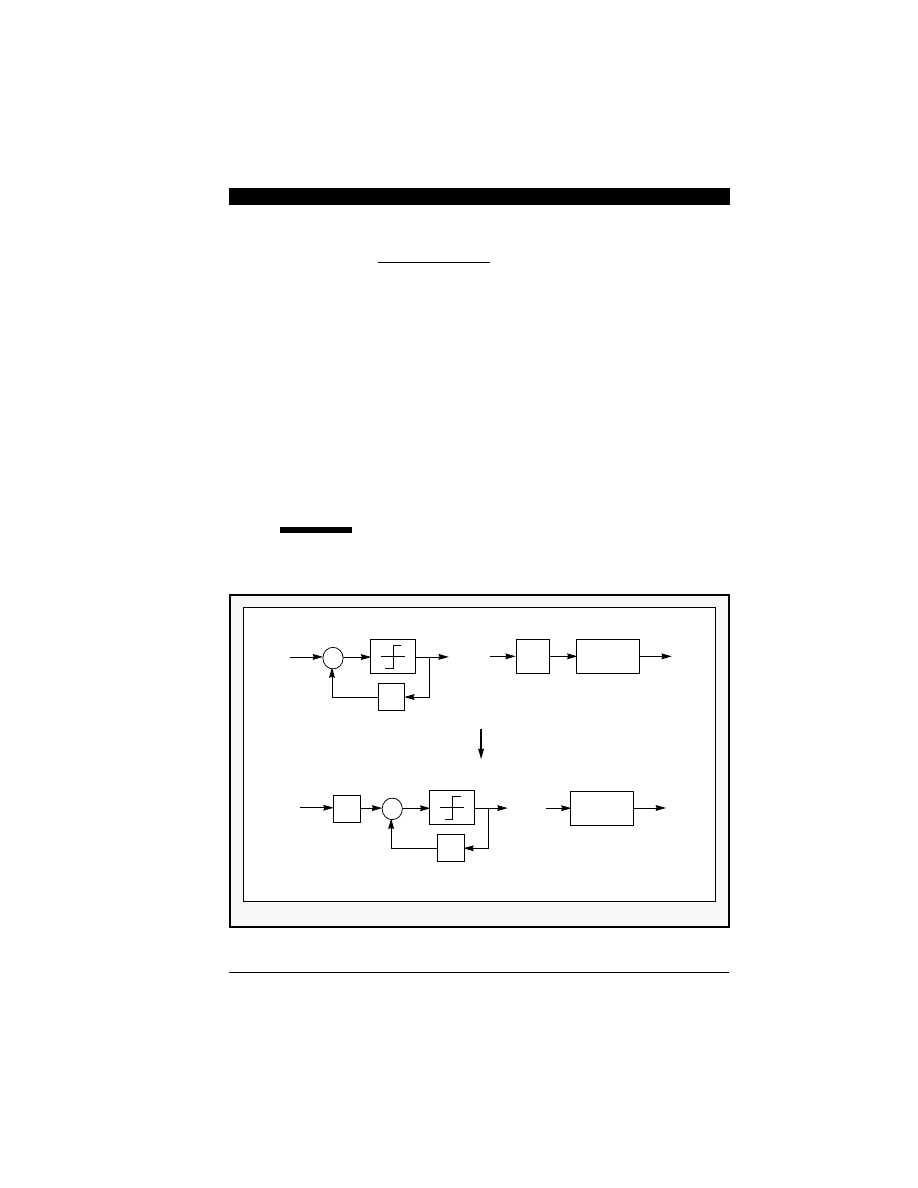
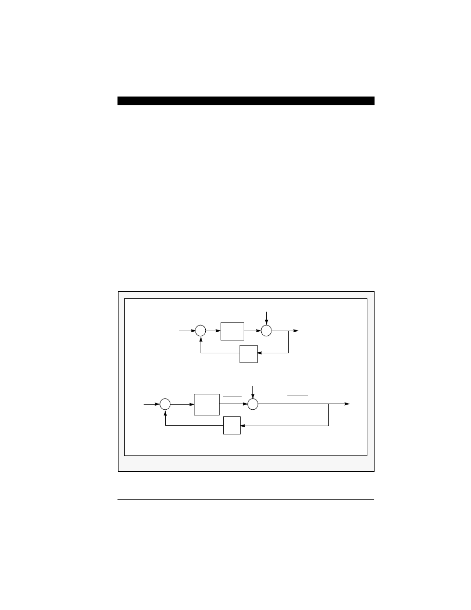
D
elta modulation requires two integrators for modu-
lation and demodulation processes as shown in
Figure 6-1(a). Since integration is a linear operation,
the second integrator can be moved before the mod-
ulator without altering the overall input/output
characteristics. Furthermore, the two integrators in
Figure 6-1 can be combined into a single integrator by
the linear operation property.
1-bit quantizer
Channel
Σ
-
+
Analog
Signal
Modulation
1
∫
1
∫
Lowpass
Filter
Analog
Signal
Demodulation
(a)
Σ
-
+
Analog
Signal
1
∫
1-bit quantizer
1
∫
Channel
Lowpass
Filter
Analog
Signal
(b)
Note: Two Integrators (matched components)
Figure 6-1 Derivation of Sigma-Delta Modulation from Delta Modulation
SECTION 6
“The noise
shaping
property is well
suited to signal
processing...”
6-2
MOTOROLA
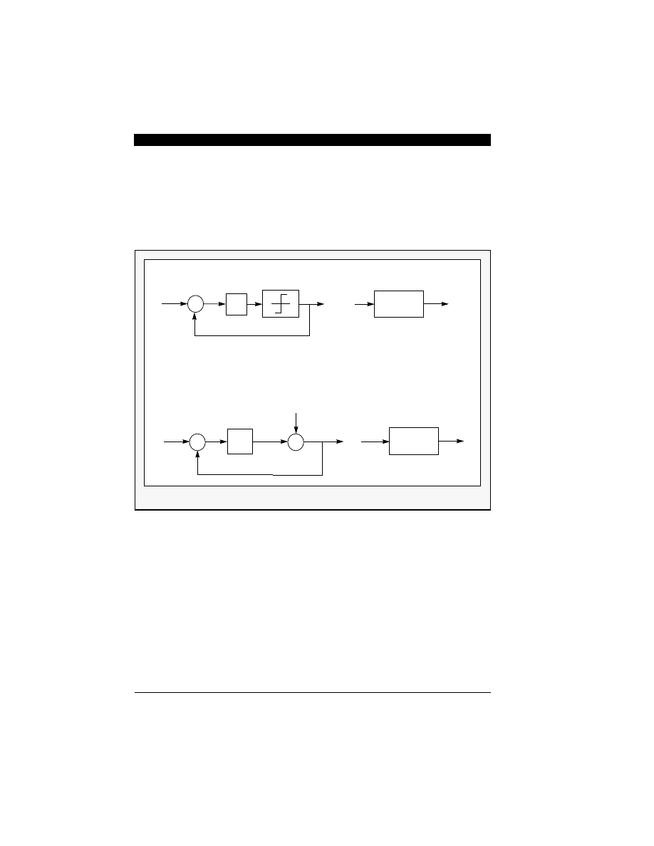
The arrangement shown in Figure 6-2 is called a
Sigma-Delta (
Σ−∆
)
Modulator [1]. This structure,
besides being simpler, can be considered as being
a “
smoothed version” of a 1-bit delta modulator.
The name
Sigma-Delta modulator comes from putting
the integrator (sigma) in front of the delta modulator.
Sometimes, the
Σ−∆
modulator is referred to as an in-
terpolative coder [14]. The quantization noise
characteristic (noise performance) of such a coder is
frequency dependent in contrast to delta modulation.
As will be discussed further, this noise-shaping prop-
erty is well suited to signal processing applications
such as digital audio and communication. Like delta
Integration
Σ
-
+
Modulation
Lowpass
Filter
Demodulation
Σ
-
+
Analog
Signal
1-bit quantizer
1
∫
Channel
Lowpass
Filter
Analog
Signal
Note: Only one integrator
1
S
---
X(s)
Y(s)
Σ
X(s)
+
+
N(s)
Figure 6-2 Block Diagram of Signa-Delta Modulation
MOTOROLA
6-3
modulators, the
Σ−∆
modulators use a simple coarse
quantizer (comparator). However, unlike delta modu-
lators, these systems encode the integral of the signal
itself and thus their performance is insensitive to the
rate of change of the signal.
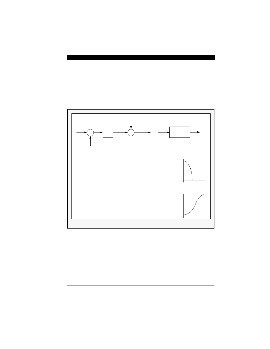
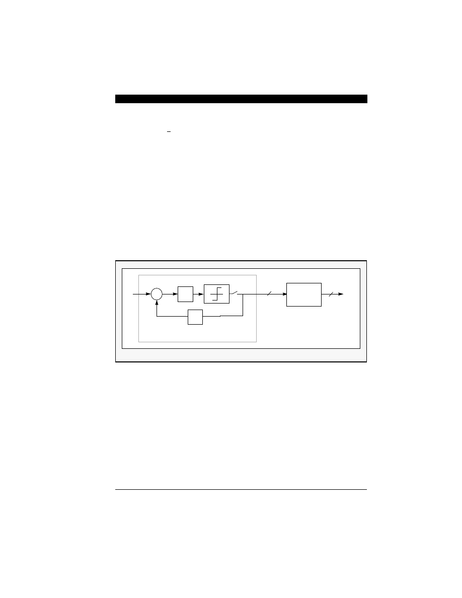
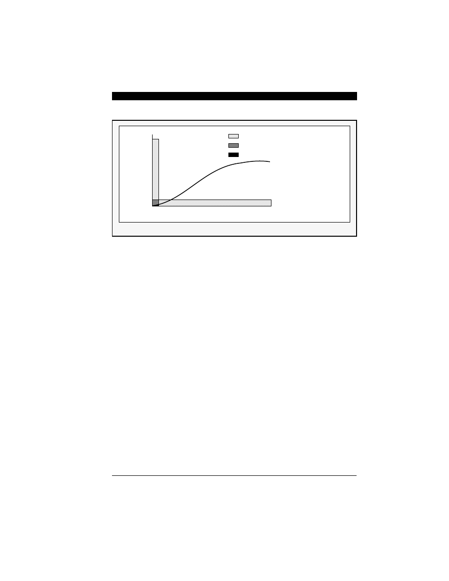
The noise-shaping principle is illustrated by a simpli-
fied
“s-domain” model of a first-order
Σ−∆
modulator
shown in Figure 6-3. The summing node to the right
of the integrator represents a comparator. It’s here
that sampling occurs and quantization noise is add-
ed into the model. The signal-to-noise (S/N)
integration
Σ
-
+
Lowpass
Filter
1
s
---
X(s)
Y(s)
Σ
X(s)
+
+
N(s) : quantization noise
Signal Transfer Function:
(when N(s) = 0)
Noise Transfer Function:
(when X(s) = 0)
Y(s) = [X(s) - Y(s)]
1
s
--
Y s
( )
X s
( )
-----------
1
s
--
1
1
s
--
+
------------
1
s
1
+
------------
=
=
: lowpass filter
Y s
( )
Y s
( )
1
s
--
–
N s
( )
+
=
Y s
( )
N s
( )
-----------
1
1
1
s
--
+
------------
s
s
1
+
------------
=
=
: highpass filter
Figure 6-3 S-Domain Analysis of Sigma-Delta Modulator

6-4
MOTOROLA
transfer function shown in Figure 6-3 illustrates the
modulator’s main action. As the loop integrates the
error between the sampled signal and the input sig-
nal, it lowpass-filters the signal and highpass filters
the noise. In other words, the signal is left unchanged
as long as its frequency content doesn’t exceed the
filter’s cutoff frequency, but the
Σ−∆
loop pushes the
noise into a higher frequency band. Grossly over-
sampling the input causes the quantization noise to
spread over a wide bandwidth and the noise density
in the bandwidth of interest (baseband) to significant-
ly decrease.
Figure 6-4 shows the block diagram of a first-order
oversampled
Σ−∆
A/D converter. The 1-bit digital
output from the modulator is supplied to a digital dec-
imation filter which yields a more accurate
representation of the input signal at the output sam-
pling rate of f
s
. The shaded portion of Figure 6-4 is a
first-order
Σ−∆
modulator. It consists of an analog dif-
ference node, an integrator, a 1-bit quantizer (A/D
converter), and a 1-bit D/A converter in a feed back
structure. The modulator output has only 1-bit (two-
levels) of information, i.e., 1 or -1. The modulator out-
put y(n) is converted to
by a 1-bit D/A
The input to the integrator in the modulator is the
difference between the input signal x(t) and the
quantized output value y(n) converted back to the
predicted analog signal, x(t). Provided that the D/A
converter is perfect, and neglecting signal delays,
x t
( )
MOTOROLA
6-5
this difference between the input signal
x(t) and the
fed back signal x(t) at the integrator input is equal to
the quantization error. This error is summed up in
the integrator and then quantized by the 1-bit A/D
converter. Although the quantization error at every
sampling instance is large due to the coarse nature
of the two level quantizer, the action of the
Σ−∆
modulator loop is to generate a
output which
can be averaged over several input sample periods
to produce a very precise result. The averaging is
performed by the decimation filter which follows the
modulator as shown in Figure 6-4.
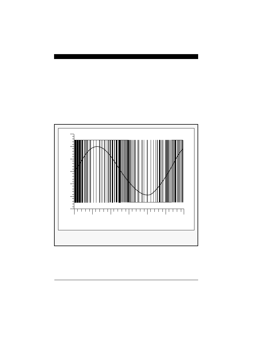
The waveforms of x(t) and y(n) for a first-order
Σ−∆
modulator are illustrated in Figure 6-5 when the in-
put signal is a sinusoid. The modulator performs
both the sampling and the quantization operation in
this example, as is typical for circuit implementa-
tions of
Σ−∆
modulators. In each clock cycle, the
value of the output of the modulator is either plus or
minus full scale, according to the results of the 1-bit
A/D conversion. When the sinusoidal input to the
1
±
Σ
-
+
1
∫
Digital
Decimation
1-bit
D/A
Filter
y(n)
F
s
16
6.4 MHz
(1 bit)
x(t)
y(t)
loop
Σ∆
First order
1
x(n)
100 kHz
(16 bits)
Figure 6-4 Block Diagram of First-Order Sigma-Delta A/D converter
F
s :
f
s
6-6
MOTOROLA
modulator is close to a plus full scale, the output is
positive during most clock cycles. A similar state-
ment holds for the case when the sinusoid is close
to minus full scale. In both cases, the local average
of the modulator output tracks the analog input.
When the input is near zero, the value of the modu-
lator output varies rapidly between a plus and a
minus full scale with approximately zero mean.
Figure 6-5 Input and Output of a First-Order Sigma-Delta Modulator
0.6
0.4
0.2
0.0
-0.2
-0.4
-0.6
0
50
100
150
200
250
300
TIME [t/T]
MOTOROLA
6-7
6.1 Analysis of Sigma-Delta
Modulation in the
Z-Transform Domain
Consider the first-order loop shown in Figure 6-6.
The z-domain transfer function of an integrator is de-
noted by I(z) and the 1-bit quantizer is modeled as
an additive noise source. Standard discrete-time
signal analysis yields:
Eqn. 6-2
Y z
( )
Q z
( )
I z
( )
X z
( )
z
1
–
Y z
( )
–
[
]
+
=
X(z)
Σ
-
+
Σ
Q (Quantization Noise)
z
-1
Y(z)
I(z)
integrator
quantizer
Σ
X(z)
Σ
z
-1
Y(z)
Q
-
+
X - Yz
-1
X - Yz
-1
1 -z
-1
+
+
Y = Q +X - Yz
-1
1 -z
-1
= > X + Q(1 -z
-1
)
integrator
quantizer
1
1
z 1
–
–
----------------
Note: In-band quantization noise is moved out-of-band
Figure 6-6 Z-Domain Analysis of First-Order Noise-Shaper
(a)
(b)
input with
shaped noise

6-8
MOTOROLA
and can be solved for Y(z) as:
Eqn. 6-3
Since an ideal integrator is defined as:
Eqn. 6-4
the first-order
Σ−∆
loop output can be simplified to:
Eqn. 6-5
Since the quantization noise is assumed to be ran-
dom, the differentiator (1-z
-1
doubles the power of quantized noise. However, the
error has been pushed towards high frequencies
due to the differentiator, (1-z
-1
), factor. Therefore,
provided that the analog input signal to the modula-
tor, x(t), is oversampled, the high-frequency
quantization noise can be removed by digital low-
pass filters without affecting the input signal
characteristics residing in baseband. This lowpass
filtering is part of the decimation process.
That is, after the digital decimation filtering pro-
cesses, the output signal has only the frequency
components from 0 Hz to f
B
. Thus, the perfor-
mance of first-order
Σ−∆
modulators can be
compared to the conventional 1-bit Nyquist sam-
plers and the delta-modulation type oversamplers.
Y z
( )
X z
( )
I z
( )
1
I z
( )
z
1
–
+
-------------------------
Q z
( )
1
1
I z
( )
z
1
–
+
-------------------------
+
=
I z
( )
1
1
z
1
–
–
---------------
=
Y z
( )
X z
( )
1
z
1
–
–
(
)
Q z
( )
+
=
MOTOROLA
6-9
Figure 6-7 shows the spectrum of a first-order
Σ−∆
noise-shaper described in Figure 6-6. As shown in
Figure 6-7, the baseband (up to
f
B
) noise of the
Σ−∆
converters appears to be much smaller than Nyquist
samplers or delta modulators. However, for the first
order modulator discussed, the baseband noise
can not reach below the -96 dB signal-to-noise ra-
tio needed for 16-bit A/D converters.
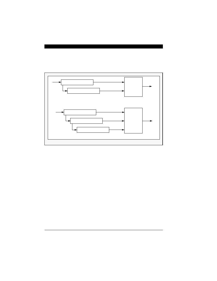
The higher order cascaded (feed-forward)
Σ−∆
mod-
ulators have been introduced and implemented [8-
10]. The block diagrams of second and third order
Σ−∆
modulators are shown in Figure 6-8. Since
these cascaded structures use a noise feed-forward
scheme, the system is always stable and the analy-
sis is simpler compared to the second-order
feedback
Σ−∆
modulators [11-13] and higher order
interpolative coders with feedback loops [14,15].
When multiple first-order
Σ−∆
loops are cascaded to
obtain higher order modulators, the signal that is
passed to the successive loop is the error term from
In-Band noise of Nyquist Samplers
In-Band noise Oversamplers
In-Band noise of Noise-Shaped Oversamplers
First order Sigma-Delta Modulator
Oversampler
Frequency
Power
Density
Nyquist
Sampler (1 bit)
f
B
F
S
/2
Figure 6-7 Spectrum of a First-Order Sigma-Delta Noise Shaper
6-10
MOTOROLA
the current loop. This error is the difference between
the integrator output and the quantization output.
If the input signals to the second and third stage
Σ−∆
loops are Q
1
and Q
2
, respectively, the quanti-
zation output for the second order
Σ−∆
modulator is
given by:
Eqn.
6-6
which yields the second-order
Σ−∆
modulator output
Eqn. 6-7
where:
Y(z) is the z-transform of y(n) which is the
sampled and quantized signal of x(t) at t = n
Figure 6-8 Second-Order and Third-Order Sigma-Delta Noise Shapers
First order Noise Shaper
First order Noise Shaper
(a) Second-Order Noise Shaper
Bit
manipulation
node
First order Noise Shaper
(b) Third-Order Sigma-Delta Noise Shaper
y(n)
y(n)
x(t)
Q1
Q2
y
1
(n)
y
2
(n)
y
1
(n)
y
2
(n)
y
3
(n)
First order Noise Shaper
First order Noise Shaper
x(t)
Q1
Bit
manipulation
node
Y
2
z
( )
Q
1
z
( )
1
z
1
–
–
(
)
Q
2
z
( )
+
=
Y z
( )
X z
( )
1
z
1
–
–
(
)
2
Q
2
z
( )
+
=

MOTOROLA
6-11
Similarly, for the third order
Σ−∆
modulator:
Eqn. 6-8
and, after combining the individual output terms we
obtain:
Eqn. 6-9
where:
Q
3
is the quantization noise from the
third
Σ−∆
loop
Essentially, the noise shaping function in a
Σ−∆
modulator is the inverse of the transfer function of
the filter [1-z
-1
]
-1
in the forward path of the modula-
tor. A filter with higher gain at low frequencies is
expected to provide better baseband attenuation for
the noise signal. Therefore, modulators with more
than one
Σ−∆
loop such as the third-order system
shown in Figure 6-8(b), perform a higher order dif-
ference operation of the error produced by the
quantizer and thus stronger attenuation at low fre-
quencies for the quantization noise signal. The
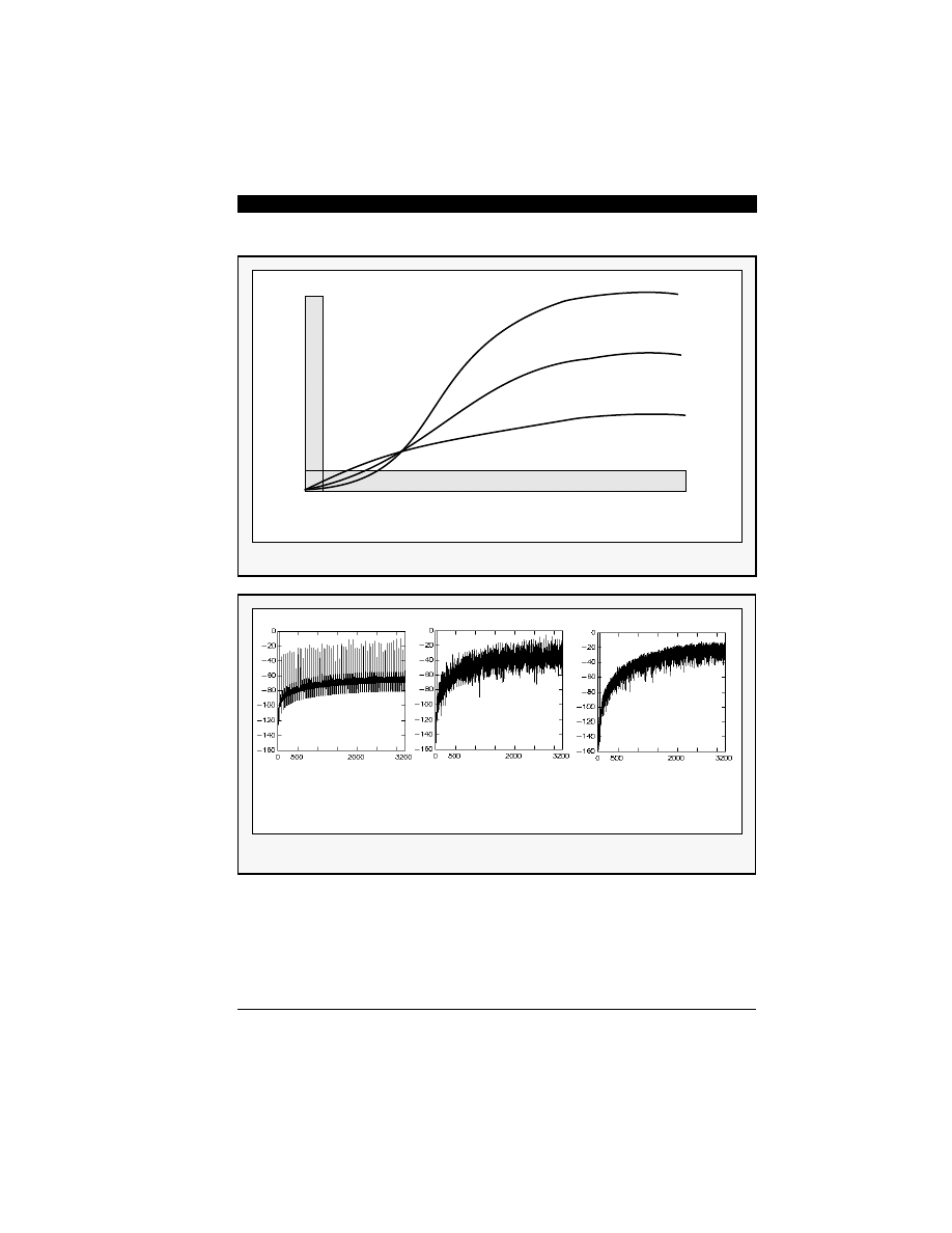
noise shaping functions of second-order and third-
order modulators are compared to that of a first-order
system in Figure 6-9. The baseband quantization er-
ror power for the third-order system is clearly smaller
than for the first-order modulator.
The above analysis can be extended to yield quantita-
tive results for the resolution of
Σ−∆
modulators,
provided that the spectral distribution of the quantiza-
tion error q(n) is known. It has been shown that the
error generated by a scalar quantizer with quantization
Y
3
z
( )
Q
2
z
( )
1
z
1
–
–
(
)
Q
3
z
( )
+
=
Y z
( )
X z
( )
1
z
1
–
–
(
)
3
Q
3
z
( )
+
=

6-12
MOTOROLA
levels equally spaced by q is uncorrelated, assum-
ing that the number of quantization levels is large
and the quantized signal is active [16,17]. This result
is not rigorously applicable to
Σ−∆
modulators, how-
ever, because
Σ−∆
quantizers only have two levels.
Hence, the noise and signal are somewhat correlat-
ed. Nevertheless, analysis based on this
uncorrelated assumption yields correct results in
many cases. Often these analytical results provide a
more intuitive interpretation for the operation of the
modulator than those obtained from computer simu-
lations. The latter, however, will always be
presented to demonstrate the correctness of the an-
alytical result in a particular case.
The performance of this triple cascaded structure
can also be compared by inputting a single sinusoi-
dal signal to the structure and plotting the spectra.
Figure 6-10 shows the frequency response of the
three modulator outputs. The frequency ranges of
the x-axis is up to half of the input sampling frequen-
cy (3.2 MHz for 6.4 MHz input sampling rate). Note
that the frequency of interest is up to 50 kHz which
is a very small portion of the plots.
MOTOROLA
6-13
■
First Order
Σ∆
Modulator
Oversampler
Frequency
Nyquist Sampler (1 bit)
f
B
F
S
/2
Second Order
Σ∆
Modulator
Third Order
Σ∆
Modulator
Figure 6-9 Multi-Order Sigma-Delta Noise Shapers
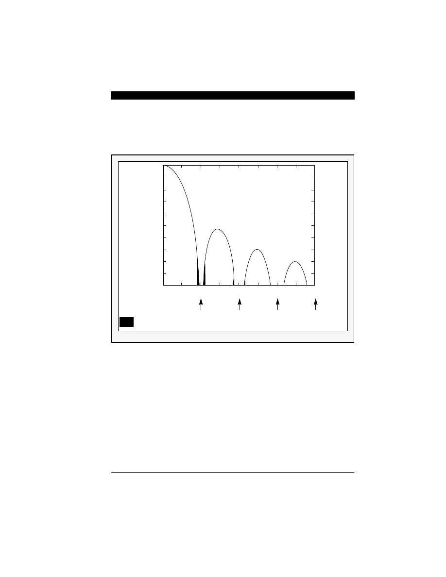
Note: Higher order Noise Shaper has less baseband noise
Figure 6-10 Spectra of Three Sigma-Delta Noise Shapers
(a) First order sigma-delta
(b) Second order sigma-delta
(c) Third order sigma-delta
NOTE: Frequency band of interest (in-band): 0 - 5 kHz
Rest of frequency band will be removed by digital decimation filters


MOTOROLA
7-1
F
iltering noise which could be aliased back into the
baseband is the primary purpose of the digital filter-
ing stage. Its secondary purpose is to take the 1-bit
data stream that has a high sample rate and trans-
form it into a 16-bit data stream at a lower sample
rate. This process is known as decimation. Essen-
tially, decimation is both an averaging filter function
and a rate reduction function performed simulta-
neously.
The output of the modulator is a coarse quantization
of the analog input. However, the modulator is over-
sampled at a rate that is as much as 64 times higher
than the Nyquist rate for the DSP56ADC16. High
resolution is achieved by averaging over 64 data
points to interpolate between the coarse quantiza-
tion levels of the modulator. The process of
averaging is equivalent to lowpass filtering in the fre-
quency domain. With the high frequency
components of the quantization noise removed, the
output sampling rate can be reduced to the Nyquist
rate without aliasing noise into the baseband.
SECTION 7
Digital Decimation
Filtering
“The simplest
and most
economical
filter to reduce
the input
sampling rate is
a ‘Comb-Filter’
because it does
not require a
multiplier.”

7-2
MOTOROLA
Three basic tasks are performed in the digital filter
sections:
1. Remove shaped quantization noise: The
Σ−∆
modulator is designed to suppress quantization
noise in the baseband. Thus, most of the
quantization noise is at frequencies above the
baseband. The main objective of the digital filter
is to remove this out-of-band quantization noise.
This leaves a small amount of baseband
quantization noise and the band-limited input
signal component. Reducing the baseband
quantization noise is equivalent to increasing
the effective resolution of the digital output.
2. Decimation (sample rate reduction): The output
of the
Σ−∆
modulator is at a very high sampling
rate. This is a fundamental characteristic of
Σ−∆
modulators because they use the high
frequency portion of the spectrum to place the
bulk of the quantization noise. After the high
frequency quantization noise is filtered out, it is
possible to reduce the sampling rate. It is
desirable to bring the sampling rate down to the
Nyquist rate which minimizes the amount of
information for subsequent transmission,
storage, or digital signal processing.
3. Anti-aliasing: In practice, the input signals are
seldom completely band-limited. Since the
modulator is sampling at a rate much higher
than the output Nyquist rate, the analog anti-
aliasing filter before the modulator can roll off
gradually. When the digital processor reduces
the sampling rate down to the Nyquist rate, it
needs to provide the necessary additional
aliasing rejection for the input signal as opposed
to the internally generated quantization noise.
There are a number of factors that make it difficult
to implement the digital decimation filter. The input
sampling rate of the modulator is very high and the

MOTOROLA
7-3
digital decimation filter must perform computation-
ally intensive signal processing algorithms in real
time. Furthermore, higher order modulators pro-
duce highly shaped noise as indicated in the
spectrum shown in Figure 6-7 and Figure 6-8.
Thus, the decimation filter must perform very well
to remove the excess quantization noise. Applica-
tions like high quality audio conversion impose the
additional constraint that the digital signal pro-
cessing must perform its task without distorting the
magnitude and phase characteristics of the input
signal in the baseband. The goal is to implement
the digital filter in a minimum amount of logic and
make it feasible for monolithic implementation.
The simplest and most economical filter to reduce
the input sampling rate is a
“Comb-Filter”, because
such a filter does not require a multiplier. A multipli-
er is not required because the filter coefficients are
all unity. This comb-filter operation is equivalent to
a rectangular window finite impulse response (FIR)
filter. However, the comb-filter is not very effective
at removing the large volume of out-of-band quanti-
zation noise generated by the
Σ−∆
modulators and
is seldom used in practice without additional digital
filters. Also, the frequency response of the comb-fil-
ter can cause substantial magnitude drooping at the
upper region of baseband. For many applications
which cannot tolerate this distortion, the comb-filter
must be used in conjunction with one or more addi-
tional digital filter stages.
7-4
MOTOROLA
In the DSP56ADC16 a total of two filter sections
were used as follows [10]:
1. The sampling rate from the
Σ−∆
modulator is
reduced by a factor of 16 with the comb-filter
section as shown in Figure 7-1. A four-stage
comb-filter was used to decimate the third order
modulator on the DSP56ADC16 [17,18].
2. The second section is a FIR lowpass filter with
symmetric coefficient values to maintain a
linear-phase response. It provides 4:1
decimation and magnitude compensation for the
magnitude change (droop) from the comb-filter
output. The FIR filter coefficients are also
computed to equalize the baseband frequency
response to within
dB of a flat
response.
Σ−∆
loops
16:1
Comb Filter
4:1
FIR Filter
6.4 MHz
1-bit Resolution
400 kHz
12-bit Resolution
100 kHz
16-bit Resolution
16
1
16
Digital
Outputs
Analog
Input
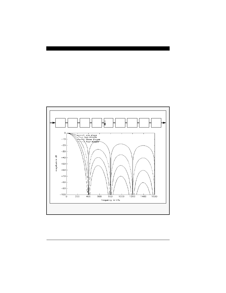
Figure 7-1 Digital Decimation Process
0.001
±

MOTOROLA
7-5
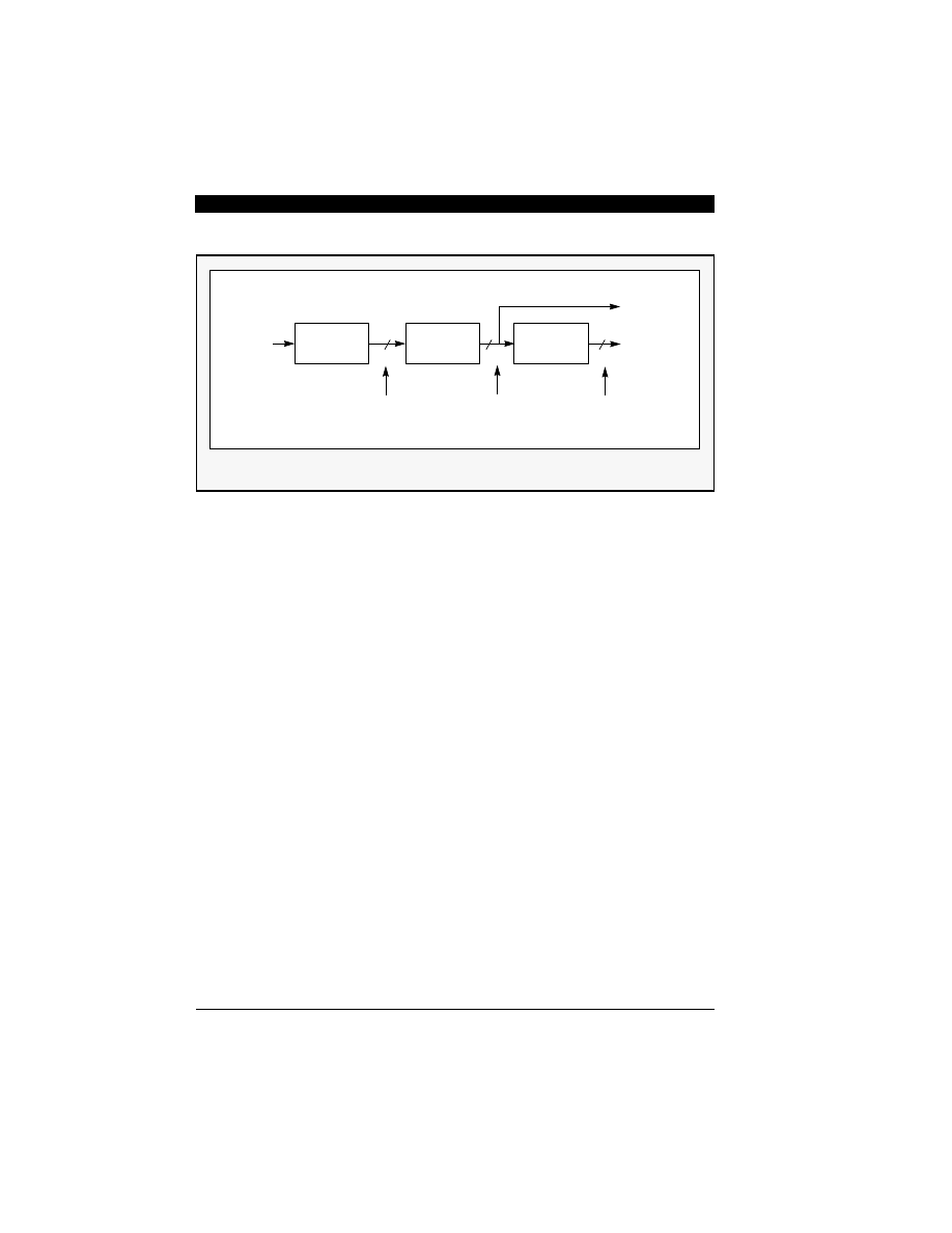
7.1 Comb-Filter Design as
a Decimator
A comb-filter of length N is a FIR filter with all N co-
efficients equal to one. The transfer function of a
comb-filter is:
Eqn. 7-1
Eqn. 7-2
Clearly the filter is a simple accumulator which
performs a moving average. Using the formula for
a geometric sum Eqn. 7-1 can be expressed in
closed form as:
Eqn. 7-3
or, in the discrete-time domain for N = 4:
Eqn. 7-4
Using this recursive form the number of additions
has been reduced to become independent of N.
The closed form solution in Eqn. 7-3 can be fac-
tored into two separate processes-integration
followed by differentiation as shown in Eqn. 7-5 :
Eqn. 7-5
H z
( )
z
n
–
n
0
=
N 1
–
∑
Y z
( )
X z
( )
-----------
=
=
y n
( )
x n
( )
x n
1
–
(
)
x n
2
–
(
)
x n
3
–
(
)
+
+
+
=
H z
( )
1
z
N
–
–
1
z
1
–
–
------------------
Y z
( )
X z
( )
-----------
=
=
y n
( )
x n
( )
x n
4
–
(
)
–
y n
1
–
(
)
+
=
y z
( )
1
1
z
1
–
–
-----------------
1
z
N
–
–
[
]
x z
( )
=
7-6
MOTOROLA
Now, since the comb filter will be followed by an N:1
decimator, the differentiation function can be done at
the lower rate. This discussion for a general N:1
comb-filter decimator is shown in Figure 7-2. Note
that the accumulator can overflow however, as long
as the final output does not overflow (i.e., the filter is
scaled properly for unity gain) and two’s complement
or
“wrap around” arithmetic is used, the accumulator
overflow will not cause an error [18,19].
The transfer function and magnitude response of a
comb-filter with the filter window length N = 16 fol-
lowed by a 16:1 decimation process are shown in
Figure 7-3. In summary the comb-filter decimator
has the following advantages:
• no multipliers are required
• no storage is required for filter coefficients
• intermediate storage is reduced by integrating
at the high sampling rate and differentiating at
the low sampling rate, compared to the
equivalent implementation using cascaded
uniform FIR filters
• the structure of comb-filters is very “regular”
consisting of two basic building blocks
• little external control or complicated local timing
is required
Figure 7-2 Block Diagram of One-Stage Comb Filtering Process
F
s
F
s
F
s
/N
F
s
/N
Differentiator
Output
sample rate
Input
sample rate
Integrator Decimation
1
1
z 1
–
–
------------------
N : 1
1
z 1
–
–

MOTOROLA
7-7
• the same filter design can easily be used for a
wide range of rate change factors, N, with the
addition of a scaling circuit and minimal
changes to the filter timing
A single comb-filter stage usually does not have
enough stop-band attenuation in the region of inter-
est to prevent aliasing after decimation. However,
cascaded comb-filters can be used to give enough
stop-band attenuation. Figure 7-4 shows a struc-
ture of four cascaded comb filter sections and the
resulting spectrum compared to lower order comb-fil-
ter stages. This realization needs eight registers for
data and 4(N+1) additions per input for computation.
400k
800k
1200k
1600k
-10
-20
-30
-40
0
dB
frequency
y n
( )
x n
i
–
(
)
i
0
=
15
∑
=
Y z
( )
1
z 16
–
–
1
z 1
–
–
---------------------
X z
( )
=
: Moving Average Process
Figure 7-3 Transfer Function of a Comb-Filter
No Multiplications
No Coefficient Storage
Linear Phase
7-8
MOTOROLA
There are considerable advantages in both storage
and arithmetic for this kind of comb decimator realiza-
tion. This approach is also attractive because the
comb decimation filter delivers not only a much faster
sample rate with 12 bits of dynamic resolution, but
also an untruncated or arithmetically undistorted 16-bit
output. SECTION 8 discusses an application which
takes advantage of this comb-filter output.
Figure 7-4 Cascaded Structure of a Comb-Filter
F
s
F
s
/N
1
1
z 1
–
–
----------------
N : 1
1
z 1
–
–
1
1
z 1
–
–
----------------
1
1
z 1
–
–
----------------
1
z 1
–
–
1
z 1
–
–
1
z 1
–
–
1
1
z 1
–
–
----------------
Four Integers
Decimation
Four Differentiators
MOTOROLA
7-9
Figure 7-5 Aliased Noise in Comb-Filter Output
0
500
1000
2000
2500
3200
1500
frequency in kHz
0
-60
-100
-140
-20
0
500
1000
2000
2500
3200
1500
0
-60
-100
-140
-20
frequency in kHz
frequency in kHz
0
500
1000
2000
2500
3200
1500
0
-60
-100
-140
-20
(a) Noise Spectrum of 1-Bit Input to comb Filter
(b) Spectrum of 4-Stage Comb Filter
(c) Noise Spectrum of 16-bit Comb Filter Output
(-72 dB Noise Power: 12-bit Dynamic Resolution)

7-10
MOTOROLA
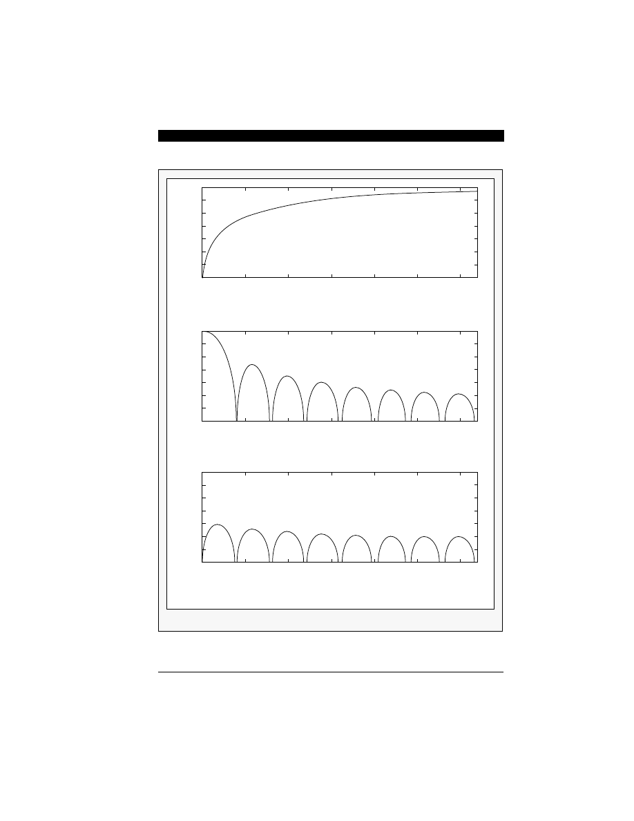
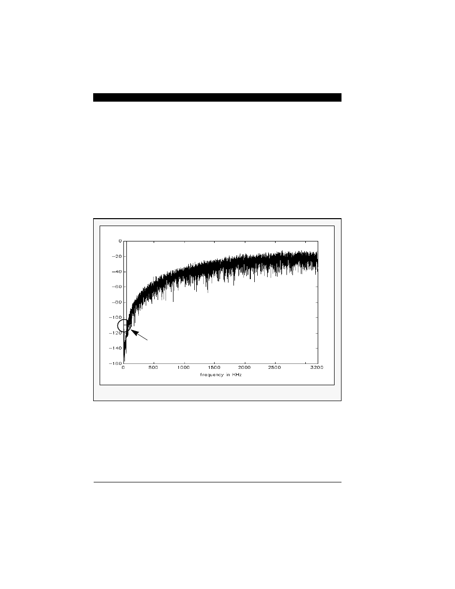
Figure 7-5(a) shows the third-order
Σ−∆
noise shaper
output spectrum; the four-stage comb-filter magnitude
response is illustrated in Figure 7-5(b). Thus, the theo-
retical quantized noise filtered by the four-stage comb-
filter can be computed as shown in Figure 7-5(c). After
a 16:1 decimation process, the noise in the frequency
band from 200 kHz to 1.6MHz will be aliased back to
baseband of up to 200 kHz. The numerical summation
of total noise in Figure 7-5(c) is around -72 dB S/N ratio
which yields a linear 12-bit dynamic resolution.
7.2 Second Section
Decimation FIR Filter
The first comb-filter section decimates the
Σ−∆
modulator output to the intermediate rate of 400
kHz (assuming a master clock at 12.8 MHz) and
the second filter section provides the sharp filter-
ing necessary to reduce the frequency aliasing
effect when the sampling rate is decimated down
to 100 kHz while the resolution becomes 16 bit.
The second filter section has two different tasks to
perform. The first task is 4:1 decimation lowpass
filtering with 0.001 dB ripple up to 45.5 kHz and
more than -96 dB cutoff attenuation above 50 kHz.
The stop-band attenuation of -96 dB is sufficient be-
cause the quantization noise level has not yet
reached its full magnitude as shown in Figure 6-10(c).
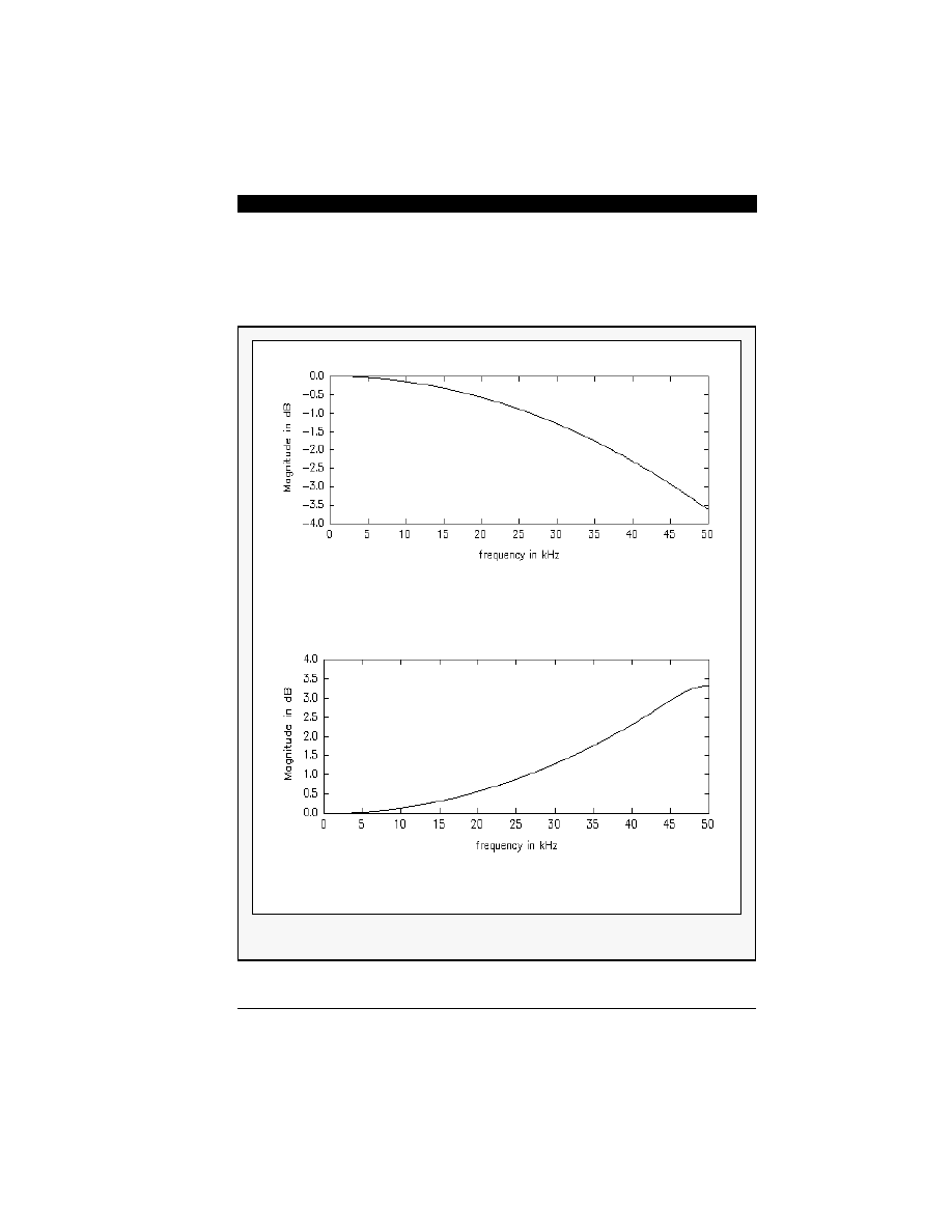
The second task is the passband response compen-
sation for the droop introduced by the
“comb-filter”
section. Figure 7-6(a) shows the magnitude droop
MOTOROLA
7-11
by the fourth order cascaded comb filter section,
while Figure 7-6(b) shows the compensation filter re-
sponse up to cutout frequency.
(b) Compensation FIR Filter Magnitude Response
(a) Comb-Filter Magnitude Response in Baseband
Figure 7-6 Magnitude Response
7-12
MOTOROLA
Although FIR filters take more time to perform the
decimation filtering process than infinite impulse
response (IIR) filters for the same passband and
out-of-band frequency characteristics, FIR filters
can be designed to have a linear-phase response
which is required for high-end audio and instru-
mentation applications.
Design techniques for calculating the FIR filter
coefficients with linear-phase response are well
documented [5,20]. Figure 7-7 shows the frequency
response of a low-pass FIR filter with 255 symmetric
coefficients using a computer optimized procedure.
This filter provides a stop-band attenuation of -96 dB
with a maximum passband ripple of 0.001dB which
meets the filter requirement as defined in the
DSP56ADC16 datasheet [21]. However, the
Figure 7-7 FIR Filter Magnitude Response
0.0005 dB
passband
ripple
MOTOROLA
7-13
actual second section FIR filter coefficients are
computed by the combination of the compensation
filter and the lowpass filter.
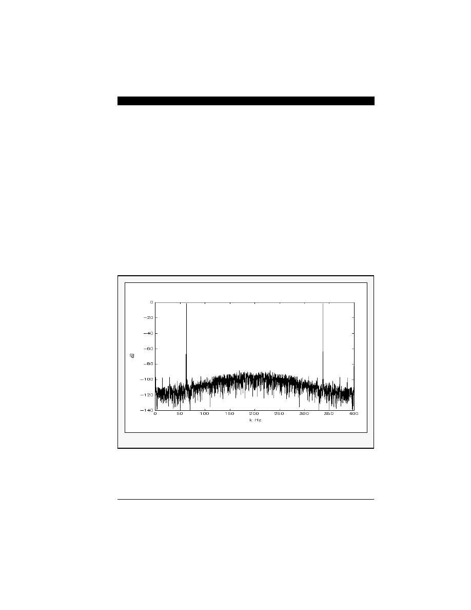
Figure 7-8 shows the frequency bands and the fi-
nal quantized noise level which would have
aliased back to baseband after 64:1 decimation
by the comb-filter section and the second 4:1
decimation section. When the one-pole RC ana-
log lowpass filter is implemented at the analog
input terminals as discussed in SECTION 4, the
power of the aliased frequency band shown in
Figure 7-8 will be less than -96 dB. In fact, the
theoretical and numerical computations show
that total aliased power after the final decimation
process is around -110 dB S/N ratio.
■
Figure 7-8 Aliased Noise Bands of FIR Filter Output
aliased frequency bands
: 4-Stage Comb + FIR Filter
0
200
400
600
800
1000
1200
1400
1600
0
-10
-20
-30
-40
-50
-60
-70
-80
-90
-100
Magnitude (dB)
Frequency (kHz)

7-14
MOTOROLA

MOTOROLA
8-1
Mode Resolution by
Filtering the Comb-
Filter Output with
Half-Band Filters
SECTION 8
T
his section explains how to obtain 18-20 bit resolu-
tion from the comb-filter output. In particular, a series
half-band filter structure is suggested to take advan-
tage of a third-order noise-shaper combined with
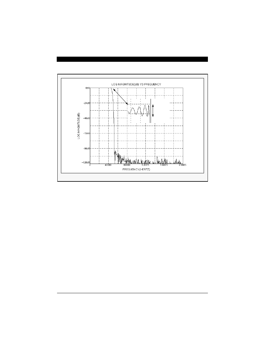
oversampling. Figure 8-1 shows the spectrum of a
third-order noise-shaper whose input-output equation
is defined in Eqn. 6-8. The transfer function (1 - z
-1
)
3
in Eqn. 6-8 for the quantization noise is essentially a
highpass filter so that the noise is shifted to higher,
out-of-band, frequencies where it is then digitally fil-
tered out.
At the final arithmetic operation for the FIR filter out-
put, a 38-bit accumulator value is convergently
rounded to fit into the 16-bit output data format. Thus,
the shaped noise shown in Figure 8-1 becomes al-
most flat at the 16-bit level due to the arithmetic
rounding noise. Although the comb-filter output has
only 12-bit resolution, the 16-bit output value is not yet
arithmetically rounded or truncated. Thus, the input
“The half-band
filter is based on
a symmetrical
FIR design and
approximately
half of the filter
coefficients are
exactly zero.
Hence, the
number of
multiplications
in implementing
such filters is
one-fourth of that
needed for
arbitrary FIR
filter designs.”
8-2
MOTOROLA
signal and the baseband spectral shape of the
third-order noise shaper are unchanged, as shown
in Figure 8-2. Since the comb-filter is designed to
obtain maximum attenuation only on the higher fre-
quency components which will be aliased into the
frequency band of interest after 16:1 decimation
[18], the characteristic of the analog input signal is
preserved, while the out-of-band shaped noise
shown in Figure 8-1 has been attenuated.
The output from most conventional converters in-
cluding the FIR filter output of the DSP56ADC16,
has a flat background noise due to the quantization
noise as well as arithmetic rounding noise. Thus,
further decimation processes can only gain 3 dB or
Figure 8-1 Spectrum of a Third-Order Noise Shaper (16384 FFT bins)
flat response due to the FIR filter arithmetic rounding
power in dB
MOTOROLA
8-3
1/2 bit more resolution per octave. In other words,
a further 16:1 or 256:1 decimation process of the
16-bit resolution output signal is required to obtain
18-bit resolution at 6.25 kHz sample rate or 20-bit
resolution at 400 Hz sample rate, respectively,
which is very impractical. By taking advantage of
the fact that the noise is shaped in the comb-filter
output, 9 dB or 1.5 bit more resolution per octave
can be theoretically achieved. Thus, a further 16:1
or 64:1 decimation process can provide 18-bit res-
olution at 25 kHz sample rate or 20-bit resolution at
6.25 kHz sample rate, respectively. (This assumes
quantization noise is dominant.)
Figure 8-2 Spectrum of Typical Comb-Filter Output (4096 FFT bins)
8-4
MOTOROLA
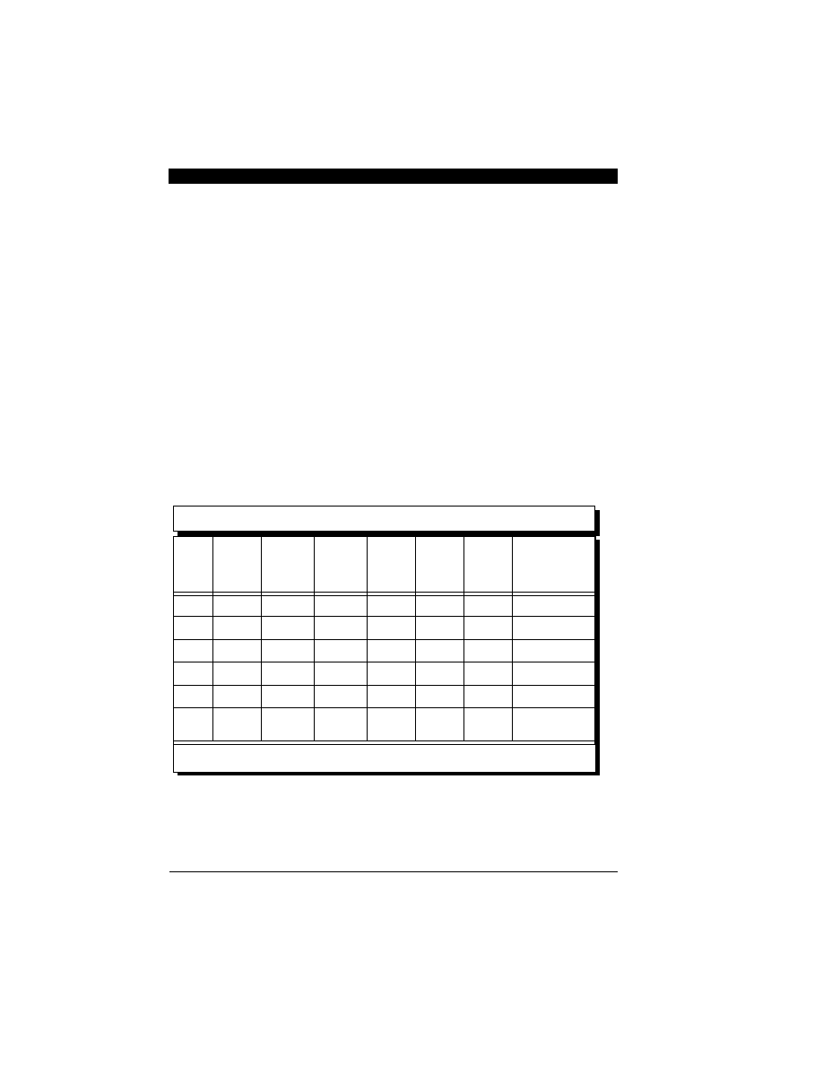
Figure 8-3 illustrates the cascaded half-band filter
design specification for a 64:1 decimation process.
The number of instructions to run the filters on the
DSP56001 and the memory requirements are tabu-
lated in Table 8-1. A cascaded half-band filter
structure is used for computational simplicity [22].
The half-band filter is based on a symmetrical FIR
design and approximately half of the filter coeffi-
cients are exactly zero. Hence, the number of
multiplications in implementing such filters is one-
fourth of that needed for arbitrary FIR filter designs.
Since a half-band filter can only implement a 2:1
decimation, a series of such filters may be cascad-
ed to perform a higher decimation filter process.
Table 8-1 Parameters for Designing Half-Band Filters
Stage
Output
sample
rate
Passband Stopband # of taps
# of coef
in RAM
# of
MAC
# of instructions
per second
1
200k
3k
197k
19
6
11
11x200k=2.2M
2
100k
3k
97k
19
6
11
11x100k=1.1M
3
50k
3k
47k
19
6
11
11x50k=550K
4
25k
3k
22k
23
7
13
13x25k=325K
5
12.5k
3k
9.5k
31
9
17
17x12.5k=212.5K
6
6.25k
2.9k
3.55k
199
51
99
99x6.25k=618.75
K
Total number of instructions for 6 half-band filters per second : 5.007 MIPS

MOTOROLA
8-5
To obtain more than a 16-bit resolution signal output,
a processor with more than 16-bit coefficient word-
width is required. Fortunately, the DSP56001 gener-
al purpose DSP processor has a hardware multiply-
accumulate unit that is able to multiply 24-bit data
and 24-bit coefficient, and accumulate 56 bits in just
one instruction, which is useful for half-band filter op-
erations. The DSP56001 architecture also
provides parallel data buses, circular buffers, and
large on-chip memories along with a 75 ns instruc-
tion cycle, which fits nicely for the proposed filter
structure [23]. Detailed discussion on this topic
can be found in [24].
■
200k
100k
50k
25k
6.25k
12.5k
Stage 1
Stage 2
Stage 3
Stage 4
Stage 5
Stage 6
3k
3.125k
3k
3k
3k
3k
400k
200k
100k
50k
25k
12.5k
Figure 8-3 Decimation Process using a Series of Half-Band Filters


MOTOROLA
9-1
SECTION 9
S
igma-Delta conversion technology is based on
oversampling, noise shaping, and decimation filtering.
There are many inherent advantages in
Σ−∆
based
analog-to-digital converters. The major advantage be-
ing that it is based predominantly on digital signal
processing, hence the cost of implementation is low
and will continue to decrease. Also, due to its digital
nature
Σ−∆
converters can be integrated onto other
digital devices. Manufacturing technology notwith-
standing,
Σ−∆
technology offers system cost savings
because the analog anti-aliasing filter requirements
are considerably less complex and the sample-and-
hold circuit is intrinsic to the technology due to the high
input sampling rate and the low precision A/D conver-
sion. Since the digital filtering stages reside behind the
A/D conversion, noise injected during the conversion
process, such as power-supply ripple, voltage-refer-
ence noise, or noise in the ADC itself, can be
controlled. Also,
Σ−∆
converters are inherently linear
and don’t suffer from appreciable differential non-lin-
earity, and the background noise level which sets the
system S/N ratio is independent of the input signal lev-
el. The last, but certainly not least, consideration is
cost. Attaining a high level of performance at a fraction
of the cost of hybrid and modular designs is probably
the greatest advantage of all.
■
Summary
“. . .
Σ−∆
technology offers
system cost
savings because
the analog anti-
aliasing filter
requirements
are considerably
less complex . . .”


MOTOROLA
References-1
REFERENCES
[1]
H. Inose, Y. Yasuda and J. Marakami, “A teleme-
tering system by code modulation, delta-sigma
modulation,”
IRE Trans. on Space, Electronics
and Telemetry, SET-8, pp. 204-209, Sept. 1962.
[2] H. Nyquist, “Certain topics in telegraph transmis-
sion theory,”
AIEE Trans., pp. 617-644, 1928.
[3] M. Armstrong, et al, “A COMS programmable
self-calibrating 13b eight-channel analog inter-
face processor,”
ISSCC Dig. Tech. Paper, pp.
44-45, Feb. 1987.
[4] K. Lakshmikumar, R. Hadaway, and M. Cope-
land, “Characterization and modeling of
mismatch in MOS transistors for precision ana-
log design,”
IEEE J. Solid-State Circuits, Vol.
SC-21, pp. 1057-1066, Dec. 1986.
[5] N. Ahmed and T. Natarajan,
Discrete-Time Sig-
nals and Systems, Prentice-Hall, Englewood
Cliffs, NJ, 1983.
[6] R.
Steele,
Delta Modulation Systems, Pentech
Press, London, England, 1975.
[7] N. Scheinberg and D. Schilling, “Techniques for
correcting transmission error in video adaptive
delta-modulation channels,”
IEEE Trans. Com-
mun., pp. 1064-1070, Sept. 1977.
[8] Y. Matsuya, et al, “A 16 bit oversampling A-to-D
conversion technology using triple-integration
noise shaping,”
IEEE J. of Solid-State Circuits,
Vol. SC-22, No. 6, pp. 921-929, Dec. 1987.

References-2
MOTOROLA
[9] M. Rebeschini et al, “A high-resolution CMOS
Sigma-Delta A/D converter with 320 kHz out-
put rate,”
Proc. ISCAS, pp. 246-249, 1989.
[10] C. D. Thompson, “A VLSI sigma delta A/D con-
verter for audio and signal processing
applications,”
Proc. Int. Conf. on Acoustic,
Speech and Signal Processing, Vol. 4. pp. 2569-
2572, Glasgow, Scotland, May 23-26, 1989.
[11] J. C. Candy, “A use of double integration in
Sigma-Delta modulation,”
IEEE Trans. on
Communications, Vol. COM-33, No. 3, pp.
249-258, March 1985.
[12] R. Koch, et al, “A 12-bit Sigma-Delta analog-
to-digital converter with a 15-MHz clock rate,”
IEEE J. of Solid-State Circuits, Vol. SC-21, No.
6, pp. 1003-1010, Dec. 1986.
[13] B. Boser and B. Wooley, “Quantization error
spectrum of Sigma-Delta modulators,”
Proc.
International Symposium on Circuits and Sys-
tems, pp. 2331-2334, June, 1988.
[14] W. L. Lee and C. G. Sodini, “A topology for
higher order interpolative coders,”
Proc. Inter-
national Symposium on Circuits and Systems,
pp. 459-462, May 1987.
[15] D. R. Welland, et al, “A stereo 16-bit delta-sigma
A/D converter for digital audio,”
Proc. the 85th
convention of Audio Engineering Society, Vol.
2724 (H-12), Los Angeles, CA, Nov. 3-6, 1988.
[16] W. Bennett, “Spectra of quantized signals,”
Bell Syst. Tech. J., Vol. BSTJ-27, pp. 446-472,
July 1948.

MOTOROLA
References-3
[17] B. Widrow, “A study of rough amplitude quan-
tization by means of Nyquist sampling theory,”
IRE Trans. Circuit Theory, Vol. CT-3, pp. 266-
276, Dec. 1956.
[18] E. B. Hogenauer, “An economical class of dig-
ital filters for decimation and interpolation,”,
IEEE Trans, Acoust. Speech Signal Process.,
Vol. ASSP-29, No. 2, pp. 155-162, April 1981.
[19] S. Chu and C. S. Burrus, “Multirate filter de-
signs using comb filters,”
IEEE Trans. on
Circuits and Systems, Vol. CAS-31, No. 11,
pp. 913-924, Nov. 1984.
[20] A. V. Oppenheim and R. W. Schafer,
Discrete-
time signal processing, Prentice-Hall, Engle-
wood Cliffs, NJ, 1989.
[21] Motorola Inc.,
DSP56ADC16 Technical Data
Sheet (DSP56ADC16/D), 1989.
[22] R. E. Crochiere and L. R. Rabiner,
Multirate
Digital Signal Processing, Prentice-Hall, En-
glewood Cliffs, NJ, 1983.
[23] Motorola Inc.,
DSP56000/DSP56001 Digital
Signal Processor User’s Manual, Rev. 2, 1990.
[24] S. Park, “A real-time implementation of half-
band filters to obtain 18-20 bit resolution from
the DSP56ADC16 Sigma-Delta A/D convert-
er,”
Proc. International Conference on
Acoustics, Speech and Signal Processing,
Vol. 2. pp. 989-992, Albuquerque, NM, April 3-
6, 1990.
■

Document Outline
- Cover
- Motorola Digital Signal Processors
- Table of Contents
- List of Illustrations
- List of Tables
- Introduction
- Conventional Analog-to-Digital Converters
- Quantization Error in A/D Conversion
- Oversampling and
- Delta Modulation
- Sigma-Delta Modulation and Noise Shaping
- Digital Decimation Filtering
- Mode Resolution by Filtering the Comb-Filter Output with Half-Band Filters
- Summary
- References
Wyszukiwarka
Podobne podstrony:
Principles of Sigma Delta Conversion for Analog to Digital Converters
Applications of polyphase filters for bandpass sigma delta analog to digital conversion
Applications of polyphase filters for bandpass sigma delta analog to digital conversion
Development Of High Frequency Link Direct Dc To Ac Converters For Link Direct Dc To Ac Converters Fo
Przetwornik analogowo cyfrowy typu sigma delta
Język angielski What do you think of AIDS victims?gging for money to live
Applying Principles of Neurodevelopment to Clinical Work with Maltreated and Traumatized Children
Applying Principles of Neurodevelopment to Clinical Work with Maltreated and Traumatized Children
Accounting Recording and Firm Reporting as Source of Information for Users to Take Economic Decision
Overview of bacterial expression systems for heterologous protein production from molecular and bioc
The Code of Honor or Rules for the Government of Principals and Seconds in Duelling by John Lyde Wil
Design and construction of three phase transformer for a 1 kW multi level converter
0791459012 State University of New York Press Kant on Causation On the Fivefold Routes to the Princi
Haisch Update on an Electromagnetic Basis for Inertia, Gravitation, Principle of Equivalence, Spin
Basic Principles Of Perspective Drawing For The Technical Illustrator
Heron, Shapira (2003) Time to log of New diagnostic criteria for problematic Internet use
Keith Mitchell Sacks of Cash [Proven Ways For Average People To Create Income From Virtually Nothin
więcej podobnych podstron