Data Brief
For further information contact your local STMicroelectronics sales office.
August 2008
Rev 1
1/49
49
AIS326DQ
MEMS inertial sensor
3-axis, low g accelerometer with digital output
Features
■
3.3 V single supply operation
■
1.8 V compatible IOs
■
SPI digital output interface
(a)
■
12 bit resolution
■
Interrupt activated by motion
■
Programmable interrupt threshold
■
Embedded self-test
■
High shock survivability
■
ECOPACK
®
compliant (see
■
Extended temperature range -40 °C to +105 °C
Description
The AIS326DQ is a three axes digital output
accelerometer that includes a sensing element
and an IC interface able to take the information
from the sensing element and to provide the
measured acceleration signals to the external
world through an SPI serial interface.
The sensing element, capable of detecting the
acceleration, is manufactured using a dedicated
process developed by ST to produce inertial
sensors and actuators in silicon.
The IC interface instead is manufactured using a
CMOS process that allows high level of
integration to design a dedicated circuit which is
factory trimmed to better match the sensing
element characteristics.
The AIS326DQ has a user selectable full scale of
±2 g, ±6 g and it is capable of measuring
acceleration over a bandwidth of 640 Hz for all
axes. The device bandwidth may be selected
accordingly to the application requirements. The
self-test capability allows the user to check the
functioning of the system.
The device is available in plastic quad flat
package no lead surface mount (QFPN) and it is
specified over a temperature range extending
from -40 °C to +105 °C.
The AIS326DQ may be used in non-safety
automotive applications, such as:
■
Anti-theft systems and inertial navigation
■
Motion activated functions
■
Vibration monitoring and compensation
■
Tilt measurements
■
Black boxes, event recorders
a.
I
2
C interface is also available.
QFPN-28
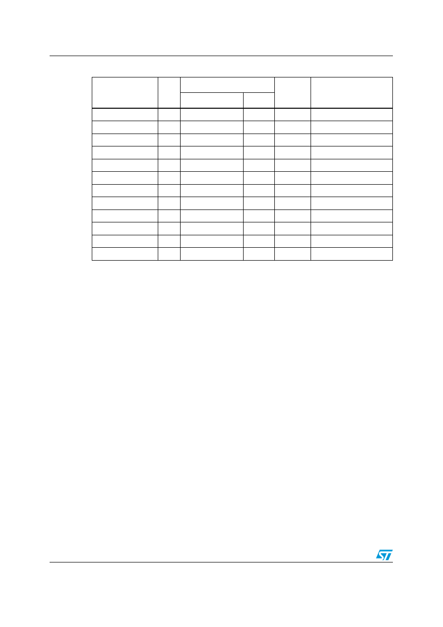
Table 1.
Device summary
Order code
Operating temperature
range [
° C]
Package
Packing
AIS326DQ
-40 to +105
QFPN-28
Tray
AIS326DQTR
-40 to +105
QFPN-28
Tape and reel

Contents
AIS326DQ
2/49
Contents
Block diagram and pin description . . . . . . . . . . . . . . . . . . . . . . . . . . . . . 8
Mechanical and electrical specifications . . . . . . . . . . . . . . . . . . . . . . . 10
Communication interface characteristics . . . . . . . . . . . . . . . . . . . . . . . . . 13
SPI - serial peripheral interface . . . . . . . . . . . . . . . . . . . . . . . . . . . . . . . 13
Absolute maximum ratings . . . . . . . . . . . . . . . . . . . . . . . . . . . . . . . . . . . . 14
SPI Read . . . . . . . . . . . . . . . . . . . . . . . . . . . . . . . . . . . . . . . . . . . . . . . . 20
SPI Write . . . . . . . . . . . . . . . . . . . . . . . . . . . . . . . . . . . . . . . . . . . . . . . . 21
SPI Read in 3-wires mode . . . . . . . . . . . . . . . . . . . . . . . . . . . . . . . . . . . 22

AIS326DQ
Contents
3/49
HP_FILTER_RESET (23h) . . . . . . . . . . . . . . . . . . . . . . . . . . . . . . . . . . . . 29
FF_WU_CFG (30h) . . . . . . . . . . . . . . . . . . . . . . . . . . . . . . . . . . . . . . . . . 33
FF_WU_SRC (31h) . . . . . . . . . . . . . . . . . . . . . . . . . . . . . . . . . . . . . . . . . 34
FF_WU_ACK (32h) . . . . . . . . . . . . . . . . . . . . . . . . . . . . . . . . . . . . . . . . . 34
FF_WU_THS_L (34h) . . . . . . . . . . . . . . . . . . . . . . . . . . . . . . . . . . . . . . . 34
FF_WU_THS_H (35h) . . . . . . . . . . . . . . . . . . . . . . . . . . . . . . . . . . . . . . . 34
FF_WU_DURATION (36h) . . . . . . . . . . . . . . . . . . . . . . . . . . . . . . . . . . . . 35
DD_THSE_H (3Fh) . . . . . . . . . . . . . . . . . . . . . . . . . . . . . . . . . . . . . . . . . 37

Contents
AIS326DQ
4/49
Typical performance characteristics . . . . . . . . . . . . . . . . . . . . . . . . . . . 38
Mechanical characteristics at 25 °C . . . . . . . . . . . . . . . . . . . . . . . . . . . . . 38
Mechanical characteristics at -40 °C . . . . . . . . . . . . . . . . . . . . . . . . . . . . 39
Mechanical characteristics at 105 °C . . . . . . . . . . . . . . . . . . . . . . . . . . . . 40
Electro-mechanical characteristics at 25 °C . . . . . . . . . . . . . . . . . . . . . . . 42
Electrical characteristics at 25 °C . . . . . . . . . . . . . . . . . . . . . . . . . . . . . . . 43
Electrical characteristics at -40 °C . . . . . . . . . . . . . . . . . . . . . . . . . . . . . . 43
Electrical characteristics at 105 °C . . . . . . . . . . . . . . . . . . . . . . . . . . . . . . 43
General guidelines about soldering surface mount accelerometer . . . . . 44
Stencil design and solder paste application . . . . . . . . . . . . . . . . . . . . . . . 45

AIS326DQ
List of tables
5/49
List of tables
Mechanical characteristics @ Vdd = 3.3 V, T = -40 °C to 105 °C unless otherwise noted. 10
Electrical characteristics @ Vdd=3.3 V, T = -40 °C to 105 °C unless otherwise noted . . . 12

List of tables
AIS326DQ
6/49

AIS326DQ
List of figures
7/49
List of figures
SPI slave timing diagram (2) . . . . . . . . . . . . . . . . . . . . . . . . . . . . . . . . . . . . . . . . . . . . . . . 13
Read and write protocol . . . . . . . . . . . . . . . . . . . . . . . . . . . . . . . . . . . . . . . . . . . . . . . . . . . 19
SPI read protocol . . . . . . . . . . . . . . . . . . . . . . . . . . . . . . . . . . . . . . . . . . . . . . . . . . . . . . . . 20
SPI Write protocol . . . . . . . . . . . . . . . . . . . . . . . . . . . . . . . . . . . . . . . . . . . . . . . . . . . . . . . . 21
SPI read protocol in 3-wires mode . . . . . . . . . . . . . . . . . . . . . . . . . . . . . . . . . . . . . . . . . . . 22
Recommended land and solder mask design for QFPN packages. . . . . . . . . . . . . . . . . . . 45
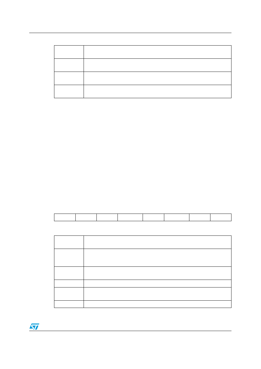
Block diagram and pin description
AIS326DQ
8/49
1
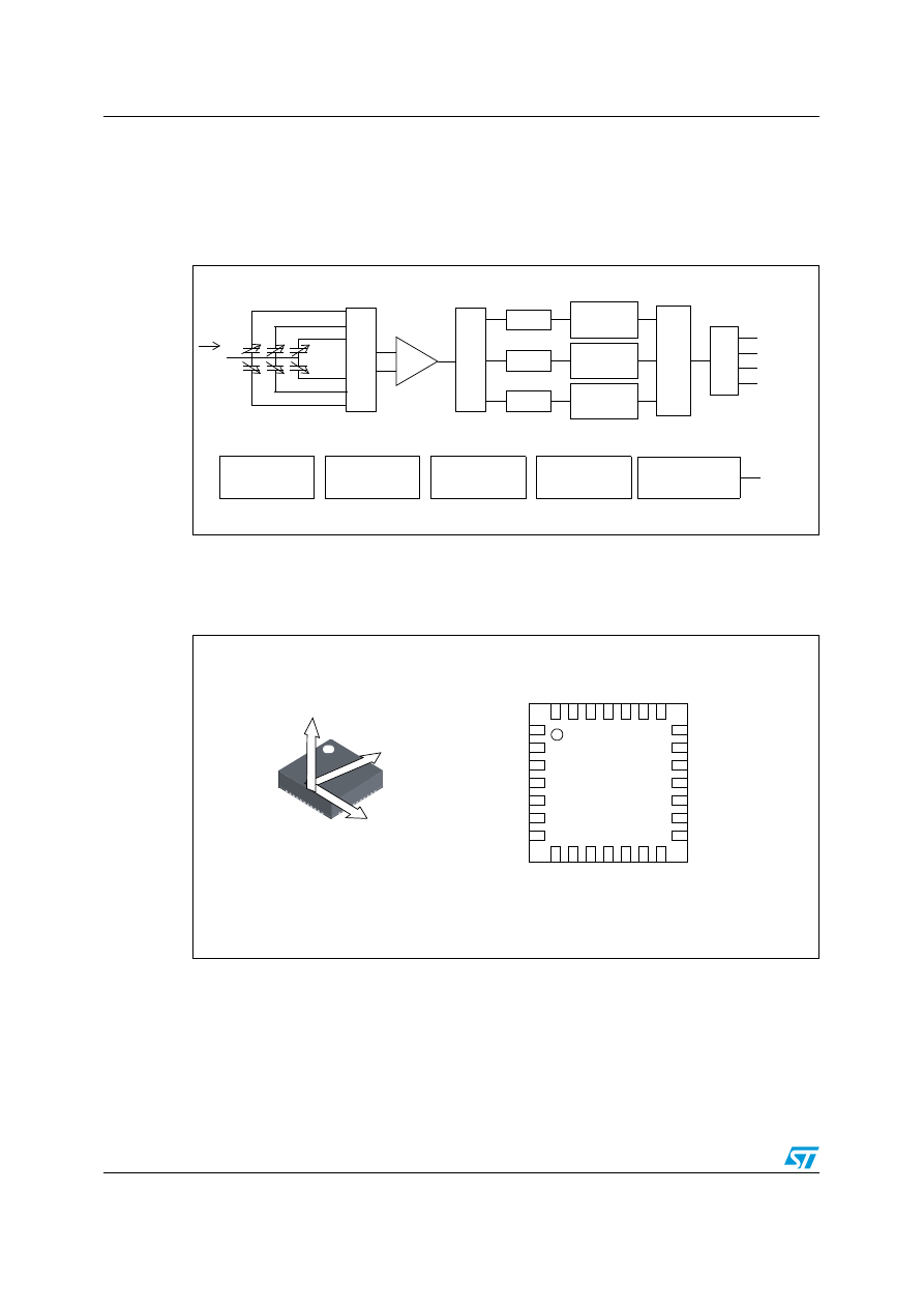
Block diagram and pin description
1.1 Block
diagram
Figure 1.
Block diagram
1.2 QFPN-28
pin
description
Figure 2.
Pin connection
Σ∆
CHARGE
AMPLIFIER
MUX
Y+
Z+
Y-
Z-
Regs
a
X+
X-
DE
MUX
Reconstruction
Filter
Σ∆
Σ∆
Array
SPI
CS
SPC
SDO/SDI
SDO
CONTROL LOGIC
&
INTERRUPT GEN.
RDY/INT
Reconstruction
Filter
Reconstruction
Filter
CLOCK
TRIMMING
CIRCUITS
REFERENCE
SELF TEST
AIS326DQ
NC
GND
Reserved
Vdd
GND
RDY/INT
NC
NC
Reserved
Reserved
Vdd
GND
CK
NC
NC
SD
O
Vdd
_
IO
S
D
I/S
DO
SP
C
CS
NC
NC
NC
NC
NC
NC
NC
NC
1
7
28
22
21
15
8
14
Y
1
X
Z
DIRECTIONS OF THE
DETECTABLE
ACCELERATIONS
(TOP VIEW)

AIS326DQ
Block diagram and pin description
9/49
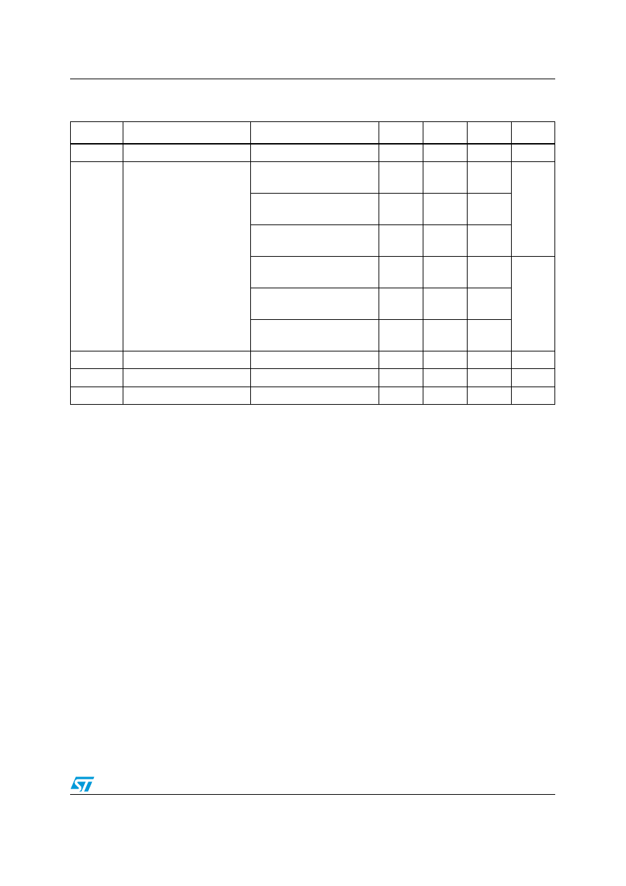
Table 2.
Pin description
Pin#
Name
Function
1
NC
Internally not connected
2
GND
0 V supply
3
Vdd
Power supply
4
Reserved
Either leave unconnected or connect to GND
5
GND
0 V supply
6
RDY/INT
Data ready/inertial wake-up and free-fall interrupt
7, 8
NC
Internally not connected
9
SDO
SPI serial data output
10
SDI/
SDO
SPI serial data input (SDI)
3-wire interface serial data output (SDO)
11
Vdd_IO
Power supply for I/O pads
12
SPC
SPI serial port clock
13
CS
Chip select (logic 0: SPI enabled, logic 1: SPI disabled)
14, 15
NC
Internally not connected
16
CK
Optional external clock, if not used either leave unconnected or
connect to GND
17
GND
0 V supply
18
Reserved
Either leave unconnected or connect to Vdd_IO
19
Vdd
Power supply
20
Reserved
Connect to Vdd
21 - 28
NC
Internally not connected

Mechanical and electrical specifications
AIS326DQ
10/49
2
Mechanical and electrical specifications
2.1 Mechanical
characteristics
Table 3.
Mechanical characteristics @ Vdd = 3.3 V, T = -40 °C to 105 °C unless otherwise
noted
(1)
Symbol
Parameter
Test conditions
Min.
Typ.
(2)
Max.
Unit
FS
Measurement range
(3)
FS bit set to 0
±1.7
±2.0
g
FS bit set to 1
±5.3
±6.0
Dres
Device resolution
Full-scale = ±2
g
T = 25 °C, ODR1=40 Hz
1.0
mg
Full-scale = ±2
g
T = 25 °C, ODR2=160 Hz
2.0
Full-scale = ±2
g
T = 25 °C, ODR3 = 640 Hz
3.9
Full-scale = ±2
g
T = 25 °C, ODR4 = 2560 Hz
15.6
So
Sensitivity
Full-scale = ±2
g
12 bit representation
952
1024
1096
LSb/g
Full-scale = ±6
g
12 bit representation
(4)
316
340
364
TCSo
Sensitivity change vs
temperature
Full-scale = ±2
g
12 bit representation
0.025
%/°C
Off
Zero-g level offset
accuracy
(5),(6)
Full-scale = ±2
g
X, Y axis
-100 100
mg
Full-scale = ±2
g
Z axis
-200
200
Full-scale = ±6
g
X, Y axis
(4)
-100
100
Full-scale = ±6
g
Z axis
(4)
-200
200
TCOff
Zero-g level change vs
temperature
Max delta from 25 °C
0.2
mg/°C
NL
Non linearity
(4)
Best fit straight line
X, Y axis
Full-scale = ±2
g
ODR = 40 Hz
±2
% FS
Best fit straight line
Z axis
Full-scale = ±2
g
ODR = 40 Hz
±3
AIS326DQ
Mechanical and electrical specifications
11/49
CrAx
Cross axis
(4)
-5
5
%
V
st
Self-test output change
(7),(8)
Full-scale= ±2
g
X axis
110
210
310
LSb
Full-scale= ±2
g
Y axis
110
210
310
Full-scale= ±2
g
Z axis
70
160
250
Full-scale= ±6
g
X axis
30
70
120
LSb
Full-scale= ±6
g
Y axis
30
70
120
Full-scale= ±6
g
Z axis
20
55
110
BW
System bandwidth
(9)
ODRx/4
Hz
T
OP
Operating temperature range
-40
+105
°C
Wh
Product weight
0.2
gram
1.
The product is factory calibrated at 3.3 V. Operation over 3.6 V is not recommended
2.
Typical specifications are not guaranteed
3.
Verified by wafer level test and specification of initial offset and sensitivity
4.
Guaranteed by design
5.
Zero-g level offset value after MSL3 preconditioning
6.
Offset can be eliminated by enabling the built-in high pass filter (HPF)
7.
Self test output changes with the power supply. “Self-test output change” is defined as OUTPUT[LSb]
(Self-test bit on
CTRL_REG1=1)
- OUTPUT[LSb]
(Self-test bit on CTRL_REG1=0)
. 1LSb = 1g/1024 at 12 bit representation, 2 g Full-scale
8.
Output data reach 99% of final value after 5/ODR when enabling Self-test mode due to device filtering
9.
ODRx is output data rate. Refer to
Table 3.
Mechanical characteristics @ Vdd = 3.3 V, T = -40 °C to 105 °C unless otherwise
noted
(1)
(continued)
Symbol
Parameter
Test conditions
Min.
Typ.
(2)
Max.
Unit
Mechanical and electrical specifications
AIS326DQ
12/49
2.2 Electrical
characteristics
Table 4.
Electrical characteristics @ Vdd=3.3 V, T = -40 °C to 105 °C unless otherwise noted
(1)
Symbol
Parameter
Test conditions
Min.
Typ.
(2)
Max.
Unit
Vdd
Supply voltage
3.0
3.3
3.6
V
Vdd_IO
I/O pads supply voltage
(3)
1.71
Vdd
V
Idd
Supply current
Vdd = 3.3 V
0.67
0.80
mA
IddPdn
Current consumption
in power-down mode
2
10
µA
VIH
Digital high level Input voltage
(3)
0.8*Vdd_IO
V
VIL
Digital low level Input voltage
(3)
0.2*Vdd_IO
VOH
High level output voltage
(3)
0.9*Vdd_IO
V
VOL
Low level output voltage
(3)
0.1*Vdd_IO
ODR1
Output data rate 1
Dec factor = 512
40
Hz
ODR2
Output data rate 2
Dec factor = 128
160
ODR3
Output data rate 3
Dec factor = 32
640
ODR4
Output data rate 4
Dec factor = 8
2560
BW
System bandwidth
(4)
ODRx/4
Hz
Ton
Turn-on time
(5)
5/ODRx
s
T
OP
Operating temperature range
-40
+105
°C
1.
The product is factory calibrated at 3.3 V. Operation over 3.6 V is not recommended
2.
Typical specifications are not guaranteed
3.
Guaranteed by design
4.
Digital filter -3 dB frequency
5.
Time to obtain valid data after exiting power-down mode
AIS326DQ
Mechanical and electrical specifications
13/49
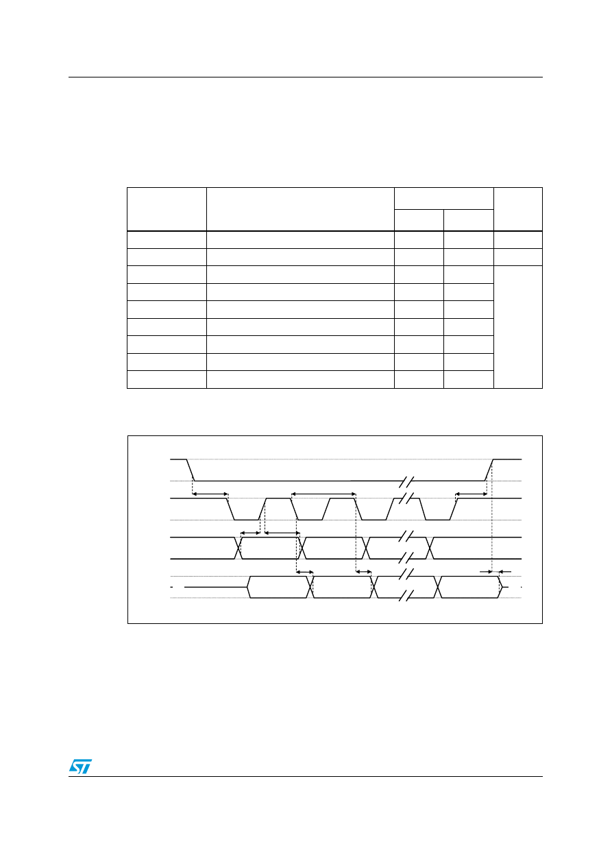
2.3
Communication interface characteristics
2.3.1
SPI - serial peripheral interface
Subject to general operating conditions for Vdd and T
OP
.
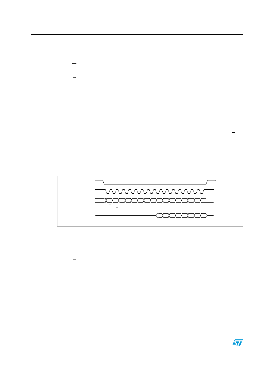
Figure 3.
SPI slave timing diagram
(2)
2.
Measurement points are done at 0.2·Vdd_IO and 0.8·Vdd_IO, for both input and output port
3.
When no communication is on-going, data on CS, SPC, SDI and SDO are driven by internal pull-up
resistors
Table 5.
SPI slave timing values
Symbol
Parameter
Value
(1)
1.
Values are guaranteed at 8 MHz clock frequency for SPI with both 4 and 3 wires, based on characterization
results, not tested in production
Unit
Min
Max
tc(SPC)
SPI clock cycle
125
ns
fc(SPC)
SPI clock frequency
8
MHz
tsu(CS)
CS setup time
5
ns
th(CS)
CS hold time
10
tsu(SI)
SDI input setup time
5
th(SI)
SDI input hold time
15
tv(SO)
SDO valid output time
55
th(SO)
SDO output hold time
7
tdis(SO)
SDO output disable time
50
SPC
CS
SDI
SDO
t
su(CS)
t
v(SO)
t
h(SO)
t
h(SI)
t
su(SI)
t
h(CS)
t
dis(SO)
t
c(SPC)
MSB IN
MSB OUT
LSB OUT
LSB IN
(3)
(3)
(3)
(3)
(3)
(3)
(3)
(3)
Mechanical and electrical specifications
AIS326DQ
14/49
2.4
Absolute maximum ratings
Stresses above those listed as “absolute maximum ratings” may cause permanent damage
to the device. This is a stress rating only and functional operation of the device under these
conditions is not implied. Exposure to maximum rating conditions for extended periods may
affect device reliability.
This is a mechanical shock sensitive device, improper handling can cause
permanent damages to the part
This is an ESD sensitive device, improper handling can cause permanent damages
to the part
Table 6.
Absolute maximum ratings
Symbol
Ratings
Maximum value
Unit
Vdd
Supply voltage
(1)
1.
Supply voltage on any pin should never exceed 6.0 V.
-0.3 to 6.0
V
Vdd_IO
I/O pins supply voltage
(1)
-0.3 to Vdd +0.1
V
Vin
Input voltage on any control pin
(1)
(CS, SPC, SDI/SDO, SDO, CK)
-0.3 to Vdd_IO +0.3
V
A
POW
Acceleration (any axis, powered, Vdd = 3.3 V)
3000
g for 0.5 ms
10000
g for 0.1 ms
A
UNP
Acceleration (any axis, unpowered)
3000
g for 0.5 ms
10000
g for 0.1 ms
T
OP
Operating temperature range
-40 to +105
°C
T
STG
Storage temperature range
-40 to +125
°C
ESD
Electrostatic discharge protection
4.0 (HBM)
kV
200 (MM)
V
1.5 (CDM)
kV

AIS326DQ
Mechanical and electrical specifications
15/49
2.5 Terminology
2.5.1 Sensitivity
Sensitivity describes the gain of the sensor and can be determined e.g. by applying 1
g
acceleration to it. As the sensor can measure DC accelerations this can be done easily by
pointing the axis of interest towards the center of the earth, noting the output value, rotating
the sensor by 180 degrees (point to the sky) and noting the output value again. By doing so,
±1 g acceleration is applied to the sensor. Subtracting the larger output value from the
smaller one, and dividing the result by 2, leads to the actual sensitivity of the sensor. This
value changes very little over temperature and also very little over time. The Sensitivity
tolerance describes the range of sensitivities of a large population of sensors.
2.5.2 Zero-g
level
Zero-
g level offset (Off) describes the deviation of an actual output signal from the ideal
output signal if there is no acceleration present. A sensor in a steady state on a horizontal
surface will measure 0
g in X axis and 0 g in Y axis whereas the Z axis will measure 1 g. The
output is ideally in the middle of the dynamic range of the sensor (content of OUT registers
00h, 00h with 16 bit representation, data expressed as 2’s complement number). A deviation
from ideal value in this case is called Zero-
g offset. Offset is to some extent a result of stress
to a precise MEMS sensor and therefore the offset can slightly change after mounting the
sensor onto a printed circuit board or exposing it to extensive mechanical stress. Offset
changes little over temperature, see “Zero-
g level change vs. temperature”. The Zero-g level
of an individual sensor is stable over lifetime. The Zero-
g level tolerance describes the range
of Zero-
g levels of a population of sensors.
2.5.3 Self
test
Self test allows to test the mechanical and electric part of the sensor, allowing the seismic
mass to be moved by means of an electrostatic test-force. The self-test function is off when
the self-test bit of CTRL_REG1 (control register 1) is programmed to ‘0‘. When the self-test
bit of CTRL_REG1 is programmed to ‘1‘an actuation force is applied to the sensor,
simulating a definite input acceleration. In this case the sensor outputs will exhibit a change
in their DC levels which is related to the selected full scale and depending on the Supply
Voltage through the device sensitivity. When Self Test is activated, the device output level is
given by the algebraic sum of the signals produced by the acceleration acting on the sensor
and by the electrostatic test-force. If the output signals change within the amplitude
specified inside
then the sensor is working properly and the parameters of the
interface chip are within the defined specification.

Functionality
AIS326DQ
16/49
3 Functionality
The AIS326DQ is a high performance, low-power, digital output 3-axes linear accelerometer
packaged in a QFN package. The complete device includes a sensing element and an IC
interface able to take the information from the sensing element and to provide a signal to the
external world through an SPI serial interface.
3.1 Sensing
element
A proprietary process is used to create a surface micro-machined accelerometer. The
technology allows to carry out suspended silicon structures which are attached to the
substrate in a few points called anchors and are free to move in the direction of the sensed
acceleration. To be compatible with the traditional packaging techniques a cap is placed on
top of the sensing element to avoid blocking the moving parts during the moulding phase of
the plastic encapsulation.
When an acceleration is applied to the sensor the proof mass displaces from its nominal
position, causing an imbalance in the capacitive half-bridge. This imbalance is measured
using charge integration in response to a voltage pulse applied to the sense capacitor.
At steady state the nominal value of the capacitors are few pF and when an acceleration is
applied the maximum variation of the capacitive load is up to 100 pF.
3.2 IC
interface
The complete measurement chain is composed by a low-noise capacitive amplifier which
converts into an analog voltage the capacitive unbalancing of the MEMS sensor and by
three
Σ∆ analog-to-digital converters, one for each axis, that translate the produced signal
into a digital bitstream.
The
Σ∆ converters are coupled with dedicated reconstruction filters which remove the high
frequency components of the quantization noise and provide low rate and high resolution
digital words.
The charge amplifier and the
Σ∆ converters are operated respectively at 61.5 kHz and 20.5
kHz.
The data rate at the output of the reconstruction depends on the user selected decimation
factor (DF) and spans from 40 Hz to 2560 Hz.
The acceleration data may be accessed through an SPI interface thus making the device
particularly suitable for direct interfacing with a microcontroller.
The AIS326DQ features a data-ready signal (RDY) which indicates when a new set of
measured acceleration data is available thus simplifying data synchronization in digital
system employing the device itself.
The AIS326DQ may also be configured to generate an inertial wake-up, direction detection
and free-fall interrupt signal accordingly to a programmed acceleration event along the
enabled axes.

AIS326DQ
Functionality
17/49
3.3 Factory
calibration
The IC interface is factory calibrated for sensitivity (So) and Zero-
g level (Off).
The trimming values are stored inside the device by a non volatile structure. Any time the
device is turned on, the trimming parameters are downloaded into the registers to be
employed during the normal operation. This allows the user to employ the device without
further calibration.
Application hints
AIS326DQ
18/49
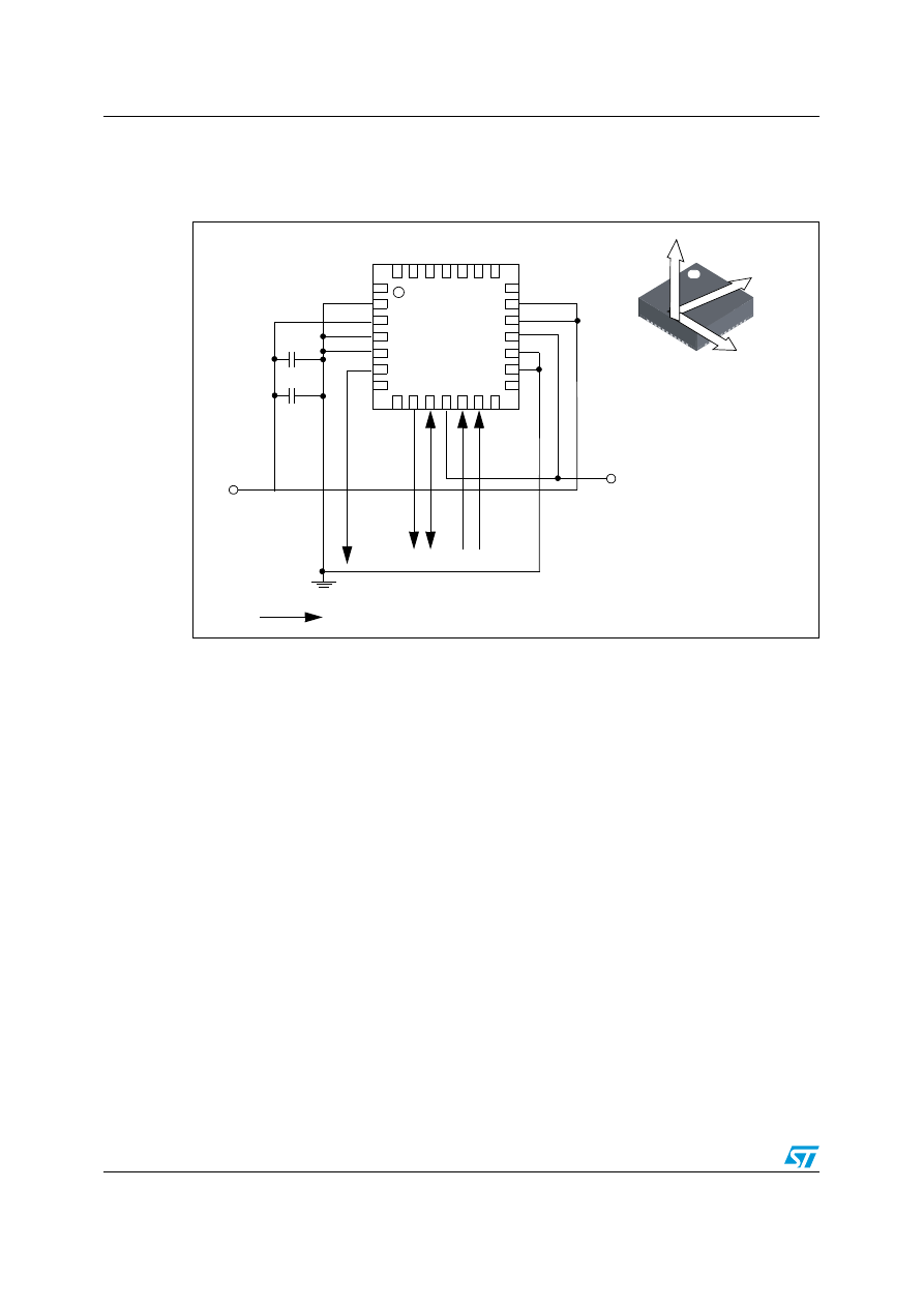
4 Application
hints
Figure 4.
AIS326DQ electrical connection
The device core is supplied through Vdd line while the I/O pads are supplied through
Vdd_IO line. Power supply decoupling capacitors (100 nF ceramic, 10 µF Al) should be
placed as near as possible to the pin 3 of the device (common design practice).
All the voltage and ground supplies must be present at the same time to have proper
behavior of the IC (refer to
). It is possible to remove Vdd maintaining Vdd_IO
without blocking the communication busses. In this condition the measurement chain is
powered off.
The functionality of the device and the measured acceleration data is selectable and
accessible through the SPI interface.
The functions, the thresholds and the timing of the interrupt pin (INT) can be completely
programmed by the user through the SPI interface.
AIS326DQ
1
7
28
22
21
15
8
14
DIRECTIONS OF THE
DETECTABLE
ACCELERATIONS
Vdd_IO
CS
SPC
SDI
/SD
O
SDO
RDY/
IN
T
10uF
Vdd
Digital signal from/to signal controller. Signal’s levels are defined by proper selection of Vdd_IO
100nF
GND
(TOP VIEW)
Y
1
X
Z
AIS326DQ
Digital interface
19/49
5 Digital
interface
The registers embedded inside the AIS326DQ may be accessed through SPI serial
interface. The latter may be SW configured to operate either in 3-wire or 4-wire interface
mode.
The embedded registers may be accessed also through an I
2
C interface. For I
2
C operation
refer to LIS3LV02DQ datasheet.
5.1 SPI
bus
interface
The AIS326DQ SPI is a bus slave. The SPI allows to write and read the registers of the
device.
The serial interface interacts with the outside world with 4 wires: CS, SPC, SDI and SDO.
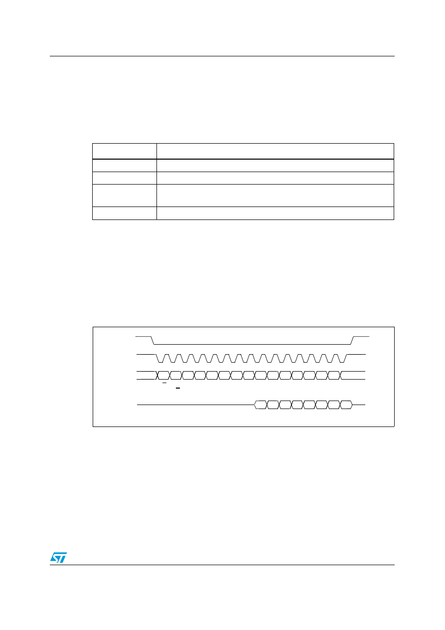
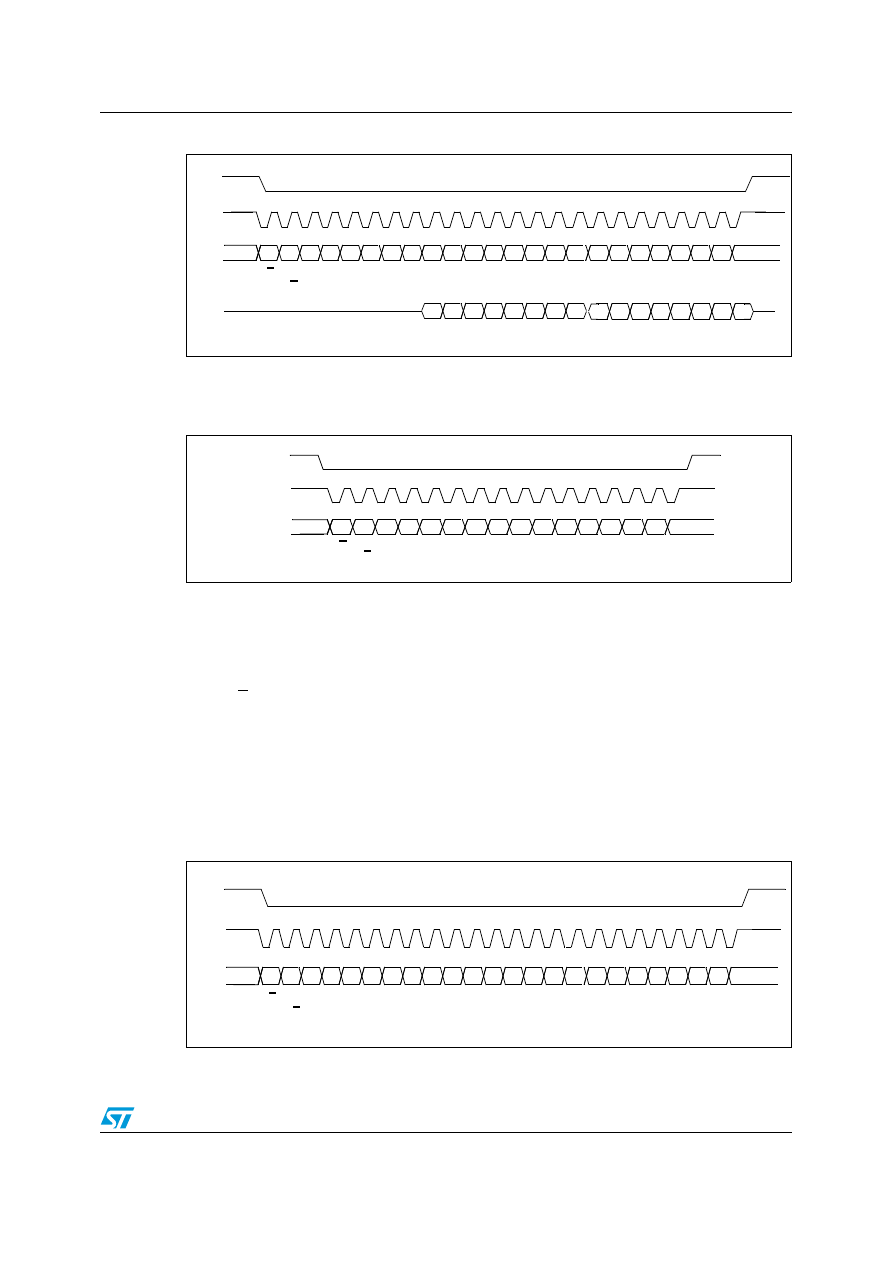
Figure 5.
Read and write protocol
CS is the serial port enable and it is controlled by the SPI master. It goes low at the start of
the transmission and goes back high at the end.
SPC is the Serial Port Clock and it is controlled by the SPI master. It is stopped high when
CS is high (no transmission).
SDI and SDO are respectively the serial port data input and output. Those lines are driven
at the falling edge of SPC and should be captured at the rising edge of SPC.
Both the read register and write register commands are completed in 16 clock pulses or in
multiple of 8 in case of multiple byte read/write. Bit duration is the time between two falling
edges of SPC. The first bit (bit 0) starts at the first falling edge of SPC after the falling edge
Table 7.
Serial interface pin description
Pin name
Pin description
CS
Chip select (logic 0: SPI enabled, logic 1: SPI disabled)
SPC
SPI serial port clock
SDI/SDO
SPI serial data input (SDI)
3-wire interface serial data output (SDO)
SDO
SPI serial data output (SDO)
CS
SPC
SDI
SDO
RW
AD5 AD4 AD3 AD2 AD1 AD0
DI7 DI6 DI5 DI4 DI3 DI2 DI1 DI0
DO7 DO6 DO5 DO4 DO3 DO2 DO1 DO0
MS
Digital interface
AIS326DQ
20/49
of CS while the last bit (bit 15, bit 23, ...) starts at the last falling edge of SPC just before the
rising edge of CS.
bit 0: RW bit. When 0, the data DI(7:0) is written into the device. When 1, the data DO(7:0)
from the device is read. In latter case, the chip will drive SDO at the start of bit 8.
bit 1: MS bit. When 0, the address will remain unchanged in multiple read/write commands.
When 1, the address will be auto increased in multiple read/write commands.
bit 2-7: address AD(5:0). This is the address field of the indexed register.
bit 8-15: data DI(7:0) (write mode). This is the data that will be written into the device (MSb
first).
bit 8-15: data DO(7:0) (read mode). This is the data that will be read from the device (MSb
first).
In multiple read/write commands further blocks of 8 clock periods will be added. When MS
bit is 0 the address used to read/write data remains the same for every block. When MS bit
is ‘1’ the address used to read/write data is increased at every block.
The function and the behavior of SDI and SDO remain unchanged.
5.1.1 SPI
Read
Figure 6.
SPI read protocol
The SPI Read command is performed with 16 clock pulses. Multiple byte read command is
performed adding blocks of 8 clock pulses at the previous one.
bit 0: READ bit. The value is 1.
bit 1: MS bit. When 0 do not increment address, when 1 increment address in multiple
reading.
bit 2-7: address AD(5:0). This is the address field of the indexed register.
bit 8-15: data DO(7:0) (read mode). This is the data that will be read from the device (MSb
first).
bit 16-... : data DO(...-8). Further data in multiple byte reading.
CS
SPC
SDI
SDO
RW
DO7 DO6 DO5 DO4 DO3 DO2 DO1 DO0
AD5 AD4 AD3 AD2 AD1 AD0
MS
AIS326DQ
Digital interface
21/49
Figure 7.
Multiple bytes SPI read protocol (2 bytes example)
5.1.2 SPI
Write
Figure 8.
SPI Write protocol
The SPI Write command is performed with 16 clock pulses. Multiple byte write command is
performed adding blocks of 8 clock pulses at the previous one.
bit 0: WRITE bit. The value is 0.
bit 1: MS bit. When 0 do not increment address, when 1 increment address in multiple
writing.
bit 2 -7: address AD(5:0). This is the address field of the indexed register.
bit 8-15: data DI(7:0) (write mode). This is the data that will be written inside the device
(MSb first).
bit 16-... : data DI(...-8). Further data in multiple byte writing.
Figure 9.
Multiple bytes SPI write protocol (2 bytes example)
CS
SPC
SDI
SDO
RW
DO7 DO6 DO5 DO4 DO3 DO2 DO1 DO0
AD5 AD4 AD3 AD2 AD1 AD0
DO15
DO14
DO13
DO12
DO11
DO10
DO9 DO8
MS
CS
SPC
SDI
RW
DI7
DI6
DI5
DI4
DI3
DI2
DI1
DI0
AD5 AD4 AD3 AD2 AD1 AD0
MS
CS
SPC
SDI
RW
AD5 AD4 AD3 AD2 AD1 AD0
DI7 DI6 DI5 DI4 DI3 DI2 DI1 DI0 DI15 DI14 DI13 DI12 DI11 DI10 DI9 DI8
MS
Digital interface
AIS326DQ
22/49
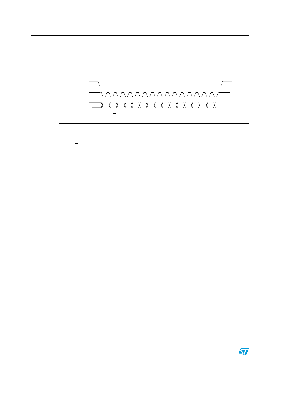
5.1.3
SPI Read in 3-wires mode
3-wires mode is entered by setting to ‘1’ bit SIM (SPI serial interface mode selection) in
CTRL_REG2.
Figure 10.
SPI read protocol in 3-wires mode
The SPI read command is performed with 16 clock pulses:
bit 0: READ bit. The value is 1.
bit 1: MS bit. When 0 do not increment address, when 1 increment address in multiple
reading.
bit 2-7: address AD(5:0). This is the address field of the indexed register.
bit 8-15: data DO(7:0) (read mode). This is the data that will be read from the device (MSb
first).
Multiple read command is also available in 3-wires mode.
CS
SPC
SDI/O
RW
DO7 DO6 DO5 DO4 DO3 DO2 DO1 DO0
AD5 AD4 AD3 AD2 AD1 AD0
MS
AIS326DQ
Register mapping
23/49
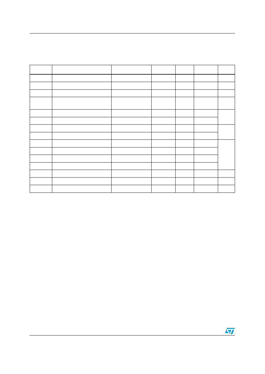
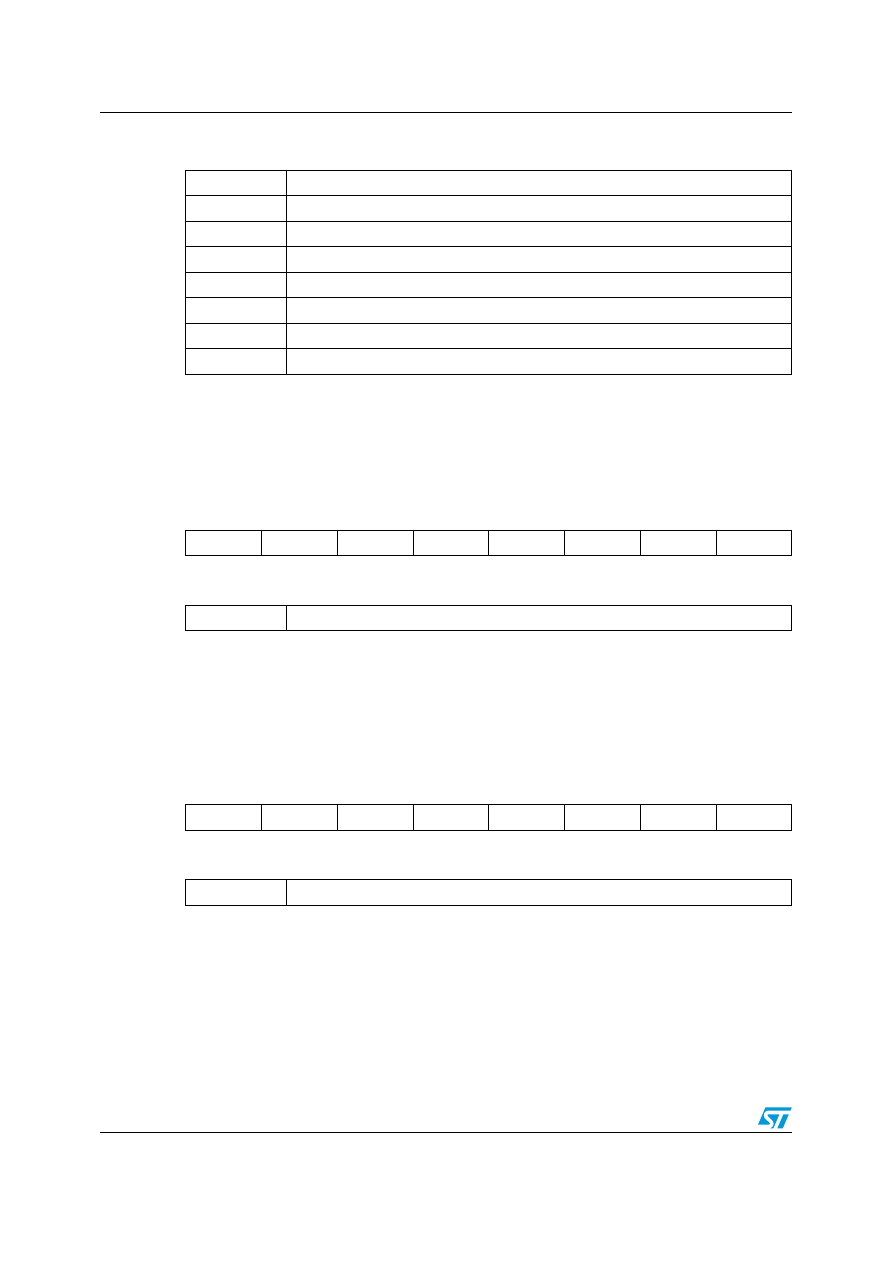
6 Register
mapping
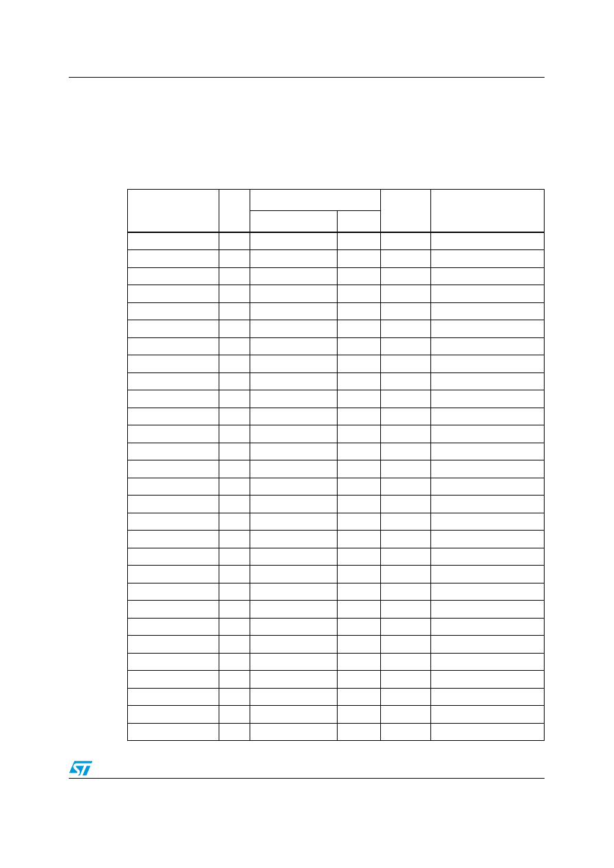
The table given below provides a listing of the 8 bit registers embedded in the device and
the related address.
Table 8.
Registers address map
Register name
Type
Register address
Default
Comment
Binary
Hex
rw
0000000 - 0001110 00 - 0E
Reserved
WHO_AM_I
r
0001111
0F
00111010
Dummy register
rw
0010000 - 0010101 10 - 15
Reserved
OFFSET_X
rw
0010110
16
Calibration Loaded at boot
OFFSET_Y
rw
0010111
17
Calibration Loaded at boot
OFFSET_Z
rw
0011000
18
Calibration Loaded at boot
GAIN_X
rw
0011001
19
Calibration Loaded at boot
GAIN_Y
rw
0011010 1A
Calibration Loaded
at
boot
GAIN_Z
rw
0011011
1B
Calibration Loaded at boot
0011100 -0011111
1C-1F
Reserved
CTRL_REG1
rw
0100000
20
00000111
CTRL_REG2
rw
0100001
21
00000000
CTRL_REG3
rw
0100010
22
00001000
HP_FILTER RESET
r
0100011
23
dummy
Dummy register
0100100-0100110
24-26
Not used
STATUS_REG
rw
0100111
27
00000000
OUTX_L
r
0101000
28
output
OUTX_H
r
0101001
29
output
OUTY_L
r
0101010
2A
output
OUTY_H
r
0101011
2B
output
OUTZ_L
r
0101100
2C
output
OUTZ_H
r
0101101
2D
output
r
0101110
2E
Reserved
0101111
2F
Not used
FF_WU_CFG
rw
0110000
30
00000000
FF_WU_SRC
rw
0110001
31
00000000
FF_WU_ACK
r
0110010
32
dummy
Dummy register
0110011
33
Not used
FF_WU_THS_L
rw
0110100
34
00000000
Register mapping
AIS326DQ
24/49
Registers marked as
Reserved must not be changed. The writing to those registers may
cause permanent damages to the device.
The content of the registers that are loaded at boot should not be changed. They contain the
factory calibration values. Their content is automatically restored when the device is
powered up.
FF_WU_THS_H
rw
0110101
35
00000000
FF_WU_DURATION rw
0110110
36
00000000
0110111
37
Not used
DD_CFG
rw
0111000
38
00000000
DD_SRC
rw
0111001
39
00000000
DD_ACK
r
0111010
3A
dummy
Dummy register
0111011
3B
Not used
DD_THSI_L
rw
0111100
3C
00000000
DD_THSI_H
rw
0111101
3D
00000000
DD_THSE_L
rw
0111110
3E
00000000
DD_THSE_H
rw
0111111
3F
00000000
1000000-1111111
40-7F
Reserved
Table 8.
Registers address map (continued)
Register name
Type
Register address
Default
Comment
Binary
Hex

AIS326DQ
Register description
25/49
7 Register
description
The device contains a set of registers which are used to control its behavior and to retrieve
acceleration data. The registers
contain the factory calibration values, it is not
necessary to change their value for normal device operation.
7.1 WHO_AM_I
(0Fh)
Addressing this register the physical address of the device is returned. For AIS326DQ the
physical address assigned in factory is 3Ah.
7.2 OFFSET_X
(16h)
7.3 OFFSET_Y
(17h)
7.4 OFFSET_Z
(18h)
Table 9.
Register
W7
W6
W5
W4
W3
W2
W1
W0
Table 10.
Register description
W7, W0
AIS326DQ physical address equal to 3Ah
Table 11.
OFFSET_X register
OX7
OX6
OX5
OX4
OX3
OX2
OX1
OX0
Table 12.
OFFSET_X register description
OX7, OX0
Digital offset trimming for X-Axis
Table 13.
OFFSET_Y register
OY7
OY6
OY5
OY4
OY3
OY2
OY1
OY0
Table 14.
OFFSET_Y register description
OY7, OY0
Digital offset trimming for Y-Axis
Table 15.
OFFSET_Z register
OZ7
OZ6
OZ5
OZ4
OZ3
OZ2
OZ1
OZ0

Register description
AIS326DQ
26/49
7.5 GAIN_X
(19h)
7.6 GAIN_Y
(1Ah)
7.7 GAIN_Z
(1Bh)
7.8 CTRL_REG1
(20h)
Table 16.
OFFSET_Z register description
OZ7, OZ0
Digital offset trimming for Z-Axis
Table 17.
GAIN_X register
GX7
GX6
GX5
GX4
GX3
GX2
GX1
GX0
Table 18.
GAIN_X register description
GX7, GX0
Digital gain trimming for X-Axis
Table 19.
GAIN_Y register
GY7
GY6
GY5
GY4
GY3
GY2
GY1
GY0
Table 20.
GAIN_Y register description
GY7, GY0
Digital gain trimming for Y-Axis
Table 21.
GAIN_Z register
GZ7
GZ6
GZ5
GZ4
GZ3
GZ2
GZ1
GZ0
Table 22.
GAIN_Z register description
GZ7, GZ0
Digital gain trimming for Z-Axis
Table 23.
CTRL_REG1 register
PD1
PD0
DF1
DF0
ST
Zen
Yen
Xen
Table 24.
CTRL_REG1 register description
PD1, PD0
Power down control
(00: power-down mode; 01, 10, 11: device on)
DF1, DF0
Decimation factor control
(00: decimate by 512; 01: decimate by 128; 10: decimate by 32; 11: decimate by 8)
AIS326DQ
Register description
27/49
PD1, PD0 bit allows to turn the device out of power-down mode. The device is in power-
down mode when PD1, PD0= “00” (default value after boot). The device is in normal mode
when either PD1 or PD0 is set to 1.
DF1, DF0 bit allows to select the data rate at which acceleration samples are produced. The
default value is “00” which corresponds to a data-rate of 40 Hz. By changing the content of
DF1, DF0 to “01”, “10” and “11” the selected data-rate will be set respectively equal to
160 Hz, 640 Hz and to 2560 Hz.
ST bit is used to activate the self test function. When the bit is set to one, an output change
will occur to the device outputs (refer to table 2 and 3 for specification) thus allowing to
check the functionality of the whole measurement chain.
Zen bit enables the Z-axis measurement channel when set to 1. The default value is 1.
Yen bit enables the Y-axis measurement channel when set to 1. The default value is 1.
Xen bit enables the X-axis measurement channel when set to 1. The default value is 1.
7.9 CTRL_REG2
(21h)
ST
Self test enable
(0: normal mode; 1: self-test active)
Zen
Z-axis enable
(0: axis off; 1: axis on)
Yen
Y-axis enable
(0: axis off; 1: axis on)
Xen
X-axis enable
(0: axis off; 1: axis on)
Table 24.
CTRL_REG1 register description (continued)
Table 25.
CTRL_REG2 register
FS
BDU
BLE
BOOT
IEN
DRDY
SIM
DAS
Table 26.
CTRL_REG2 register description
FS
Full scale selection
(0: ±2
g; 1: ±6 g)
BDU
Block data update
(0: continuous update; 1: output registers not updated between MSB and LSB
reading)
BLE
Big/little endian selection
(0: little endian; 1: big endian)
BOOT
Reboot memory content
IEN
Interrupt ENable
(0: data ready on RDY pad; 1: interrupt events on RDY pad)
DRDY
Enable data-ready generation

Register description
AIS326DQ
28/49
FS bit is used to select full scale value. After the device power-up the default full scale value
is +/-2
g. In order to obtain a +/-6 g full scale it is necessary to set FS bit to ‘1’.
BDU bit is used to inhibit output registers update between the reading of upper and lower
register parts. In default mode (BDU = ‘0’) the lower and upper register parts are updated
continuously. If it is not sure to read faster than output data rate, it is recommended to set
BDU bit to ‘1’. In this way, after the reading of the lower (upper) register part, the content of
that output registers is not updated until the upper (lower) part is read too.
This feature avoids reading LSB and MSB related to different samples.
BLE bit is used to select Big Endian or Little Endian representation for output registers. In
Big Endian’s one MSB acceleration value is located at addresses 28h (X-axis), 2Ah (Y-axis)
and 2Ch (Z-axis) while LSB acceleration value is located at addresses 29h (X-axis), 2Bh (Y-
axis) and 2Dh (Z-axis). In Little Endian representation (Default, BLE=‘0‘) the order is
inverted (refer to data register description for more details).
BOOT bit is used to refresh the content of internal registers stored in the flash memory
block. At the device power up the content of the flash memory block is transferred to the
internal registers related to trimming functions to permit a good behavior of the device itself.
If for any reason the content of trimming registers was changed it is sufficient to use this bit
to restore correct values. When BOOT bit is set to ‘1’ the content of internal flash is copied
inside corresponding internal registers and it is used to calibrate the device. These values
are factory trimmed and they are different for every accelerometer. They permit a good
behavior of the device and normally they have not to be changed. At the end of the boot
process the BOOT bit is set again to ‘0’.
IEN bit is used to switch the value present on data-ready pad between Data-Ready signal
and Interrupt signal. At power up the Data-ready signal is chosen. It is however necessary to
modify DRDY bit to enable Data-Ready signal generation.
DRDY bit is used to enable Data-Ready (RDY/INT) pin activation. If DRDY bit is ‘0’ (default
value) on Data-Ready pad a ‘0’ value is present. If a Data-Ready signal is desired it is
necessary to set to ‘1’ DRDY bit. Data-Ready signal goes to ‘1’ whenever a new data is
available for all the enabled axis. For example if Z-axis is disabled, Data-Ready signal goes
to ‘1’ when new values are available for both X and Y axis. Data-Ready signal comes back
to ‘0’ when all the registers containing values of the enabled axis are read. To be sure not to
loose any data coming from the accelerometer data registers must be read before a new
Data-Ready rising edge is generated. In this case Data-ready signal will have the same
frequency of the data rate chosen.
SIM bit selects the SPI Serial Interface Mode. When SIM is ‘0’ (default value) the 4-wire
interface mode is selected. The data coming from the device are sent to SDO pad. In 3-wire
interface mode output data are sent to SDA/SDI pad.
DAS bit permits to decide between 12 bit right justified and 16 bit left justified representation
of data coming from the device. The first case is the default case and the most significant
bits are replaced by the bit representing the sign.
SIM
SPI serial interface mode selection
(0: 4-wire interface; 1: 3-wire interface)
DAS
Data alignment selection
(0: 12 bit right justified; 1: 16 bit left justified)
Table 26.
CTRL_REG2 register description (continued)

AIS326DQ
Register description
29/49
7.10 CTRL_REG3
(22h)
FDS bit enables (FDS=1) or bypass (FDS=0) the high pass filter in the signal chain of the
sensor.
CFS1, CFS0 bits defines the coefficient Hpc to be used to calculate the -3dB cut-off
frequency of the high pass filter:
7.11 HP_FILTER_RESET
(23h)
Dummy register. Reading at this address zeroes instantaneously the content of the internal
high pass-filter. Read data is not significant.
7.12 STATUS_REG
(27h)
Table 27.
CTRL_REG3 register
ECK
HPDD
HPFF
FDS
res
res
CFS1
CFS0
Table 28.
CTRL_REG3 register description
ECK
External Clock. Default value: 0
(0: clock from internal oscillator; 1: clock from external pad)
HPDD
High Pass filter enabled for Direction Detection. Default value: 0
(0: filter bypassed; 1: filter enabled)
HPFF
High Pass filter enabled for Free-Fall and Wake-Up. Default value: 0
(0: filter bypassed; 1: filter enabled)
FDS
Filtered Data Selection. Default value: 0
(0: internal filter bypassed; 1: data from internal filter)
CFS1, CFS0
High-pass filter Cut-off Frequency Selection. Default value: 00
(00: Hpc=512
01: Hpc=1024
10: Hpc=2048
11: Hpc=4096)
f
cutoff
0.318
Hpc
---------------
ODRx
2
-----------------
⋅
=
Table 29.
STATUS_REG register
ZYXOR
ZOR
YOR
XOR
ZYXDA
ZDA
YDA
XDA
Register description
AIS326DQ
30/49
The content of this register is updated every ODR cycle, regardless of BDU bit value in
CTRL_REG2.
7.13 OUTX_L
(28h)
In big endian mode (bit BLE in CTRL_REG2 set to ‘1’) the content of this register is the MSB
acceleration data and depends on bit DAS in CTRL_REG2 register as described in the
following section.
7.14 OUTX_H
(29h)
When reading the register in “12 bit right justified” mode the most significant bits (15:12) are
replaced with bit 11 (i.e. XD15-XD12=XD11, XD11, XD11, XD11).
In big endian mode (bit BLE in CTRL_REG2 set to ‘1’) the content of this register is the LSB
acceleration data.
Table 30.
STATUS_REG register description
ZYXOR
X, Y and Z axis data overrun
ZOR
Z axis data overrun
YOR
Y axis data overrun
XOR
X axis data overrun
ZYXDA
X, Y and Z axis new data available
ZDA
Z axis new data available
YDA
Y axis new data available
XDA
X axis new data available
Table 31.
OUTX_L register
XD7
XD6
XD5
XD4
XD3
XD2
XD1
XD0
Table 32.
OUTX_L register description
XD7, XD0
X axis acceleration data LSB
Table 33.
OUTX_H register
XD15
XD14
XD13
XD12
XD11
XD10
XD9
XD8
Table 34.
OUTX_H register description
XD15, XD8
X axis acceleration data MSB

AIS326DQ
Register description
31/49
7.15 OUTY_L
(2Ah)
In big endian mode (bit BLE in CTRL_REG2 set to ‘1’) the content of this register is the MSB
acceleration data and depends on bit DAS in CTRL_REG2 register as described in the
following section.
7.16 OUTY_H
(2Bh)
When reading the register in “12 bit right justified” mode the most significant bits (15:12) are
replaced with bit 11 (i.e. YD15-YD12=YD11, YD11, YD11, YD11).
In big endian mode (bit BLE in CTRL_REG2 set to ‘1’) the content of this register is the LSB
acceleration data.
7.17 OUTZ_L
(2Ch)
In big endian mode (bit BLE in CTRL_REG2 set to ‘1’) the content of this register is the MSB
acceleration data and depends on bit DAS in CTRL_REG2 register as described in the
following section.
Table 35.
OUTY_L register
YD7
YD6
YD5
YD4
YD3
YD2
YD1
YD0
Table 36.
OUTY_L register description
YD7, YD0
Y axis acceleration data LSB
Table 37.
OUTY_H register
YD15
YD14
YD13
YD12
YD11
YD10
YD9
YD8
Table 38.
OUTY_H register description
YD15, YD8
Y axis acceleration data MSB
Table 39.
OUTZ_L register
ZD7
ZD6
ZD5
ZD4
ZD3
ZD2
ZD1
ZD0
Table 40.
OUTZ_L register description
ZD7, ZD0
Z axis acceleration data LSB

Register description
AIS326DQ
32/49
7.18 OUTZ_H
(2Dh)
When reading the register in “12 bit right justified” mode the most significant bits (15:12) are
replaced with bit 11 (i.e. ZD15-ZD12=ZD11, ZD11, ZD11, ZD11).
In big endian mode (bit BLE in CTRL_REG2 set to ‘1’) the content of this register is the LSB
acceleration data.
Table 41.
OUTZ_H register
ZD15
ZD14
ZD13
ZD12
ZD11
ZD10
ZD9
ZD8
Table 42.
OUTZ_H register description
ZD15, ZD8
Z axis acceleration data MSB

AIS326DQ
Register description
33/49
7.19 FF_WU_CFG
(30h)
Free-fall and inertial wake-up configuration register.
Table 43.
FF_WU_CFG register
AOI
LIR
ZHIE
ZLIE
YHIE
YLIE
XHIE
XLIE
Table 44.
FF_WU_CFG register description
AOI
And/Or combination of Interrupt events. Default value: 0.
(0: OR combination of interrupt events;
1: AND combination of interrupt events)
LIR
Latch interrupt request. Default value: 0.
(0: interrupt request not latched;
1: interrupt request latched)
ZHIE
Enable Interrupt request on Z High event. Default value: 0.
(0: disable interrupt request;
1: enable interrupt request on measured accel. value higher than preset threshold)
ZLIE
Enable Interrupt request on Z Low event. Default value: 0.
(0: disable interrupt request;
1: enable interrupt request on measured accel. value lower than preset threshold)
YHIE
Enable Interrupt request on Y High event. Default value: 0.
(0: disable interrupt request;
1: enable interrupt request on measured accel. value higher than preset threshold)
YLIE
Enable Interrupt request on Y Low event. Default value: 0.
(0: disable interrupt request;
1: enable interrupt request on measured accel. value lower than preset threshold)
XHIE
Enable Interrupt request on X High event. Default value: 0.
(0: disable interrupt request;
1: enable interrupt request on measured accel. value higher than preset threshold)
XLIE
Enable Interrupt request on X Low event. Default value: 0.
(0: disable interrupt request;
1: enable interrupt request on measured accel. value lower than preset threshold)
Register description
AIS326DQ
34/49
7.20 FF_WU_SRC
(31h)
7.21 FF_WU_ACK
(32h)
Dummy register. If LIR bit in FF_WU_CFG register is set to ‘1’, a reading at this address
refreshes the FF_WU_SRC register. Read data is not significant.
7.22 FF_WU_THS_L
(34h)
7.23 FF_WU_THS_H
(35h)
Table 45.
FF_WU_SRC register
X
IA
ZH
ZL
YH
YL
XH
XL
Table 46.
FF_WU_SRC register description
IA
Interrupt Active. Default value: 0
(0: no interrupt has been generated;
1: one or more interrupt events have been generated)
ZH
Z High. Default value: 0
(0: no interrupt; 1: Z High event has occurred)
ZL
Z Low. Default value: 0
(0: no interrupt; 1: Z Low event has occurred)
YH
Y High. Default value: 0
(0: no interrupt; 1: Y High event has occurred)
YL
Y Low. Default value: 0
(0: no interrupt; 1: Y Low event has occurred)
XH
X High. Default value: 0
(0: no interrupt; 1: X High event has occurred)
XL
X Low. Default value: 0
(0: no interrupt; 1: X Low event has occurred)
Table 47.
FF_WU_THS_L register
THS7
THS6
THS5
THS4
THS3
THS2
THS1
THS0
Table 48.
FF_WU_THS_L register description
THS7, THS0
Free-fall / inertial wake up acceleration threshold LSB
Table 49.
FF_WU_THS_H register
THS15
THS14
THS13
THS12
THS11
THS10
THS9
THS8
Table 50.
FF_WU_THS_H register description
THS15, THS8
Free-fall / inertial wake up acceleration threshold MSB

AIS326DQ
Register description
35/49
7.24 FF_WU_DURATION
(36h)
This register sets the minimum duration of the free-fall/wake-up event to be recognized.
7.25 DD_CFG
(38h)
Table 51.
FF_WU_DURATION register
FWD7
FWD6
FWD5
FWD4
FWD3
FWD2
FWD1
FWD0
Table 52.
FF_WU_DURATION register description
FWD7, FWD0
Minimum duration of the Free-fall/Wake-up event
Duration s
( )
FF_WU_DURATION (Dec)
ODR
------------------------------------------------------------------------
=
Table 53.
DD_CFG register
IEND
LIR
ZHIE
ZLIE
YHIE
YLIE
XHIE
XLIE
Table 54.
DD_CFG register description
IEND
Interrupt enable on direction change. Default value: 0
(0: disabled;
1: interrupt signal enabled)
LIR
Latch Interrupt request into DD_SRC reg with the DD_SRC reg cleared by reading
DD_ACK reg. Default value: 0.
(0: interrupt request not latched;
1: interrupt request latched)
ZHIE
Enable interrupt generation on Z high event. Default value: 0
(0: disable interrupt request;
1: enable interrupt request on measured accel. value higher than preset threshold)
ZLIE
Enable interrupt generation on Z low event. Default value: 0
(0: disable interrupt request;
1: enable interrupt request on measured accel. value lower than preset threshold)
YHIE
Enable interrupt generation on Y high event. Default value: 0
(0: disable interrupt request;
1: enable interrupt request on measured accel. value higher than preset threshold)
YLIE
Enable interrupt generation on Y low event. Default value: 0
(0: disable interrupt request;
1: enable interrupt request on measured accel. value lower than preset threshold)

Register description
AIS326DQ
36/49
Direction-detector configuration register.
7.26 DD_SRC
(39h)
Direction detector source register.
XHIE
Enable interrupt generation on X high event. Default value: 0
(0: disable interrupt request;
1: enable interrupt request on measured accel. value higher than preset threshold)
XLIE
Enable interrupt generation on X low event. Default value: 0
(0: disable interrupt request;
1: enable interrupt request on measured accel. value lower than preset threshold)
Table 54.
DD_CFG register description (continued)
Table 55.
DD_SRC register
X
IA
ZH
ZL
YH
YL
XH
XL
Table 56.
DD_SRC register description
IA
Interrupt event from direction change.
(0: no direction changes detected;
1: direction has changed from previous measurement)
ZH
Z High. Default value: 0
(0: Z below THSI threshold;
1: Z accel. exceeding THSE threshold along positive direction of acceleration axis)
ZL
Z Low. Default value: 0
(0: Z below THSI threshold;
1: Z accel. exceeding THSE threshold along negative direction of acceleration axis)
YH
Y High. Default value: 0
(0: Y below THSI threshold;
1: Y accel. exceeding THSE threshold along positive direction of acceleration axis)
YL
Y Low. Default value: 0
(0: Y below THSI threshold;
1: Y accel. exceeding THSE threshold along negative direction of acceleration axis)
XH
X High. Default value: 0
(0: X below THSI threshold;
1: X accel. exceeding THSE threshold along positive direction of acceleration axis)
XL
X Low. Default value: 0
(0: X below THSI threshold;
1: X accel. exceeding THSE threshold along negative direction of acceleration axis)
AIS326DQ
Register description
37/49
7.27 DD_ACK
(3Ah)
Dummy register. If LIR bit in DD_CFG register is set to ‘1’, a reading at this address
refreshes the DD_SRC register. Read data is not significant.
7.28 DD_THSI_L
(3Ch)
7.29 DD_THSI_H
(3Dh)
7.30 DD_THSE_L
(3Eh)
7.31 DD_THSE_H
(3Fh)
Table 57.
DD_THSI_L register
THSI7
THSI6
THSI5
THSI4
THSI3
THSI2
THSI1
THSI0
Table 58.
DD_THSI_L register description
THSI7, THSI0
Direction detection internal threshold LSB
Table 59.
DD_THSI_H register
THSI15
THSI14
THSI13
THSI12
THSI11
THSI10
THSI9
THSI8
Table 60.
DD_THSI_H register description
THSI15, THSI8
Direction detection internal threshold MSB
Table 61.
DD_THSE_L register
THSE7
THSE6
THSE5
THSE4
THSE3
THSE2
THSE1
THSE0
Table 62.
DD_THSE_L register description
THSE7, THSE0
Direction detection external threshold LSB
Table 63.
DD_THSE_H register
THSE15
THSE14
THSE13
THSE12
THSE11
THSE10
THSE9
THSE8
Table 64.
DD_THSE_H register description
THSE15, THSE8
Direction detection external threshold MSB
Typical performance characteristics
AIS326DQ
38/49
8
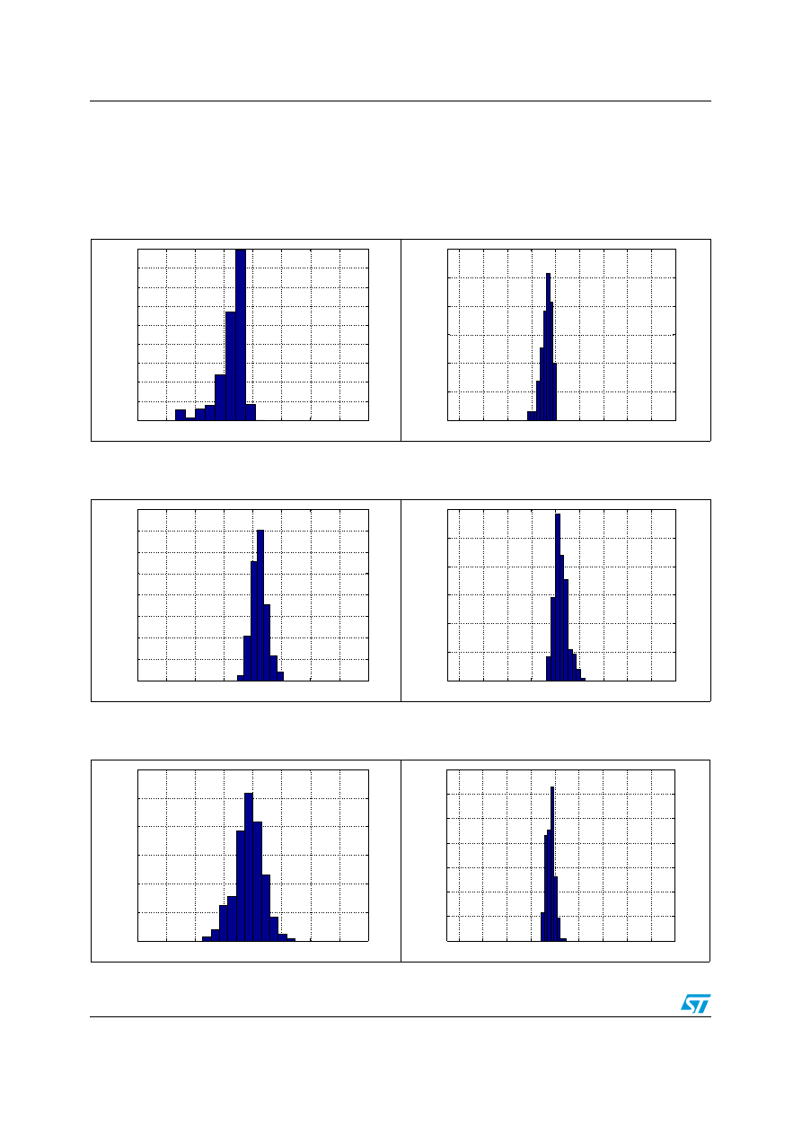
Typical performance characteristics
8.1
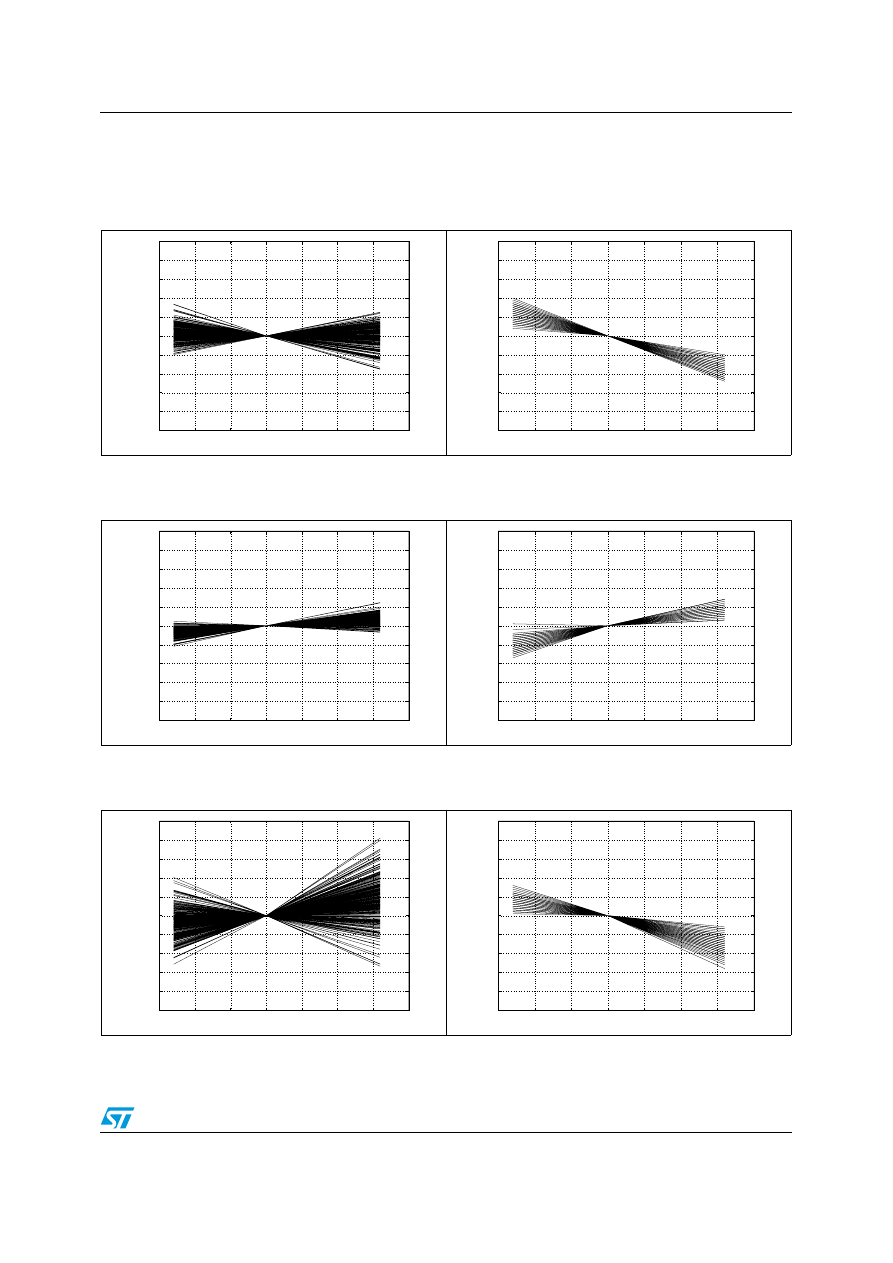
Mechanical characteristics at 25 °C
Figure 11.
X-axis zero-
g level at 3.3 V
Figure 12.
X-axis sensitivity at 3.3 V
Figure 13.
Y-axis zero-
g level at 3.3 V
Figure 14.
Y-axis sensitivity at 3.3 V
Figure 15.
Z-axis zero-
g level at 3.3 V
Figure 16.
Z-axis sensitivity at 3.3 V
−80
−60
−40
−20
0
20
40
60
80
0
5
10
15
20
25
30
35
40
45
Zero−g Level Offset [mg]
Percent of parts [%]
940
960
980
1000
1020
1040
1060
1080
1100
1120
0
5
10
15
20
25
30
Sensitivity [LSB/g]
Percent of parts [%]
−80
−60
−40
−20
0
20
40
60
80
0
5
10
15
20
25
30
35
40
Zero−g Level Offset [mg]
Percent of parts [%]
940
960
980
1000
1020
1040
1060
1080
1100
1120
0
5
10
15
20
25
30
Sensitivity [LSB/g]
Percent of parts [%]
−80
−60
−40
−20
0
20
40
60
80
0
5
10
15
20
25
30
Zero−g Level Offset [mg]
Percent of parts [%]
940
960
980
1000
1020
1040
1060
1080
1100
1120
0
5
10
15
20
25
30
35
Sensitivity [LSB/g]
Percent of parts [%]
AIS326DQ
Typical performance characteristics
39/49
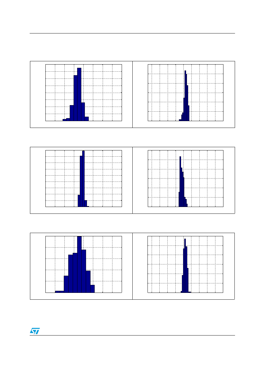
8.2
Mechanical characteristics at -40 °C
Figure 17.
X-axis zero-g level at 3.3 V
Figure 18.
X-axis sensitivity at 3.3 V
Figure 19.
Y-axis zero-
g level at 3.3 V
Figure 20.
Y-axis sensitivity at 3.3 V
Figure 21.
Z-axis zero-
g level at 3.3 V
Figure 22.
Z-axis sensitivity at 3.3 V
−80
−60
−40
−20
0
20
40
60
80
0
5
10
15
20
25
30
35
40
Zero−g Level Offset [mg]
Percent of parts [%]
940
960
980
1000
1020
1040
1060
1080
1100
1120
0
5
10
15
20
25
30
Sensitivity [LSB/g]
Percent of parts [%]
−80
−60
−40
−20
0
20
40
60
80
0
5
10
15
20
25
30
35
40
45
Zero−g Level Offset [mg]
Percent of parts [%]
940
960
980
1000
1020
1040
1060
1080
1100
1120
0
5
10
15
20
25
30
Sensitivity [LSB/g]
Percent of parts [%]
−80
−60
−40
−20
0
20
40
60
80
0
5
10
15
20
25
Zero−g Level Offset [mg]
Percent of parts [%]
940
960
980
1000
1020
1040
1060
1080
1100
1120
0
5
10
15
20
25
30
Sensitivity [LSB/g]
Percent of parts [%]
Typical performance characteristics
AIS326DQ
40/49
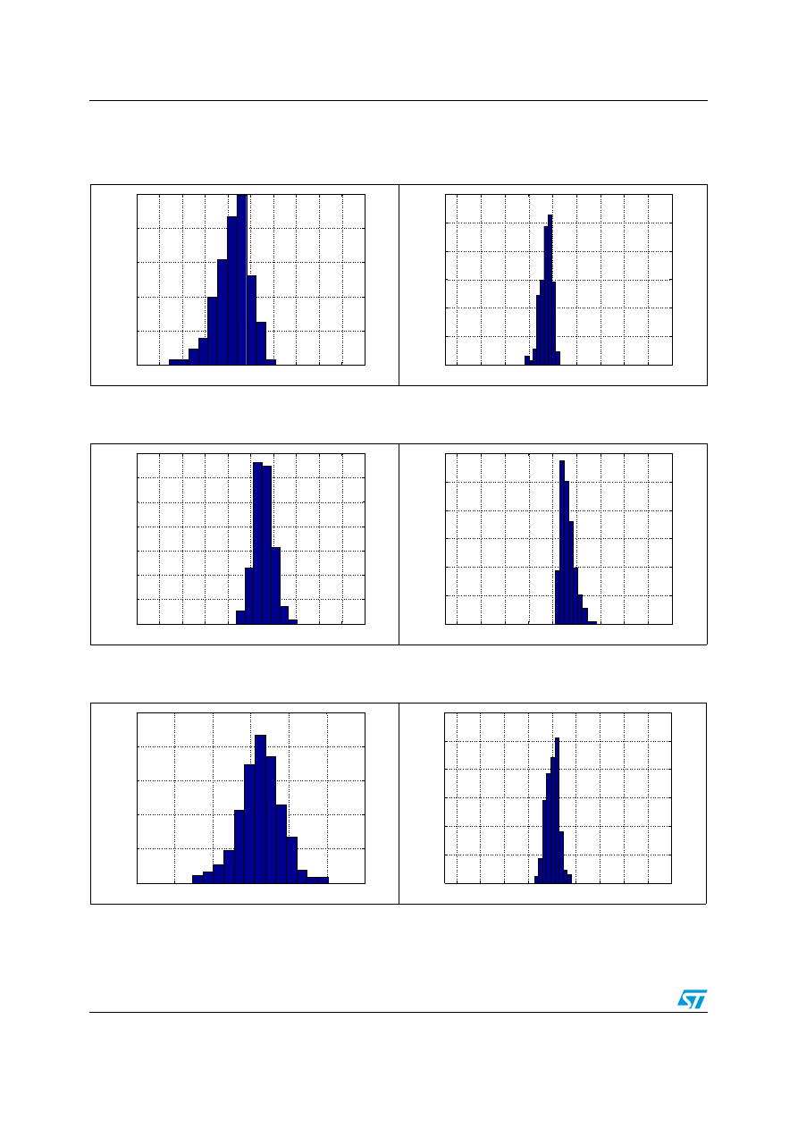
8.3
Mechanical characteristics at 105 °C
Figure 23.
X-axis zero-
g level at 3.3 V
Figure 24.
X-axis sensitivity at 3.3 V
Figure 25.
Y-axis zero-
g level at 3.3 V
Figure 26.
Y-axis sensitivity at 3.3 V
Figure 27.
Z-axis zero-
g level at 3.3 V
Figure 28.
Z-axis sensitivity at 3.3 V
−100
−80
−60
−40
−20
0
20
40
60
80
100
0
5
10
15
20
25
Zero−g Level Offset [mg]
Percent of parts [%]
920
940
960
980
1000
1020
1040
1060
1080
1100
0
5
10
15
20
25
30
Sensitivity [LSB/g]
Percent of parts [%]
−100
−80
−60
−40
−20
0
20
40
60
80
100
0
5
10
15
20
25
30
35
Zero−g Level Offset [mg]
Percent of parts [%]
940
960
980
1000
1020
1040
1060
1080
1100
1120
0
5
10
15
20
25
30
Sensitivity [LSB/g]
Percent of parts [%]
−150
−100
−50
0
50
100
150
0
5
10
15
20
25
Zero−g Level Offset [mg]
Percent of parts [%]
920
940
960
980
1000
1020
1040
1060
1080
1100
0
5
10
15
20
25
30
Sensitivity [LSB/g]
Percent of parts [%]
AIS326DQ
Typical performance characteristics
41/49
8.4 Mechanical
characteristics
derived from measurement in the
-40 °C to +105 °C temperature range
Figure 29.
X-axis zero-
g level change vs.
temperature at 3.3 V
Figure 30.
X-axis sensitivity change vs.
temperature at 3.3 V
Figure 31.
Y-axis zero-
g level change vs.
temperature at 3.3 V
Figure 32.
Y-axis sensitivity change vs.
temperature at 3.3 V
Figure 33.
Z-axis zero-
g level change vs.
temperature at 3.3 V
Figure 34.
Z-axis sensitivity change vs.
temperature at 3.3 V
−50
−25
0
25
50
75
100
125
−100
−80
−60
−40
−20
0
20
40
60
80
100
Temp [
o
C]
Zero−g Level [mg]
−50
−25
0
25
50
75
100
125
−5
−4
−3
−2
−1
0
1
2
3
4
5
Temp [
o
C]
Sensitivity [%]
−50
−25
0
25
50
75
100
125
−100
−80
−60
−40
−20
0
20
40
60
80
100
Temp [
o
C]
Zero−g Level [mg]
−50
−25
0
25
50
75
100
125
−5
−4
−3
−2
−1
0
1
2
3
4
5
Temp [
o
C]
Sensitivity [%]
−50
−25
0
25
50
75
100
125
−100
−80
−60
−40
−20
0
20
40
60
80
100
Temp [
o
C]
Zero−g Level [mg]
−50
−25
0
25
50
75
100
125
−5
−4
−3
−2
−1
0
1
2
3
4
5
Temp [
o
C]
Sensitivity [%]
Typical performance characteristics
AIS326DQ
42/49
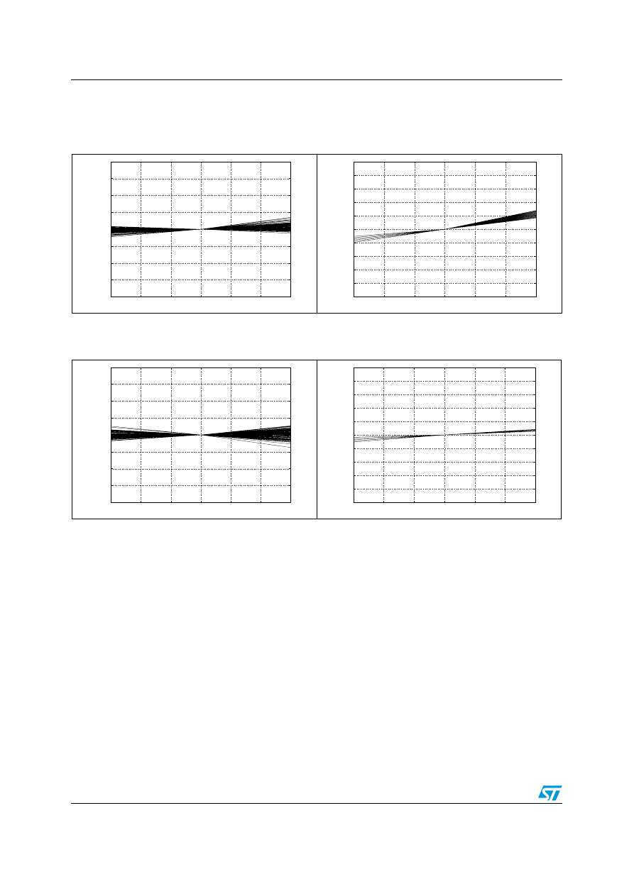
8.5 Electro-mechanical
characteristics at 25 °C
Figure 35.
X and Y axes zero-
g level as
function of supply voltage
Figure 36.
X and Y axes sensitivity as function
of supply voltage
Figure 37.
Z axis zero-
g level as function of
supply voltage
Figure 38.
Z axis sensitivity as function of
supply voltage
3
3.1
3.2
3.3
3.4
3.5
3.6
−80
−60
−40
−20
0
20
40
60
80
Vdd [V]
Normalized Zero−g Level [mg]
3
3.1
3.2
3.3
3.4
3.5
3.6
−5
−4
−3
−2
−1
0
1
2
3
4
5
Vdd [V]
Normalized Sensitivity [%]
3
3.1
3.2
3.3
3.4
3.5
3.6
−80
−60
−40
−20
0
20
40
60
80
Vdd [V]
Normalized Zero−g Level [mg]
3
3.1
3.2
3.3
3.4
3.5
3.6
−5
−4
−3
−2
−1
0
1
2
3
4
5
Vdd [V]
Normalized Sensitivity [%]
AIS326DQ
Typical performance characteristics
43/49
8.6
Electrical characteristics at 25 °C
8.7 Electrical
characteristics at -40 °C
8.8 Electrical
characteristics at 105 °C
Figure 39.
Current consumption in power-
down mode (Vdd=3.3 V)
Figure 40.
Current consumption in operational
mode (Vdd=3.3 V)
Figure 41.
Current consumption in power-
down mode (Vdd=3.3 V)
Figure 42.
Current consumption in operational
mode (Vdd=3.3 V)
Figure 43.
Current consumption in power-
down mode (Vdd=3.3 V)
Figure 44.
Current consumption in operational
mode (Vdd=3.3 V)
−2
−1
0
1
2
3
4
5
6
7
0
5
10
15
20
25
Current consumption [uA]
Percent of parts [%]
500
550
600
650
700
750
800
850
0
5
10
15
20
25
Current consumption [uA]
Percent of parts [%]
−2
−1
0
1
2
3
4
5
6
7
0
5
10
15
20
25
30
Current consumption [uA]
Percent of parts [%]
500
550
600
650
700
750
800
850
0
5
10
15
20
25
Current consumption [uA]
Percent of parts [%]
−2
−1
0
1
2
3
4
5
6
7
0
5
10
15
20
25
30
Current consumption [uA]
Percent of parts [%]
500
550
600
650
700
750
800
850
0
5
10
15
20
25
30
35
Current consumption [uA]
Percent of parts [%]

Soldering information
AIS326DQ
44/49
9 Soldering
information
The QFPN-28 package is compliant with the ECOPACK
®
, RoHS and “Green” standard.
It is qualified for soldering heat resistance according to JEDEC J-STD-020C, in MSL3
condition.
Land pattern and soldering recommendations are also available at
www.st.com/
.
9.1 General
guidelines
about soldering surface mount
accelerometer
As common PCB design and industrial practice when considering accelerometer soldering,
there are always 3 elements to take into consideration:
1.
PCB with its own conductive layers (i.e. copper) and other organic materials used for
board protection and dielectric isolation.
2.
ACCELEROMETER to be mounted on the board. Accelerometer senses acceleration,
but it senses also the mechanical stress coming from the board. This stress is
minimized with simple PCB design rules.
3.
SOLDERING PASTE like SnAgCu. This soldering paste can be dispensed on the board
with a screen printing method through a stencil. The pattern of the soldering paste on
the PCB is given by the stencil mask itself.
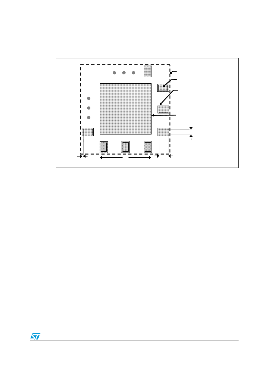
9.2 PCB
design
guidelines
PCB land and solder masking general recommendations are shown in
. Refer to
for specific device size, land count and pitch.
●
It is recommended to open solder mask external to PCB land;
●
It is mandatory, for correct device functionality, that some clearance is ensured to be
present between accelerometer thermal pad and PCB. In order to obtain this clearance
it is recommended to open the PCB thermal pad solder mask;
●
The area below the sensor (on the same side of the board) must be defined as keep-
out area. It is strongly recommended not to place any structure in top metal layer
underneath the sensor;
●
Traces connected to pads should be as much symmetric as possible. Symmetry and
balance for pad connection will help component self alignment and will lead to a better
control of solder paste reduction after reflow;
●
For better performances over temperature it is strongly recommended not to place
large insertion components like buttons or shielding boxes at distance less than 2 mm
from the sensor;
●
Central die pad and “Pin 1 Indicator” are physically connected to GND. Leave “Pin 1
Indicator” unconnected during soldering.
AIS326DQ
Soldering information
45/49
9.2.1
PCB design rules
Figure 45.
Recommended land and solder mask design for QFPN packages
A = Clearance from PCB land edge to solder mask opening
≤ 0.1 mm to ensure that some
solder mask remains between PCB pads
B = PCB land length = QFPN solder pad length + 0.1 mm
C = PCB land width = QFPN solder pad width + 0.1 mm
D = PCB thermal pad solder mask opening = QFPN thermal pad side + 0.2 mm
9.3
Stencil design and solder paste application
The thickness and the pattern of the soldering paste are important for the proper
accelerometer mounting process.
●
Stainless steel stencils are recommended for solder paste application
●
A stencil thickness of 125 - 150 µm (5 - 6 mils) is recommended for screen printing
●
The final thickness of soldering paste should allow proper cleaning of flux residuals and
clearance between sensor package and PCB
●
Stencil aperture should have rectangular shape with dimension up to 25 µm (1mil)
smaller than PCB land
●
The openings of the stencil for the signal pads should be between 50% and 80% of the
PCB pad area
●
Optionally, for better solder paste release, the aperture walls should be trapezoidal and
the corners rounded
●
The fine pitch of the IC leads requires accurate alignment of the stencil to the printed
circuit board. The stencil and printed circuit assembly should be aligned to within 25 µm
(1 mil) prior to application of the solder paste.
PACKAGE FOOTPRINT
PCB LAND
SOLDER MASK OPENING
PCB THERMAL PAD NOT TO
BE DESIGNED ON PCB
PCB THERMAL PAD SOLDER
MASK OPENING SUGGESTED
TO INCREASE DEVICE
THERMAL PAD TO PCB
CLEARANCE
A
B
C
D

Soldering information
AIS326DQ
46/49
9.4 Process
consideration
●
In case of use of no self-cleaning solder paste it is mandatory proper washing of the
board after soldering to eliminate any possible source of leakage between adjacent
pads due to flux residues
●
The PCB soldering profile depends on the number, size and placement of components
in the application board. It is not functional to define a specific soldering profile for the
accelerometer only. Customer should use a time and temperature reflow profile that is
derived from the PCB design and manufacturing experience.
AIS326DQ
Package information
47/49
10 Package
information
In order to meet environmental requirements, ST offers these devices in ECOPACK
®
packages. These packages have a lead-free second level interconnect. The category of
second Level Interconnect is marked on the package and on the inner box label, in
compliance with JEDEC Standard JESD97. The maximum ratings related to soldering
conditions are also marked on the inner box label. ECOPACK
®
is an ST trademark.
ECOPACK
®
specifications are available at:
www.st.com
.
Figure 46.
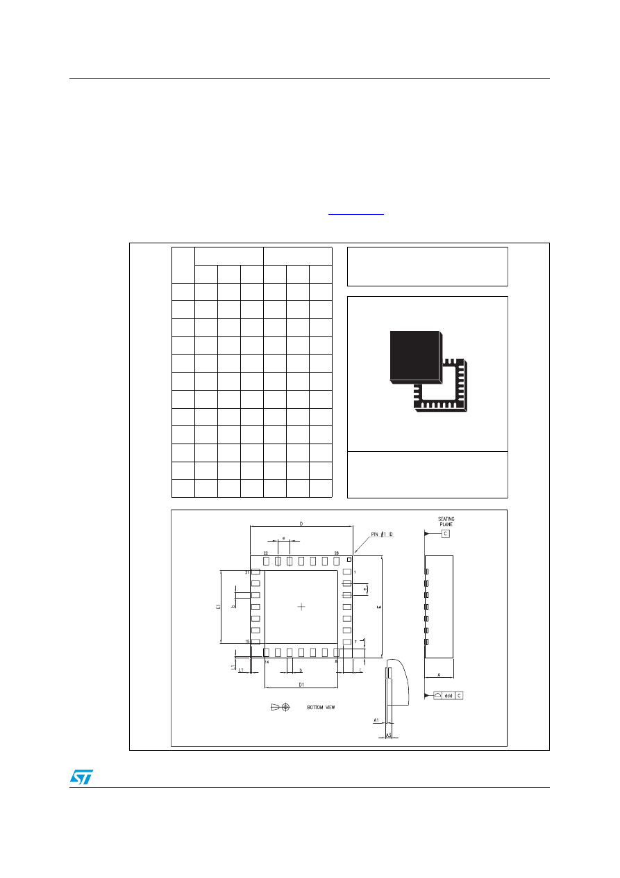
QFPN-28 mechanical data and package dimensions
OUTLINE AND
MECHANICAL DATA
DIM.
mm
inch
MIN.
TYP.
MAX.
MIN.
TYP.
MAX.
A
1.70
1.80
1.90
0.067
0.071
0.075
A1
0.05
0.002
A3
0.203
0.008
b
0.30
0.35
0.40
0.012
0.014
0.016
D
6.85
7.0
7.15
0.270
0.275
0.281
D1
4.90
5.00
5.10
0.192
0.197
0.20
E
6.85
7.0
7.15
0.270
0.275
0.281
E1
4.90
5.00
5.10
0.192
0.197
0.20
e
0.80
0.0315
L
0.45
0.55
0.65
0.018
0..022
0.025
L1
0.10
0.004
ddd
0.08
0.003
QFPN-28 (7x7x1.8mm)
Quad Flat Package No lead
7787120 C

Revision history
AIS326DQ
48/49
Table 65.
Document revision history
Date
Revision
Changes
20-Aug-2008
1
Initial release.

AIS326DQ
49/49
Please Read Carefully:
Information in this document is provided solely in connection with ST products. STMicroelectronics NV and its subsidiaries (“ST”) reserve the
right to make changes, corrections, modifications or improvements, to this document, and the products and services described herein at any
time, without notice.
All ST products are sold pursuant to ST’s terms and conditions of sale.
Purchasers are solely responsible for the choice, selection and use of the ST products and services described herein, and ST assumes no
liability whatsoever relating to the choice, selection or use of the ST products and services described herein.
No license, express or implied, by estoppel or otherwise, to any intellectual property rights is granted under this document. If any part of this
document refers to any third party products or services it shall not be deemed a license grant by ST for the use of such third party products
or services, or any intellectual property contained therein or considered as a warranty covering the use in any manner whatsoever of such
third party products or services or any intellectual property contained therein.
UNLESS OTHERWISE SET FORTH IN ST’S TERMS AND CONDITIONS OF SALE ST DISCLAIMS ANY EXPRESS OR IMPLIED
WARRANTY WITH RESPECT TO THE USE AND/OR SALE OF ST PRODUCTS INCLUDING WITHOUT LIMITATION IMPLIED
WARRANTIES OF MERCHANTABILITY, FITNESS FOR A PARTICULAR PURPOSE (AND THEIR EQUIVALENTS UNDER THE LAWS
OF ANY JURISDICTION), OR INFRINGEMENT OF ANY PATENT, COPYRIGHT OR OTHER INTELLECTUAL PROPERTY RIGHT.
UNLESS EXPRESSLY APPROVED IN WRITING BY AN AUTHORIZED ST REPRESENTATIVE, ST PRODUCTS ARE NOT
RECOMMENDED, AUTHORIZED OR WARRANTED FOR USE IN MILITARY, AIR CRAFT, SPACE, LIFE SAVING, OR LIFE SUSTAINING
APPLICATIONS, NOR IN PRODUCTS OR SYSTEMS WHERE FAILURE OR MALFUNCTION MAY RESULT IN PERSONAL INJURY,
DEATH, OR SEVERE PROPERTY OR ENVIRONMENTAL DAMAGE. ST PRODUCTS WHICH ARE NOT SPECIFIED AS "AUTOMOTIVE
GRADE" MAY ONLY BE USED IN AUTOMOTIVE APPLICATIONS AT USER’S OWN RISK.
Resale of ST products with provisions different from the statements and/or technical features set forth in this document shall immediately void
any warranty granted by ST for the ST product or service described herein and shall not create or extend in any manner whatsoever, any
liability of ST.
ST and the ST logo are trademarks or registered trademarks of ST in various countries.
Information in this document supersedes and replaces all information previously supplied.
The ST logo is a registered trademark of STMicroelectronics. All other names are the property of their respective owners.
© 2008 STMicroelectronics - All rights reserved
STMicroelectronics group of companies
Australia - Belgium - Brazil - Canada - China - Czech Republic - Finland - France - Germany - Hong Kong - India - Israel - Italy - Japan -
Malaysia - Malta - Morocco - Singapore - Spain - Sweden - Switzerland - United Kingdom - United States of America
www.st.com
Document Outline
- 1 Block diagram and pin description
- 2 Mechanical and electrical specifications
- 3 Functionality
- 4 Application hints
- 5 Digital interface
- 6 Register mapping
- 7 Register description
- 7.1 WHO_AM_I (0Fh)
- 7.2 OFFSET_X (16h)
- 7.3 OFFSET_Y (17h)
- 7.4 OFFSET_Z (18h)
- 7.5 GAIN_X (19h)
- 7.6 GAIN_Y (1Ah)
- 7.7 GAIN_Z (1Bh)
- 7.8 CTRL_REG1 (20h)
- 7.9 CTRL_REG2 (21h)
- 7.10 CTRL_REG3 (22h)
- 7.11 HP_FILTER_RESET (23h)
- 7.12 STATUS_REG (27h)
- 7.13 OUTX_L (28h)
- 7.14 OUTX_H (29h)
- 7.15 OUTY_L (2Ah)
- 7.16 OUTY_H (2Bh)
- 7.17 OUTZ_L (2Ch)
- 7.18 OUTZ_H (2Dh)
- 7.19 FF_WU_CFG (30h)
- 7.20 FF_WU_SRC (31h)
- 7.21 FF_WU_ACK (32h)
- 7.22 FF_WU_THS_L (34h)
- 7.23 FF_WU_THS_H (35h)
- 7.24 FF_WU_DURATION (36h)
- 7.25 DD_CFG (38h)
- 7.26 DD_SRC (39h)
- 7.27 DD_ACK (3Ah)
- 7.28 DD_THSI_L (3Ch)
- 7.29 DD_THSI_H (3Dh)
- 7.30 DD_THSE_L (3Eh)
- 7.31 DD_THSE_H (3Fh)
- 8 Typical performance characteristics
- 8.1 Mechanical characteristics at 25 ˚C
- 8.2 Mechanical characteristics at -40 ˚C
- 8.3 Mechanical characteristics at 105 ˚C
- 8.4 Mechanical characteristics derived from measurement in the -40 ˚C to +105 ˚C temperature range
- Figure 29. X-axis zero-g level change vs. temperature at 3.3 V
- Figure 30. X-axis sensitivity change vs. temperature at 3.3 V
- Figure 31. Y-axis zero-g level change vs. temperature at 3.3 V
- Figure 32. Y-axis sensitivity change vs. temperature at 3.3 V
- Figure 33. Z-axis zero-g level change vs. temperature at 3.3 V
- Figure 34. Z-axis sensitivity change vs. temperature at 3.3 V
- 8.5 Electro-mechanical characteristics at 25 ˚C
- 8.6 Electrical characteristics at 25 ˚C
- 8.7 Electrical characteristics at -40 ˚C
- 8.8 Electrical characteristics at 105 ˚C
- 9 Soldering information
- 10 Package information
- 11 Revision history
Wyszukiwarka
Podobne podstrony:
3axis Digital Accelerometer ADXL345
Legislacja ST cz 1 id 264961 Nieznany
Oglaszanie ST cz 2 id 333651 Nieznany
cw2 st dys 2 id 123175 Nieznany
analiza paliw st decrypted id Nieznany (2)
Projekt ST przenosnik1 id 39959 Nieznany
Legislacja adm ST cz 3 id 264 Nieznany
8 psyg,st www id 47071 Nieznany (2)
cw2 st dys id 123174 Nieznany
pkt 06 ST id 360232 Nieznany
DIGITAL OUTPUT ANGULAR ACCELEROMETER 8556
kn gik inz st 5 5 id 236836 Nieznany
accelerometer f c id 50630 Nieznany (2)
badanie kardio i pulmo st id 77 Nieznany (2)
więcej podobnych podstron