
International Workshop on ADC Modelling (IMEKO), May 7-9, 1996, Smolenice Castle, Slovak Republic
___________________________________________________________________________________________________
Page 1
APPLICATIONS OF POLYPHASE FILTERS FOR BANDPASS
SIGMA-DELTA ANALOG-TO-DIGITAL CONVERSION
Artur Krukowski, Izzet Kale and Richard C. S. Morling
University of Westminster
School of Electronic and Manufacturing System Engineering
115 New Cavendish Street, London W1M 8JS, UK
email: artur@cmsa.westminster.ac.uk
Abstract
The traditional lowpass Sigma-Delta (
Σ∆)
based Analog-to-Digital (A/D) conversion
principle has been recently extended to bandpass for direct IF conversion. Such converter
offers high Signal-to-Noise (SNR) ratios for narrowband signals relative to the sampling
frequency, at significantly lower oversampling ratios in comparison to the conventional
lowpass
Σ∆
converters. In this paper a sixth-order modulator sampled at 1.82MHz coupled
with a multistage polyphase decimation filter is reported for the conversion of bandpass signals
centred at 455kHz with 14kHz bandwidth. The decimation filter is using a small number of
short-wordlength filter coefficients. The simulations undertaken demonstrated that this setup
realises 124.3dB SNR with less than 4
µ
dB passband ripples for a half/full-scale composite
20-sinewave input signal potential of up to 20-bit performance. The resultant converter can
directly accomplish demodulation of narrow-band AM signals.
Introduction
Σ∆
modulation is a technique employed in A/D conversion which makes use of
oversampling and digital signal processing in order to achieve a high level of accuracy.
Σ∆
modulators are designed such that the noise is shaped away from the band of interest, thus
retaining the original signal in the noise-free band. This noise can be then filtered by utilising an
appropriate digital decimation filter. Such a decimation filter is composed of a high quality
bandpass filter and a sampling rate converter which brings the sampling frequency down to the
required one for a given application. For example for audio applications the sampling rate is
decreased down to the audio signal Nyquist frequency. In other applications, like in the front-
end of a radio receiver, bandpass converter [1]-[2] is used to perform the direct conversion to
digital at either intermediate- or radio-frequency.
Filters used in the decimation filter must perform both filtering of the out of band
quantization noise and prevent excess aliasing introduced during sampling rate decreasing.
They must also be very efficient computationally as the filtering is usually performed at a high
rate. Additionally, for precision conversion of wide-band signals they must also have very small
passband ripples, less than half the quantization step for the given resolution. Here polyphase
structures come very handy. They can achieve lowpass filtering with very small passband
ripples, very high stopband attenuation for a very small computation burden. Their application
for audio band lowpass
Σ∆
conversion has already been reported in several publications [3]. In
this paper we will show that they are also very attractive and viable for bandpass
Σ∆
conversion decimation filters.
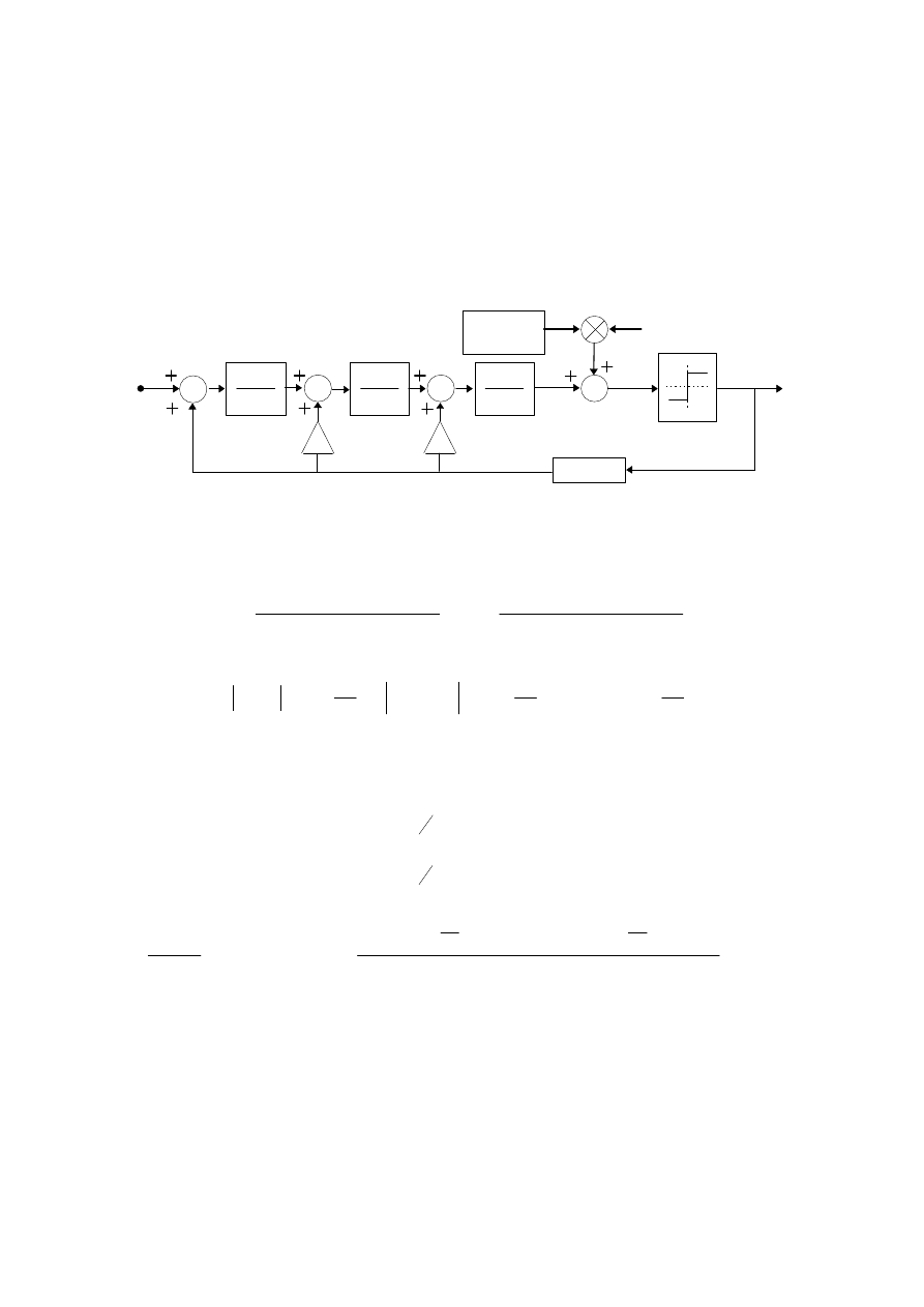
Sigma-Delta Modulator Design
The typical way of designing a bandpass modulator is to use an existing high-quality
lowpass SD modulator and perform a z
z
→
-
2
frequency transformation on the feedback loop
International Workshop on ADC Modelling (IMEKO), May 7-9, 1996, Smolenice Castle, Slovak Republic
___________________________________________________________________________________________________
Page 2
filter transfer function. If in the prototype modulator the loop filter is a cascade of three first-
order integrators (L=3), after transformation we get a modulator (Figure 1) with a cascade of
three second-order notches located at half Nyquist (quarter of the sampling frequency). The
equation describing the modulator behaviour is given in (1). Even if the resulting noise shaping
transfer function and therefore the noise power spectrum (2) are dependent on modulator
coefficient values, for R>8 the noise transfer function can be approximated with (1+z
-2
)
3
. The
theoretical shape of the quantization noise for a three-loop modulator used in our converter
design is given in (2) and presented in Figure 2 for half full-scale composite 20-tone signal.
Z
2
z
2
+1
Σ
Σ
3
9
Σ
1-bit D/A
-1
1
Quantiser
Input
Output
0.7
Σ
White Noise
(Dither)
Z
2
z
2
+1
1
z
2
+1
Figure 1: The bandpass
Σ∆
modulator converted from the lowpass version via z=-z
2
transformation.
( )
( )
(
)
( )
Y z
z
z
z
z
X z
z
z
z
z
E z
=
−
−
−
+
+
−
−
−
−
−
−
−
−
−
−
−
2
2
4
6
2
3
2
4
6
1 10
18
8
1
1 10
18
8
(1)
( )
( )
[
]
(
)
(
)
S
f
H
z
S
f
z
S
f
fT
S
f
EE
E
z e
Q
s
L
z e
Q
s
L
Q
s
j
fT
j
fT
=
≅
+
≅
=
−
=
2
2
2
2
2
2
1
2
2
π
π
π
cos
(2)
Integrating (2) over the signal bandwidth f
b
=f
s
/(2R), where R is the bandpass oversampling
ratio, gives the in-band noise power S
B
received from the modulator (4).
( )
S
S
f df
B
EE
f
f
f
f
c
b
c
b
=
−
+
∫
2
2
2
(3)
(
)
(
)
S
S
f T
L
L
f T
L
k
f
f
L
k T
f
f
L
k T
L
k
B
Q
L
s
B
c
B
c
B
k
L
≅
+
+
−
−
−
−
−
=
−
∑
2
2
2
2
4
2
4
2
2
0
1
π
π
π
π
sin
sin
(4)
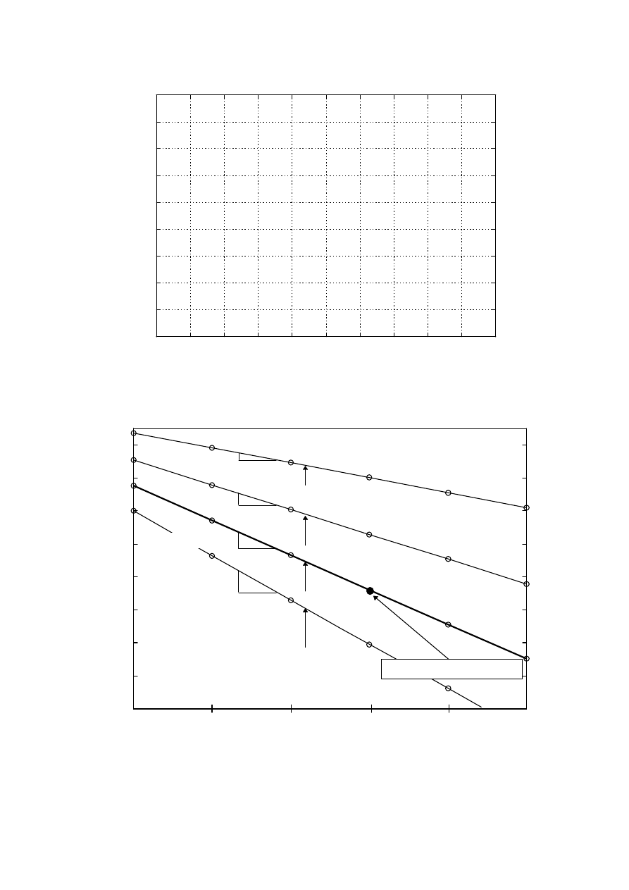
For each octave increase of the oversampling ratio, the modulator exhibits a 6n+3 dB decrease
in in-band noise power, where n is the number of filter notches [2]. The theoretical results of
inband noise levels for different number of loops and oversampling ratios are given in Figure 3.
International Workshop on ADC Modelling (IMEKO), May 7-9, 1996, Smolenice Castle, Slovak Republic
___________________________________________________________________________________________________
Page 3
0
0.05
0.1
0.15
0.2
0.25
0.3
0.35
0.4
0.45
0.5 F
s
-180
-160
-140
-120
-100
-80
-60
-40
-20
|H(
ν
)| [dB]
0
Frequency normalised to the sampling Frequency Fs
Figure 2: Magnitude response of a 3-loop BP SD modulator for a composite 20 tones,
half-scale input signal.
256
128
64
32
16
8
Oversampling ratio
-180
-160
-140
-120
-100
-80
-60
-40
-20.7dB/octave
Modulator chosen for study
-26.8dB/octave
-9dB/octave
-15dB/octave
4-loops
3-loops
2-loops
1-loop
Figure 3:
In-band noise power for 2
nd
-, 4
th
-, 6
th
- and 8
th
-order BP SD modulator for a
single tone input signal.
International Workshop on ADC Modelling (IMEKO), May 7-9, 1996, Smolenice Castle, Slovak Republic
___________________________________________________________________________________________________
Page 4
In order to achieve the required 20-bit resolution conversion for a 14kHz bandwidth and
minimise the computation burden, a 6
th
-order BP
Σ∆
modulator was chosen. To achieve this
while maintaining appropriate SNR of 124.3dB or more a sampling frequency of 3MHz was
chosen (R=64). Employing a half full-scale input signal, the theoretical modulator SNR was
found to be 124.8dB. The decimation filter had to be designed so that the noise aliased into the
signal band did not increase the noise level by more than 0.5dB, with up to 1.4kHz transition
band and less than 4.5
µ
dB passband ripples. The modulator exhibits a 75mdB roll-off itself for
the composite tone input and a linear approximation of the quantizer which can be
compensated after decimation at the signal Nyquist rate with an appropriate compensation
filter or by careful design of the modulator coefficients.
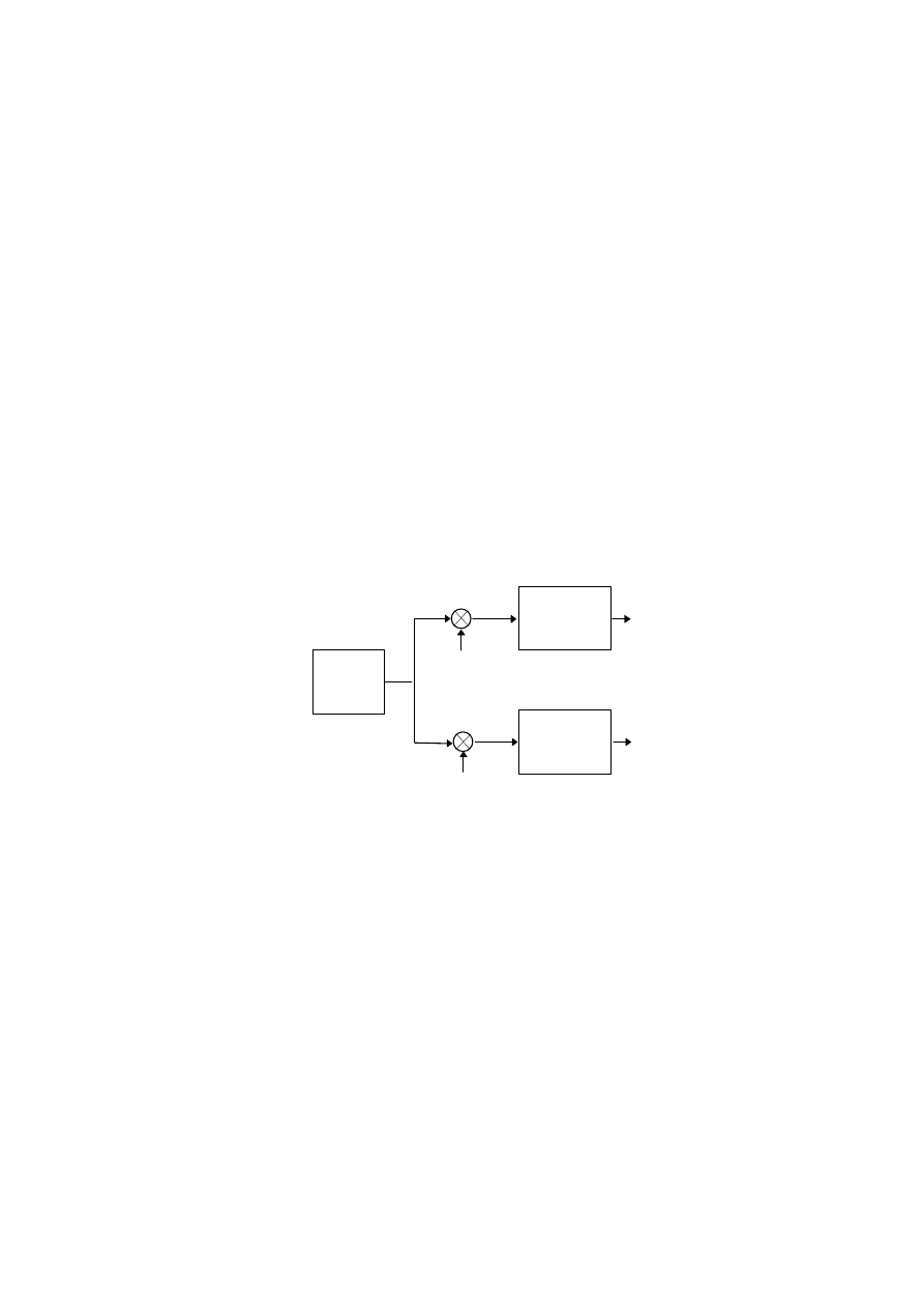
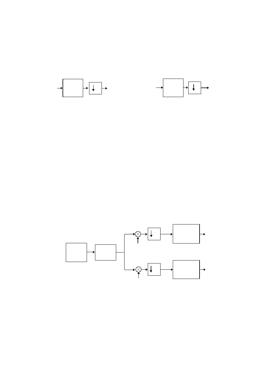
Bandpass Decimation
In bandpass
Σ∆
A/D converter the modulator is followed by a digital filter which converts
the high-speed bit-stream into a multi-bit output at the Nyquist rate. For bandpass modulation,
we need to perform narrow-band filtering on a high-speed bit-stream. We can modulate the
band of interest down to DC using e
-j2
π
fc
, where f
c
is the signal centre frequency, splitting the
modulator output into real and imaginary channels followed by a lowpass filter and sample rate
decreaser as in Figure 4 [1].
Polyphase
LPF
Decimator
Polyphase
LPF
Decimator
Bandpass
Σ∆
Modulator
-sin(
π
k/2) = 0, -1, 0, +1, 0, …
cos(
π
k/2) = +1, 0,- 1, 0, +1, …
Imaginary Channel
Real Channel
Figure 4
Modulator/decimator split into real and imaginary parts
For f
c
=0.25f
s
the sine and cosine sequences have very simple structure: each term is either 0
or ±1. Such multiplicands can be done by simple Boolean operations. Then the decimation can
be done with lowpass filters, identical for both real and imaginary channels, combined with the
sample rate decreaser. In our case a two-path polyphase structure is used to perform the
lowpass filtering [3]-[4].
All-Pass Two-Path Polyphase Approach
The basic recursive (IIR) N-D form second-order allpass filter A(z
-2
) (Figure 5a) in a
polyphase two-path configuration, with the appropriate delay in one of the branches, and their
purpose-designed coefficients result in very high-performance and easily implemented half-
band filters described by (5) and shown in Figure 5b, suitable for two-times decimation.
International Workshop on ADC Modelling (IMEKO), May 7-9, 1996, Smolenice Castle, Slovak Republic
___________________________________________________________________________________________________
Page 5
( )
( )
( )
(
)
( )
( )
H z
A z
z A z
A
z
z
A
z
i
j
j
i
=
+
=
+
−
−
−
−
−
−
∑
∑
1
2
1
2
1
2
1
2
2
1
2
1
2
2
,
,
(5)
A
1
(z
-2
)
A
2
(z
-2
)
z
-1
Σ
0 . 5
α
Σ
+
-
Σ
z
-1
z
-1
Figure 5
N-D form allpass filter (a), two-path half-band lowpass filter suitable for two-
times decimation (b).
In our design in order to achieve higher attenuation, we use two such filters in each
decimation stage. Higher even-order filters can be realised by cascading a number of allpass
filters. The chosen allpass filter structure performs filtering with minimum number of
calculations. It ensures that for input limited to unity, the relative peak gains at intermediate
points in the structure will not exceed 2. Design techniques for such filters employing parallel /
cascade combinations of elementary all-pass sections having one coefficient per second-order
stage, as the starting point for an eventual elliptic approximation, have been reported in depth
in [3]. The algorithm for generating allpass filter coefficients is fairly straightforward for
floating-point coefficients. However, for effective real-time physical realisations fixed-point
finite wordlength coefficients are required.
X(z)
A
1
(z
-1
)
A
2
(z
-1
)
Σ
0 . 2 5
Y(z)
A
1
(z
-1
)
A
2
(z
-1
)
Σ
Σ
A
1
(z
-1
)
A
2
(z
-1
)
f
s
Figure 6
Decimation by two using double polyphase lowpass filter
It should be noted that a sample-rate reduction inherent to the decimation process, takes
place at the end of each cascade block. The implication of this is that the computations are
performed at higher rates. Subsequently half of the computed samples are thrown away. Since
the transfer functions of allpass filters involve only polynomials in z
-
2
, the sample rate
reduction can be moved to the input of the cascade blocks. The unit delay in the lower branch
is effected by staggering the undersampling and feeding even samples into the top branch and
odd samples into a lower branch [4]. Figure 6 shows the double lowpass decimation filter with
its sample-rate reduction at the input. The double delayors within the allpass sections (as
International Workshop on ADC Modelling (IMEKO), May 7-9, 1996, Smolenice Castle, Slovak Republic
___________________________________________________________________________________________________
Page 6
shown in Figure 2) are replaced with unit delayers working at twice lower rate. This basic
decimation structure has been used in each stage of the overall decimator cascade.
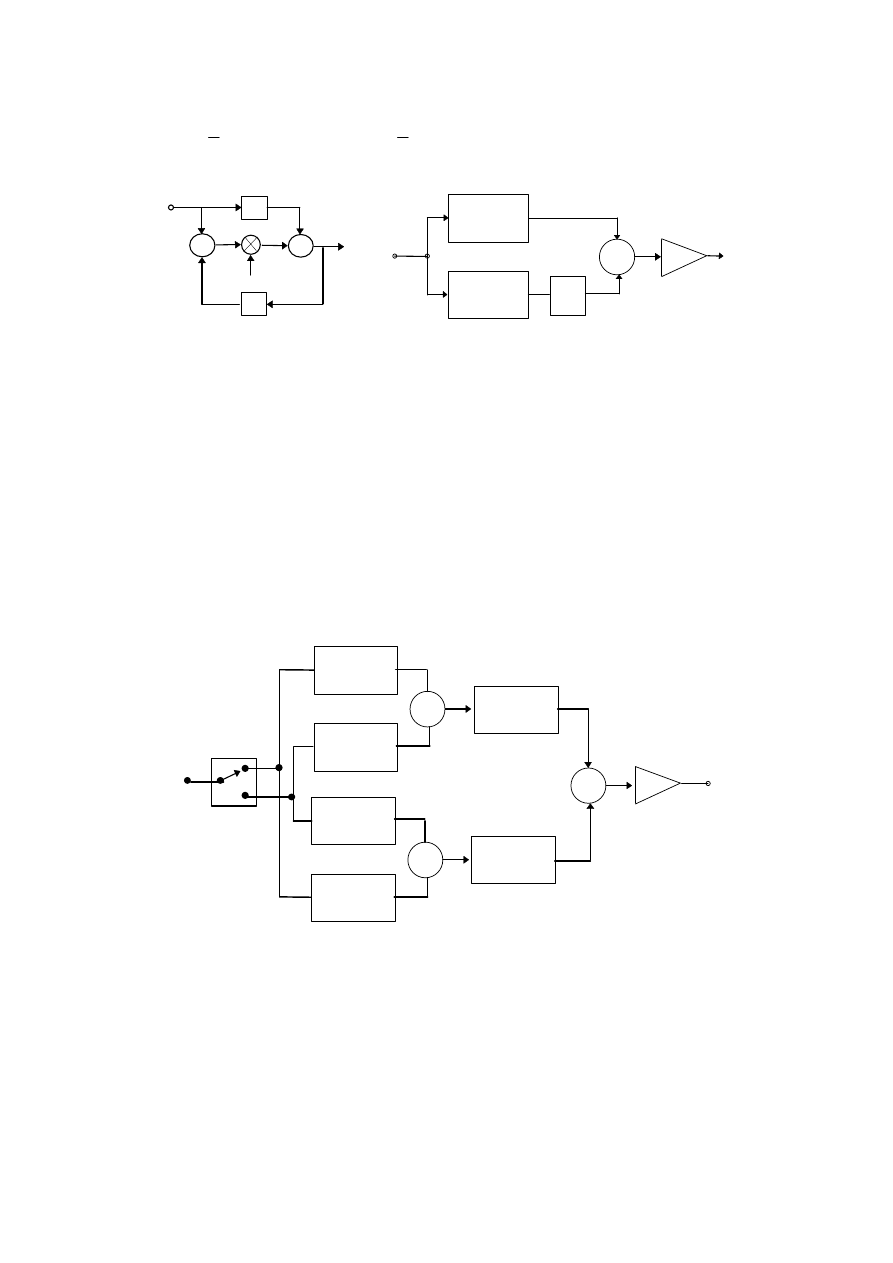
The Decimator Cascade Design
2
Stage 7
Double
Polyphase
LPF
Double
Polyphase
LPF
Stage 1
…
2
Figure 7
Cascaded decimator for single-sided AM signals
The overall decimation filter for single-sided AM signals in Figure 7 was constructed by
cascading the basic decimator blocks of Figure 6. Seven such stages were employed, providing
a lowpass sample-rate reduction of M=128. The decimation filter cascade, comprising double-
lowpass filter sections with two 4-bit wide (unsigned) coefficients (0.125, 0.5625) in stages
1 to 5, four 8-bit long (0.04296875, 0.17187500, 0.39453125, 0.74609375) in stage 6 and six
10-bit long (0.0810546875, 0.2763671875, 0.4990234375, 0.689453125, 0.833984375,
0.947265625) in stage 7. The filter coefficients were optimised by a specially developed "bit-
flipping algorithm" described later [5]. The out-of-band noise was attenuated 135.8dB in
stages 1 to 5, 146dB in stage 6 and 123.8 in stage 7. As a result the total quantization noise
aliased into the signal baseband was at a level of -133.8dB. The first five stages can be easily
implemented with hardwired shifts-adds as they require only 6 shift/add operations per stage.
Also, the first stage works with 1-bit data stream somewhat simplifying matters. In contrary, if
multiplications in stages 6 and 7 were performed through shifts-adds, they would require 51
operations for stage 6 and 96 for stage 7 employing 28-bit convergent-round arithmetic. There
calculations need to be performed by a specially designed arithmetic unit.
Last two
Stages of
Decimation
Last two
Stages of
Decimation
Double
Bandpass
Filter
-sin(
π
k/2) = 0, -1, 0, +1, 0, …
cos(
π
k/2) = +1, 0,- 1, 0, +1, …
Imaginary Channel
Real Channel
Bandpass
Σ∆
Modulator
32
32
Figure 8
Alternative structure comprising first stages of decimation into frequency
transformed bandpass filter working at the high rate.
The first five stages of decimation can be integrated together into a bandpass filter working
at the high rate and the sampling rate decreaser by 32 incorporated after the demodulator. This
idea is given in Figure 8. The prototype polyphase lowpass filter (0.13349539733,
0.57730761228) having attenuation of 65dB each and transition band of 0.265f
s
was converted
into the bandpass filter through the lowpass-to-bandpass frequency transformation [6]. The DC
feature of the lowpass filter was shifted to half-Nyquist and the edge of its passband, originally
International Workshop on ADC Modelling (IMEKO), May 7-9, 1996, Smolenice Castle, Slovak Republic
___________________________________________________________________________________________________
Page 7
at 0.122f
s
, was used to create the bandwidth of 0.0078125f
s
. The resulting 10
th
-order IIR
bandpass filter transfer function was a function of z
-2
and had even symmetric denominator and
odd symmetric numerator. This lead to simplifying computations to only four floating-point
multiplications for both bandpass filters, but their coefficients had to be at least 22 bits long to
achieve the correct magnitude response. The last two stages of decimation were exactly the
same as in the previous structure. The overall performance of both structures was exactly the
same.
The resulting decimation filter output quantization noise power is the sum of the noise
introduced by the modulator into the signal baseband and its part aliased during the
decimation. The total baseband magnitude response passband ripples of the decimation filter, is
the sum of all lowpass filter passband ripples of all the stages and the noise spectrum aliased
into the signal band. For the case of a multistage decimation filter decreasing the sampling rate
by two at each stage, both output quantization noise power and decimation filter passband
ripples can be calculated at the end of each stage using the term of an "overall lowpass
transfer function" [4] given by (6), where
ν =
f f
s
is the normalised frequency.
( )
H
H
R
OTF
i
i
i
R
ν
ν
=
−
=
∏
2
1
0
2
log
(6)
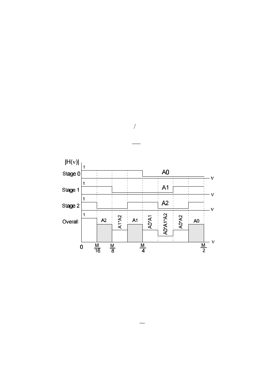
Figure 9
The three-stage decimator alias contributions
This idea is presented in Figure 9 for a three-stage decimation filter. For a small number of
decimation filter stages, the only significant noise aliasing into the baseband originates from the
modulator noise spectrum, at frequencies where only one low-pass filter has its stopband
replica. Then the noise power S
B
and the filter passband ripples PR at the end of the i
th
stage
can be computed using (7) and (8).
PR
Min
H
2
M
i
i
j
j 0
i
0 M2
log 2 M i
=
∈
−
+
=
∏
ϖ
,
ν
(7)
International Workshop on ADC Modelling (IMEKO), May 7-9, 1996, Smolenice Castle, Slovak Republic
___________________________________________________________________________________________________
Page 8
( )
( )
S
S
H
2
M
d
B
i
ee
i
j
j 0
i
0
M2
log 2M i
ν
ν
ν
ν
=
=
∏
∫
−
+
(8)
This enables us to design and optimise lowpass filters in each stage to its required
specification independently from its successive stages. If the performance of a given filter in the
cascade is better than required at the end of any one stage's optimisation, this fact is used to
advantage by relaxing the specification of the following stage, hence giving the possibility of
reduced implementation complexity.
It was important to find simple powers-of-two coefficients for use in the half-band
polyphase decimation filters. However, to find the relevant binary constrained coefficients
capable of satisfying the given decimator specification, a bit-flipping algorithm has been
developed [5]. It is seeded with the floating-point coefficients delivered from an elliptic
approximation [3]. A structured exhaustive search of the possible bit patterns yielding
improvement in the filter frequency response in question, starting from the most significant bit
of the fixed-point coefficient and working towards the least significant one, is at the heart of
this approach. The optimisation process starts with the first-stage filter in the decimator and
proceeds sequentially forward until the last stage is reached. If the attenuation achieved for the
required transition band for the given stage was better than it was assumed, this give rise to
relaxing the requirements for all the successive stages. The bit-flipping approach delivers more
efficient filters for a given wordlength in comparison to a truncated elliptic filter result [5].
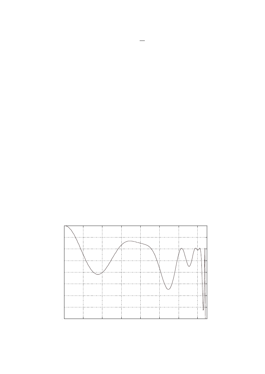
Decimation filter performance
The overall decimation filter performance is summarised in Figure 10 showing the overall
decimation filter passband ripples and Figure 11 giving the magnitude response at its output for
the 20-tone input through the modulator.
0
0.5
1
1.5
2
2.5
3
3.5 x 10
-3
F
s
-8
-7
-6
-5
-4
-3
-2
-1
0
|Η(ν)| [µ
dB]
Frequency normalised to the sampling frequency Fs
Figure 10 Overall decimation filter passband ripples

International Workshop on ADC Modelling (IMEKO), May 7-9, 1996, Smolenice Castle, Slovak Republic
___________________________________________________________________________________________________
Page 9
0
0.5
1
1.5
2
2.5
3
3.5 4x10
-3
F
s
-300
-250
-200
-150
-100
-50
|H(
ν
)| [dB]
0
Figure 11 Magnitude response of the decimator output for 20 tone input via the
modulator
The magnitude response of the bandpass filter (Figure 8) is given in Figure 12.
0
0.05
0.1
0.15
0.2
0.25
0.3
0.35
0.4
0.45
0.5 F
s
-350
-300
-250
-200
-150
-100
-50
|H(f)| [dB]
0
Figure 12 Magnitude response of bandpass filter output for 20-tones through the
modulator

International Workshop on ADC Modelling (IMEKO), May 7-9, 1996, Smolenice Castle, Slovak Republic
___________________________________________________________________________________________________
Page 10
As the bandpass filter was designed to be equivalent to the first five stages of the structure
in Figure 7, the overall noise and ripple performances of both structures are very close (not
distinguishable in Figure 10 and Figure 11). The obtained passband ripples were less than
±4
µ
dB with SNR=124.3dB, i.e. quantization noise level below 124dB (assuming half full-scale
input). For the structure from Figure 7 all calculations in first five stages can be done with
hardwired shift/add arithmetic units. The last decimation stages would require a specialised
type of processor similar to the one used in [4].
Conclusions
In this paper we have presented a sixth-order bandpass A/D converter potential of
conversion of bandpass (AM) signals centred at 455kHz with 14kHz bandwidth for up to 20-
bits of resolution. It employs bandpass
Σ∆
modulator sampled at 1.82MHz, transformed from
a lowpass prototype through z
z
→
-
2
transformation. This modulator coupled with a 7-stage
polyphase decimation filter delivered 124.3dB SNR with decimation filter passband ripples less
than 4
µ
dB. The use of polyphase structures in the decimation process allows minimisation of
the hardware complexity by using a small number of short-wordlength filter coefficients. The
simulation result indicates 124.3dB SNR with less than 4
µ
dB passband ripples for a half full-
scale composite input potential of up to 20-bit performance. The resultant converter directly
accomplishes demodulation of the narrow-band AM signals. The performance achieved by the
design and reported here are very difficult, if not impossible, to achieve by other means.
References
[1]
Schreier R. and W. M. Snelgrove, “Decimation for Bandpass Sigma-Delta Analogue-to-Digital
Conversion”, CH2868-8/90/0000-1801$1.00 © 1990 IEEE
[2]
Jantzi, S., R. Schreier and W. M. Snelgrove, “Bandpass Sigma-Delta Analog-to-Digital
Conversion”, IEEE Trans. On Circuits and Systems, vol. 38, no. 11, pp. 1406-1409, 1991
[3]
Valenzuela R. A. and A. G. Constantinides, "Digital Signal Processing Schemes for Efficient
Interpolation and Decimation", IEE Proceedings G, 1983, 130, (6), pp. 225-235
[4]
Kale, I, R. C. S. Morling, A. Krukowski and C.W. Tsang, "A high-fidelity decimator chip for
the measurement of sigma-delta modulator performance", IEEE Trans. on Inst. and
Measurement, vol. 44, no. 5, pp. 933-939, October 1995.
[5]
Krukowski, A., I. Kale, K. Hejn and R. C. S. Morling, "A Design technique for polyphase
decimators with binary constrained coefficients for high resolution A/D converters", IEEE Int.
Symposium on Circuits and Systems (ISCAS'94), Proc., Vol. 2, pp.533-536, 1994.
[6]
Constantinides A. G., "Spectral transformations for digital filters", IEE Proceedings, vol. 117,
no. 8, pp. 1585-1590, August 1970.
Wyszukiwarka
Podobne podstrony:
Principles of Sigma Delta Conversion for Analog to Digital Converters
Principles of Sigma Delta Conversion for Analog to Digital Converters
Principles of Sigma Delta Conversion for Analog to Digital Converters
On applications of Kalman filtering H Sorenson
61 881 892 Evaluation of PVD Coatings for Industrial Applications
94 1363 1372 On the Application of Hot Work Tool Steels for Mandrel Bars
Smarzewska, Sylwia; Ciesielski, Witold Application of a Graphene Oxide–Carbon Paste Electrode for t
Global Requirements for Medical Applications of Chitin and its Derivatives
Munster Application of an acoustic enhancement system for outdoor venues
Application of light emitting diodes for local lighting
Application of SPME for determination of organic vapours in
Application of binary immobilized Candida rugosa lipase for
Application of Data Mining based Malicious Code Detection Techniques for Detecting new Spyware
2 Application of Distributed Loads
2004 Code of Safe Practice for Solid Bulk?rgoesid 171
więcej podobnych podstron