1
Mikroskop elektronowy
[
edytuj
]
Z Wikipedii
Skocz do:
nawigacji
,
szukaj
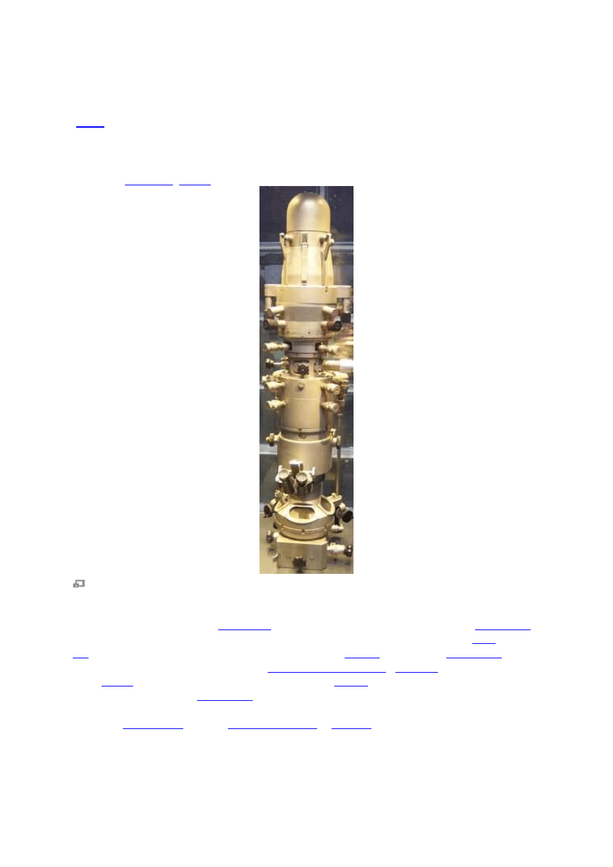
Elektronowy mikroskop transmisyjny
Mikroskop elektronowy —
mikroskop
wykorzystujący do obrazowania wiązkę
elektronów
,
który pozwala na dostrzeganie obiektów nawet milion razy cieńszych niż ludzki
włos
(0,1
nm
). Mikroskop elektronowy pozwala badać strukturę
materii
na poziomie
atomowym
.
Dzięki niemu możliwa jest obserwacja
organelli komórkowych
i
wirusów
. Próbka znajduje
się w
próżni
i najczęściej jest pokrywana warstewką
metalu
. Wiązka elektronów przemiata
badany obiekt i trafia do
detektorów
. Urządzenia elektroniczne odtwarzają na podstawie
zmierzonych sygnałów obraz badanej próbki. Pierwszy mikroskop elektronowy skonstruował
w 1931 r.
Ernst Ruska
razem z
Maksem Knollem
w
Berlinie
.
Spis treści

2
[
ukryj
]
•
1 Podstawy fizyczne
•
2 Typy mikroskopów elektronowych
o
2.1 Elektronowy mikroskop transmisyjny
o
2.2 Elektronowy mikroskop skaningowy
o
2.3 Mikroskop jonowy
•
3 Zastosowania
•
4 Zobacz też
Podstawy fizyczne
[
edytuj
]
Podstawowym parametrem mikroskopu jest
zdolność rozdzielcza
, która określa rozmiary
najmniejszych szczegółów jakie da się dostrzec w badanej próbce. Zdolność rozdzielczą
mikroskopu optycznego ogranicza
dyfrakcja
(
zjawisko fizyczne
zmiany kierunku
rozchodzenia się
fali
) promieni tworzących obraz. Im mniejsza jest długość fali, tym mniejszy
obiekt można obserwować. Granica rozdzielczości mikroskopu optycznego wynosi około 200
nm (z wyjątkiem
SNOM
).
W roku
1905
Albert Einstein
wyjaśnił zjawiska związane z
efektem fotoelektrycznym
,
proponując istnienie hipotetycznych cząstek światła nazwanych potem
fotonami
. Światło
ujawniło swoją
dwoistą naturę
. W pewnych sytuacja zachowuje się jak fala,w innych jak
strumień cząstek. W roku
1924
Louis de Broglie
zaproponował
hipotezę
, według której
cząstki elementarne miały podobną dwoistą naturę. Każda z nich jest zarówno cząstką jak i
falą, której długość zależy od
pędu
cząstki. Pęd fotonów jest niewielki i dlatego długość fali
świetlnej jest relatywnie duża w skali mikroświata. Nawet najlżejsze cząstki elementarne
mają pęd znacznie większy od fotonów. W ten sposób narodził się pomysł wykorzystania w
mikroskopii elektronów.
Pierwszy mikroskop elektronowy skonstruował w
1931
roku
Ernst Ruska
razem z
Maksem
Knollem
w
Berlinie
. Na Uniwersytecie w
Aberdeen
George Paget Thomson
przepuścił
wiązkę elektronów przez cienką folię metalową i zaobserwował obrazy dyfrakcyjne fal
materii. W Laboratoriach firmy Bell
Clinton Joseph Davisson
i
Lester Halbert Germer
prześwietli wiązką elektronów próbkę kryształu uzyskując obrazy dyfrakcyjne. W roku
1937
Thomson i Davisson wspólnie otrzymali za swoje prace
Nagrodę Nobla z fizyki
.
Typy mikroskopów elektronowych
[
edytuj
]
Ogólnie mikroskopy elektronowe można podzielić na zwykłe oraz skaningowe mikroskopy
elektronowe. W mikroskopach zwykłych jednocześnie analizowany jest duży obszar
powierzchni preparatu i tworzony jest jego obraz. W mikroskopach skaningowych w danym
momencie analizowany jest niewielki obszar, który jest traktowany jako punkt. Tworzenie
obrazu następuje poprzez zebranie informacji z kolejno analizowanych punktów.
Za pierwowzór i jednocześnie najprostszy mikroskop elektronowy uznawano (choć obecnie
rzadko jest wymieniany wśród mikroskopów elektronowych) jest
projektor elektronowy
zwany też mikroskopem polowym.
3
Elektronowy mikroskop transmisyjny
[
edytuj
]
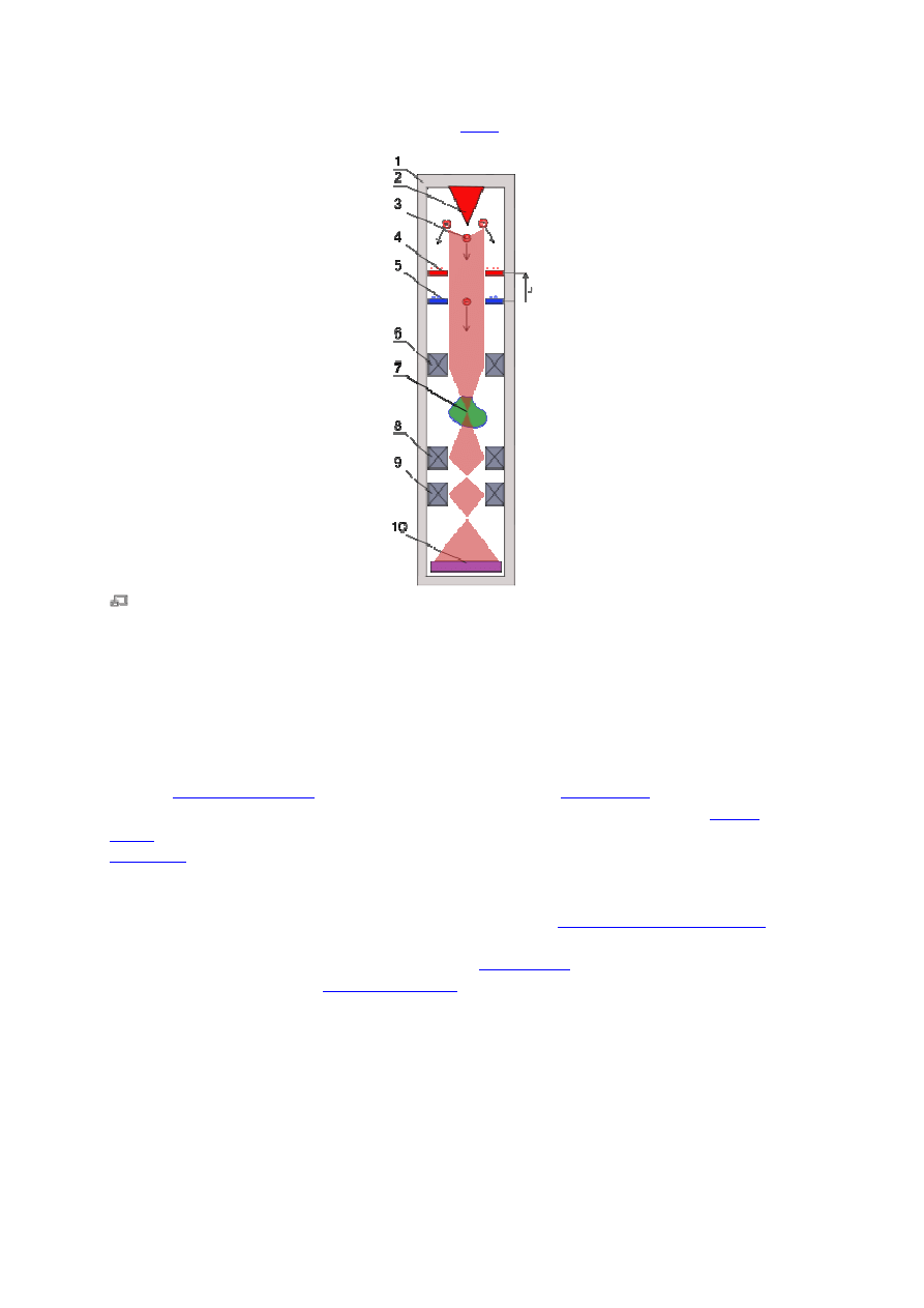
Uproszczony schemat mikroskopu elektronowego (mikroskop transmisyjnego)
Elektronowy mikroskop transmisyjny (en: Transmission Electron Microscope) - rejestrowane
są elektrony przechodzące przez próbkę. Próbka w takim mikroskopie musi być cienką płytką
o grubości mniejszej od 0,1 mikrometra. Przygotowanie takiej próbki jest trudne i znacznie
ogranicza zastosowania mikroskopu.
Najważniejszym elementem mikroskopu elektronowego jest kolumna mikroskopu (1), która
zawiera
działo elektronowe
(2) wytwarzające (np. w wyniku
termoemisji
) wiązkę
elektronów(3). Wstępnie uformowana wiązka elektronów w obszarze pomiędzy
katodą
(4) i
anodą
(5) zostaje rozpędzona uzyskując energię: E = eU, gdzie e jest ładunkiem elektronu, a U
napięciem
między katodą i anodą. Zwiększenie napięcia pozwala na zwiększenie pędu
elektronów, co zmniejsza długości fali. Przykładowo, gdy napięcie przyspieszające U=
300kV , wtedy długość fali elektronów λ = 0,00197 nm. Dla takiego napięcia prędkość
elektronów w kolumnie mikroskopu v =0,776c, gdzie c jest
prędkością światła w próżni
. Aby
elektrony mogły przebyć drogę od działa elektronowego do ekranu konieczne jest
utrzymywanie w kolumnie bardzo dobrej próżni.
Soczewkom
optycznym odpowiada
odpowiednio ukształtowane
pole magnetyczne
zmieniające bieg elektronów w cewkach
ogniskujących(6). Istotną zaletą soczewek magnetycznych jest możliwość płynnej zmiany ich
ogniskowych poprzez regulację natężenia prądu przypływającego przez soczewkę.
Gdy rozpędzona wiązka elektronów pada na preparat zachodzi szereg efektów, które są
wykorzystywane w różnych urządzeniach badawczych. W przypadku dostatecznie cienkich
preparatów część elektronów przechodzi przez preparat (7) i jest wykorzystywana w
transmisyjnych mikroskopach elektronowych. Elektrony mogą być odbite od preparatu lub
mogą wybijać z preparatu elektrony zwane wtórnymi. Te dwa rodzaje elektronów
wykorzystuje się w mikroskopach odbiciowych. Elektrony padające na preparat mogą

4
ponadto wzbudzać elektrony atomów badanej próbki, które następnie emitują rentgenowskie
promieniowanie charakterystyczne dla atomów próbki. Wiele mikroskopów elektronowych,
zarówno transmisyjnych jak i skaningowych, wyposażonych jest w spektrometr(y) EDS (en:
Energy Dispersive X-Ray Spectroscopy) i/lub WDS (en: Wavelength Dispersive X-Ray
Spectrometry), pozwalające na wykonanie analizy składu chemicznego próbki.
Wiązka elektronowa po przejściu przez preparat może być kształtowana podobnie jak
promienie świetlne, z wykorzystaniem układu
obiektyw
(8) -
okular
(9). W przypadku
elektronów zamiast szklanych elementów optycznych wykorzystywane są cewki zmieniające
bieg naładowanych cząstek. Mikroskop może pracować w trybie obrazu wówczas wiązka
tworzy obraz preparatu na detektorze (10). Mikroskop pracujący w trybie dyfrakcji może nie
mieć cewek obiektywu i okulary, obraz tworzą elektrony w wyniku zjawiska dyfrakcji na
strukturze próbki. W pierwszych konstrukcjach detektor był ekranem
elektronoluminescencyjny
(obecnie też stosowane), w obecnych konstrukcjach detektor w
postaci matrycy
CCD
, pobudzanej elektronami, umożliwia odczytanie obrazu jako sygnałów
elektrycznych, a odpowiednia aparatura pomiarowa pozwala na zapisywanie informacji i
tworzenie obrazu próbki.
Elektronowy mikroskop skaningowy
[
edytuj
]
SEM,
elektronowy mikroskop skaningowy
(en: Scanning Electron Microscope) -
rejestrowany jest potencjał lub prąd pomiędzy próbką a sondą skanującą - punkt po punkcie
dla całej próbki:
•
skaningowy mikroskop elektronowy emisyjny - rejestracja elektronów
przepływających pomiędzy sondą a próbką a emitowanych z sondy
•
skaningowy mikroskop polowy - emisja elektronów jest emisją polową, zachodzi w
wyniku silnego pola elektrycznego.
•
skaningowy mikroskop tunelowy
(
STM
, (en:Scanning Tunneling Microscope) - rodzaj
SPM
.
Mikroskop jonowy
[
edytuj
]
W celu zmniejszenia efektów falowych w miejsce elektronów używa się
jonów
.
Zastosowania
[
edytuj
]
Za pomocą mikroskopów elektronowych uzyskuje się niezwykle efektowne obrazy
praktycznie we wszystkich dziedzinach
nauki
. Ograniczeniem jest jednak konieczność
wykonywania pomiaru w próżni (problem w przypadku próbek biologicznych) oraz
przewodnictwo elektryczne próbki. W przypadku mikroskopii transmisyjnej wykonuje się
tzw. repliki: próbkę badaną napyla się (w tzw.
napylarce próżniowej
) cienką warstwą metalu
(najlepiej
złotem
) a następne usuwa oryginalną próbkę i wykonuje obraz repliki. W
przypadku mikroskopii skaningowej próbkę również napyla się
metalem
, ale nie trzeba
usuwać próbki właściwej. Zaletą tak uzyskanych zmodyfikowanych próbek jest ich trwałość i
możliwość powtarzania obrazowania, co nie zawsze możliwe jest w innych metodach
mikroskopowych.
5
Zobacz też
[
edytuj
]
•
działo elektronowe
•
mikroskop optyczny
•
SPM
(
mikroskop sił atomowych
i
skaningowy mikroskop tunelowy
)
•
Elektronowy mikroskop skaningowy
•
Mikroskop jonowy
Źródło: "
http://pl.wikipedia.org/wiki/Mikroskop_elektronowy
"
Kategoria
:
Mikroskopy
•
Tę stronę ostatnio zmodyfikowano 15:26, 26 kwi 2008.
•
Tekst udostępniany na licencji
GNU Free Documentation License
. (patrz:
Prawa
autorskie
)
Wikipedia® jest zarejestrowanym znakiem towarowym
Wikimedia Foundation
.
Możesz
przekazać dary pieniężne Fundacji Wikimedia
.
•
Zasady ochrony prywatności
•
O Wikipedii
•
Informacje prawne
Electron microscope
From Wikipedia, the free encyclopedia
•
Ten things you may not know about images on Wikipedia
•
Jump to:
navigation
,
search
This article needs additional
citations
for
verification
.
Please help
improve this article
by adding
reliable references
. Unsourced material may be
challenged
and removed. (November 2006)
An electron microscope is a type of
microscope
that uses
electrons
to illuminate a specimen
and create an enlarged image. Electron microscopes have much greater
resolving power
than
light microscopes
and can obtain much higher
magnifications
. Some electron microscopes can
magnify specimens up to 2 million times, while the best light microscopes are limited to
magnifications of 2000 times. Both electron and light microscopes have resolution limitations,
imposed by their wavelength. The greater resolution and magnification of the electron
microscope is due to the wavelength of an
electron
, its
de Broglie wavelength
, being much
smaller than that of a
light photon
,
electromagnetic radiation
.
6
The electron microscope uses
electrostatic
and
electromagnetic
lenses in forming the image
by controlling the electron beam to focus it at a specific plane relative to the specimen in a
manner similar to how a light microscope uses glass lenses to focus light on or through a
specimen to form an image.
Contents
[
hide
]
•
1 History
•
2 Electron microscope manufacturers
•
3 Types
o
3.1 Transmission Electron Microscope (TEM)
o
3.2 Scanning Electron Microscope (SEM)
o
3.3 Reflection Electron Microscope (REM)
o
3.4 Scanning Transmission Electron Microscope (STEM)
•
4 Sample Preparation
•
5 Disadvantages
•
6 Electron microscopy application areas
•
7 See also
•
8 References
•
9 External links
[
edit
] History
An image of an
ant
from a scanning electron microscope
The first electron microscope prototype was built in
1931
by the German engineers
Ernst
Ruska
and
Max Knoll
.
[1]
It was based on the ideas and discoveries of French physicist
Louis
de Broglie
[
citation needed
]
. Although it was primitive
[
citation needed
]
and not fit for practical use
[
citation
needed
]
, the instrument was still capable of magnifying objects by four hundred times.
Reinhold Rudenberg
, the research director of
Siemens
, had patented the electron microscope
in 1931, although Siemens was doing no research on electron microscopes at that time. In
1937 Siemens began funding Ruska and
Bodo von Borries
to develop an electron microscope.

7
Siemens also employed Ruska's brother
Helmut
to work on applications, particularly with
biological specimens.
[2][3]
In the same decade of 1930s
Manfred von Ardenne
pioneered the
scanning electron
microscope
and his universal electron microscope.
[4]
Siemens produced the first commercial TEM in 1939, but the first practical electron
microscope had been built at the
University of Toronto
in
1938
, by
Eli Franklin Burton
and
students Cecil Hall,
James Hillier
, and Albert Prebus.
[5]
Although modern electron microscopes can magnify objects up to two million times, they are
still based upon Ruska's
prototype
. The electron microscope is an integral part of many
laboratories. Researchers use it to examine biological materials (such as
microorganisms
and
cells
), a variety of large
molecules
, medical
biopsy
samples,
metals
and
crystalline
structures,
and the characteristics of various surfaces. The electron microscope is also used extensively
for inspection, quality assurance and failure analysis applications in industry, including, in
particular,
semiconductor device fabrication
.
[
edit
] Electron microscope manufacturers
Major manufacturers include:
•
Delong Group
•
FEI Company
– USA (merged with
Philips
Electron Optics)
•
FOCUS GmbH
– Germany
•
Hitachi
– Japan
•
Nion Company
- USA
•
JEOL Ltd.
– Japan (Japan Electro Optics Laboratory)
•
TESCAN
– EU
•
Carl Zeiss NTS GmbH
- Germany
[
edit
] Types
[
edit
] Transmission Electron Microscope (TEM)
Main article:
Transmission electron microscopy
The original form of electron microscopy,
Transmission electron microscopy
(TEM) involves
a high
voltage
electron beam emitted by a
cathode
, usually a tungsten filament and focused by
electrostatic and
electromagnetic
lenses. The electron beam that has been transmitted through
a specimen that is in part transparent to electrons carries information about the inner structure
of the specimen in the electron beam that reaches the imaging system of the microscope. The
spatial variation in this information (the "image") is then magnified by a series of
electromagnetic lenses until it is recorded by hitting a fluorescent screen, photographic plate,
or light sensitive sensor such as a CCD (
charge-coupled device
) camera. The image detected
by the CCD may be displayed in real time on a monitor or computer.
Resolution of the TEM is limited primarily by
spherical aberration
, but a new generation of
aberration correctors have been able to partially overcome spherical aberration to increase
resolution. Software correction of spherical aberration for the High Resolution TEM
HRTEM

8
has allowed the production of images with sufficient resolution to show carbon atoms in
diamond separated by only 0.89
ångström
(89
picometers
) and atoms in silicon at 0.78
ångström (78 picometers)
[6][7]
at magnifications of 50 million times.
[8]
The ability to determine
the positions of atoms within materials has made the HRTEM an important tool for nano-
technologies research and development.
[
edit
] Scanning Electron Microscope (SEM)
Main article:
Scanning Electron Microscope
Unlike the TEM, where electrons of the high voltage beam form the image of the specimen,
the
Scanning Electron Microscope
(SEM)
[9]
produces images by detecting low energy
secondary electrons which are emitted from the surface of the specimen due to excitation by
the primary electron beam. In the SEM, the electron beam is rastered across the sample, with
detectors building up an image by mapping the detected signals with beam position.
Generally, the TEM resolution is about an order of magnitude greater than the SEM
resolution, however, because the SEM image relies on surface processes rather than
transmission it is able to image bulk samples and has a much greater depth of view, and so
can produce images that are a good representation of the 3D structure of the sample.
[
edit
] Reflection Electron Microscope (REM)
In addition there is a Reflection Electron Microscope (REM). Like TEM, this technique
involves electron beams incident on a surface, but instead of using the transmission (TEM) or
secondary electrons (SEM), the reflected beam is detected. This technique is typically coupled
with
Reflection High Energy Electron Diffraction
and Reflection high-energy loss spectrum
(RHELS). Another variation is Spin-Polarized Low-Energy Electron Microscopy (SPLEEM),
which is used for looking at the microstructure of
magnetic domains
.
[10]
[
edit
] Scanning Transmission Electron Microscope (STEM)
Main article:
Scanning Transmission Electron Microscope
The STEM rasters a focused incident probe across a specimen that (as with the TEM) has
been thinned to facilitate detection of electrons scattered through the specimen. The high
resolution of the TEM is thus possible in STEM. The focusing action (and aberrations) occur
before the electrons hit the specimen in the STEM, but afterward in the TEM. The STEM's
use of SEM-like beam rastering simplifies
annular dark-field imaging
, and other analytical
techniques, but also means that image data is acquired in serial rather than in parallel fashion.
[
edit
] Sample Preparation
9
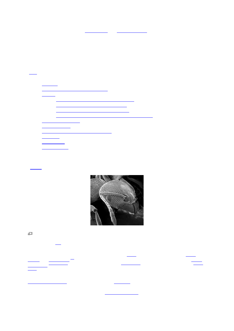
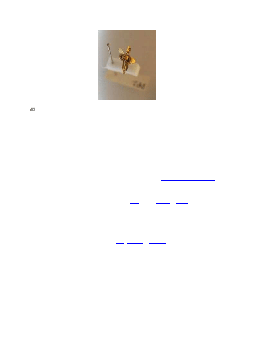
An insect coated in gold for viewing with a scanning electron microscope.
Materials to be viewed under an electron microscope may require processing to produce a
suitable sample. The technique required varies depending on the specimen and the analysis
required:
•
Fixation for biological specimens.
•
Cryofixation – freezing a specimen so rapidly, to
liquid nitrogen
or even
liquid helium
temperatures, that the water forms
vitreous (non-crystalline) ice
. This preserves the
specimen in a snapshot of its solution state. An entire field called
cryo-electron microscopy
has branched from this technique. With the development of
cryo-electron microscopy of
vitreous sections
(CEMOVIS), it is now possible to observe virtually any biological specimen
close to its native state.
•
Dehydration – replacing
water
with organic solvents such as
ethanol
or
acetone
.
•
Embedding – infiltration of the tissue with a
resin
such as
araldite
or
epoxy
for sectioning.
After this embedding process begins, the specimen must be polished to a mirror-like finish
using ultra-fine abrasives. The polishing process must be performed carefully to minimise
scratches and other polishing artefacts that impose on image quality.
•
Sectioning – produces thin slices of specimen, semitransparent to electrons. These can be cut
on an
ultramicrotome
with a
diamond
knife to produce very thin slices.
Glass knives
are also
used because they can be made in the lab and are much cheaper.
•
Staining – uses heavy metals such as
lead
,
uranium
or
tungsten
to scatter imaging electrons
and thus give contrast between different structures, since many (especially biological)
materials are nearly "transparent" to electrons (weak phase objects). In biology, specimens
are usually stained "en bloc" before embedding and also later stained directly after
sectioning by brief exposure to aqueous (or alcoholic) solutions of the heavy metal stains.
•
Freeze-fracture or freeze-etch – a preparation method particularly useful for examining lipid
membranes and their incorporated proteins in "face on" view. The fresh tissue or cell
suspension is frozen rapidly (cryofixed), then fractured by simply breaking or by using a
microtome while maintained at liquid nitrogen temperature. The cold fractured surface
(sometimes "etched" by increasing the temperature to about -100°C for several minutes to
let some ice sublime) is then shadowed with evaporated platinum or gold at an average
angle of 45° in a high vacuum evaporator. A second coat of carbon, evaporated
perpendicular to the average surface plane is often performed to improve stability of the
replica coating. The specimen is returned to room temperature and pressure, then the
extremely fragile "pre-shadowed" metal replica of the fracture surface is released from the
10
underlying biological material by careful chemical digestion with acids, hypochlorite solution
or SDS detergent. The still-floating replica is thoroughly washed from residual chemicals,
carefully fished up on EM grids, dried then viewed in the TEM.
•
Ion Beam Milling – thins samples until they are transparent to electrons by firing
ions
(typically
argon
) at the surface from an angle and sputtering material from the surface. A
subclass of this is
Focused ion beam
milling, where
gallium
ions are used to produce an
electron transparent membrane in a specific region of the sample, for example through a
device within a microprocessor. Ion beam milling may also be used for cross-section polishing
prior to SEM analysis of materials that are difficult to prepare using mechanical polishing.
•
Conductive Coating – An ultrathin coating of electrically-conducting material, deposited
either by high vacuum evaporation or by low vacuum sputter coating of the sample. This is
done to prevent the accumulation of static electric fields at the specimen due to the electron
irradiation required during imaging. Such coatings include gold, gold/palladium, platinum,
tungsten, graphite etc. and are especially important for the study of specimens with the
scanning electron microscope. Another reason for coating, even when there is more than
enough conductivity, is to improve contrast, a situation more common with the operation of
a FESEM (field emission SEM). When an osmium coater is used, a layer far thinner than
would be possible with any of the previously mentioned sputtered coatings is possible.
[3]
[
edit
] Disadvantages
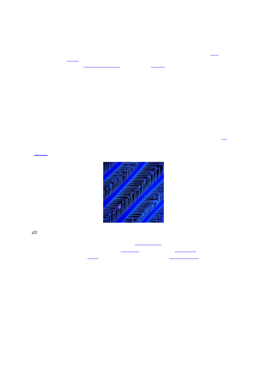
Pseudocolored SEM image of the feeding basket of
Antarctic krill
. Real electron microscope images
do not carry any color information, they are
greyscale
. The first degree
filter setae
carry in v-form
two rows of second degree
setae
, pointing towards the inside of the
feeding basket
. The purple ball
is one micrometer in diameter. To display the total area of this structure one would have to tile this
image 7500 times.
Electron microscopes are expensive to build and maintain. They are dynamic rather than static
in their operation: requiring extremely stable high-voltage supplies, extremely stable currents
to each electromagnetic coil/lens, continuously-pumped high- or ultra-high-vacuum systems,
and a cooling water supply circulation through the lenses and pumps. As they are very
sensitive to vibration and external magnetic fields, microscopes aimed at achieving high
resolutions must be housed in buildings (sometimes underground) with special services. Some
desktop low voltage electron microscopes have TEM capabilities at very low voltages (around
5 kV) without stringent voltage supply, lens coil current, cooling water or vibration isolation
requirements and as such are much less expensive to buy and far easier to install and

11
maintain, but do not have the same ultra-high (atomic scale) resolution capabilities as the
larger instruments.
The samples largely have to be viewed in
vacuum
, as the molecules that make up air would
scatter the electrons. One exception is the environmental scanning electron microscope, which
allows hydrated samples to be viewed in a low-pressure (up to 20
torr
), wet environment.
Scanning electron microscopes usually image conductive or semi-conductive materials best.
Non-conductive materials can be imaged by an environmental scanning electron microscope.
A common preparation technique is to coat the sample with a several-nanometer layer of
conductive material, such as
gold
, from a sputtering machine; however, this process has the
potential to disturb delicate samples.
The samples have to be prepared in many ways to give proper detail, which may result in
artifacts
from such treatment. This raises the problem of distinguishing artifacts from
material, particularly in
biological
samples. It is generally believed by scientists working in
the field that as results from various preparation techniques have been compared and that
there is no reason that they should all produce similar artifacts, it is reasonable to believe that
electron microscopy features correlate with living cells. In addition, higher-resolution work
has been directly compared to results from
X-ray crystallography
, providing independent
confirmation of the validity of this technique.
[
citation needed
]
Since the 1980s, analysis of unfixed,
vitrified specimens has also become increasingly used by scientists, further confirming the
validity of this technique.
[11]
,
[12]
,
[13]
[
edit
] Electron microscopy application areas
Semiconductor and
data storage
•
Circuit edit
•
3D metrology
•
Defect analysis
•
Failure analysis
Biology and life
sciences
•
Cryobiology
•
Protein localization
•
Electron
tomography
•
Cellular
tomography
•
Cryo-electron
microscopy
•
Toxicology
•
Biological
production
and
viral load
monitoring
Research
•
Materials qualification
•
Materials and sample
preparation
•
Nanoprototyping
•
Nanometrology
•
Device testing and
characterization
Industry
•
High-resolution imaging
•
2D & 3D micro-
characterization
•
Macro sample to
nanometer metrology
•
Particle detection and
characterization
•
Direct beam-writing
fabrication
•
Dynamic materials
experiments
•
Sample preparation

12
•
Particle analysis
•
Pharmaceutical QC
•
3D tissue imaging
•
Virology
•
Vitrification
•
Forensics
•
Mining
(
mineral liberation
analysis
)
•
Chemical
/
Petrochemical
[
edit
] See also
•
Category:Electron microscope images
•
Field emission microscope
•
Scanning tunneling microscope
[
edit
] References
1.
^
Ernst Ruska Nobel Prize autobiography
2.
^
Ernst Ruska (1986).
Ernst Ruska Autobiography
(English)
. Nobel Foundation. Retrieved on
2007
-
02-06
.
3.
^
DH Kruger, P Schneck and HR Gelderblom (13). "
Helmut Ruska and the visualisation of
viruses
" (in English). The Lancet 355 (9216): 1713-1717.
doi
:10.1016/S0140-6736(00)02250-
9
.
4.
^
M von Ardenne and D Beischer (1940). "Untersuchung von metalloxud-rauchen mit dem
universal-elektronenmikroskop" (in German). Zeitschrift Electrochemie 46: 270-277.
5.
^
MIT biography of Hillier
6.
^
OÅM: World-Record Resolution at 0.78 Å
, (May 18, 2001) Berkeley Lab Currents.
7.
^
P. D. Nellist, M. F. Chisholm, N. Dellby, O. L. Krivanek, M. F. Murfitt, Z. S. Szilagyi, A. R.
Lupini, A. Borisevich, W. H. Sides, Jr., S. J. Pennycook (17). "
Direct Sub-Angstrom Imaging of a
Crystal Lattice
" (in English). Science 305 (5691): 1741.
doi
:
10.1126/science.1100965
.
8.
^
The Scale of Things
, DOE Office of Basic Energy Sciences (BES).
9.
^
SCANNING ELECTRON MICROSCOPY 1928 - 1965
10.
^
[1]
11.
^
[ADRIAN, M., DUBOCHET, J., LEPAULT, J. AND MCDOWALL, A. W. (1984). Cryoelectron
microscopy of viruses Nature 308, 32-36.]
12.
^
[2]
13.
^
[S. Kasas, G. Dumas, G. Dietler, S. Catsicas, M. Adrian (2003) Vitrification of cryoelectron
microscopy specimens revealed by high-speed photographic imaging Journal of Microscopy
211 (1) , 48–53 doi:10.1046/j.1365-2818.2003.01193.x ]
[
edit
] External links
•
Environmental Scanning Electron Microscope (ESEM)
•
X-ray element analysis in electron microscope
– Information portal with X-ray microanalysis
and EDX contents
•
John H.L. Watson: Very early Electron Microscopy in the Department of Physics, the
University of Toronto – A personal recollection
•
Rubin Borasky Electron Microscopy Collection, 1930-1988
Archives Center, National Museum
of American History, Smithsonian Institution.
•
electron microscopy
Website of the ETH Zurich: Very good graphics and images, which
illustrate various procedures.

13
•
Albert Lleal microphotography. Scanning Electron Microphotography Coloured SEM
Retrieved from "
http://en.wikipedia.org/wiki/Electron_microscope
"
Categories
:
Microscopy
|
Scientific techniques
|
Nanotechnology
Hidden categories:
Articles needing additional references from November 2006
|
All articles with
unsourced statements
|
Articles with unsourced statements since March 2008
|
Articles with
unsourced statements since February 2008
•
This page was last modified on 15 May 2008, at 02:25.
•
All text is available under the terms of the
GNU Free Documentation License
. (See
Copyrights
for details.)
Wikipedia® is a registered trademark of the
Wikimedia Foundation, Inc
., a U.S. registered
501(c)(3)
tax-deductible
nonprofit
charity
.
•
Privacy policy
•
About Wikipedia
•
Disclaimers
Wyszukiwarka
Podobne podstrony:
Mikroskopia elektronowa id 3018 Nieznany
Mikroskopia elektronowa id 3018 Nieznany
Echo elektroniczne id 149974 Nieznany
elektro 3 id 157863 Nieznany
elektra 4 id 157704 Nieznany
5 Pole elektrostatyczne id 397 Nieznany
elektrae1 id 157847 Nieznany
FALE ELEKTROMAGNETYCZNE id 1677 Nieznany
elektro 2 id 157860 Nieznany
Budowa Lampy Elektronowej id 94 Nieznany (2)
Obrobka elektroerozyjna id 3280 Nieznany
ELEKTROSTATYKA 2 id 159079 Nieznany
elektra 8 id 157752 Nieznany
O PODPISIE ELEKTRONICZNYM id 32 Nieznany
elektroliza 3 id 158085 Nieznany
Obwody elektryczne id 329051 Nieznany
angielski dla elektrykow id 640 Nieznany
więcej podobnych podstron