
Procesor Z80
Dariusz Chaberski
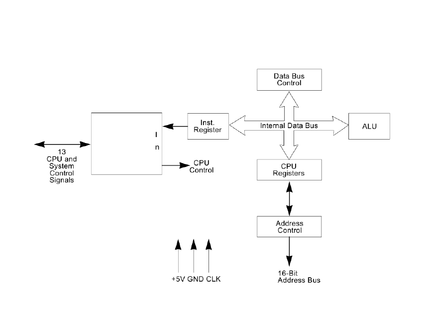
Z80 CPU Block Diagram
2
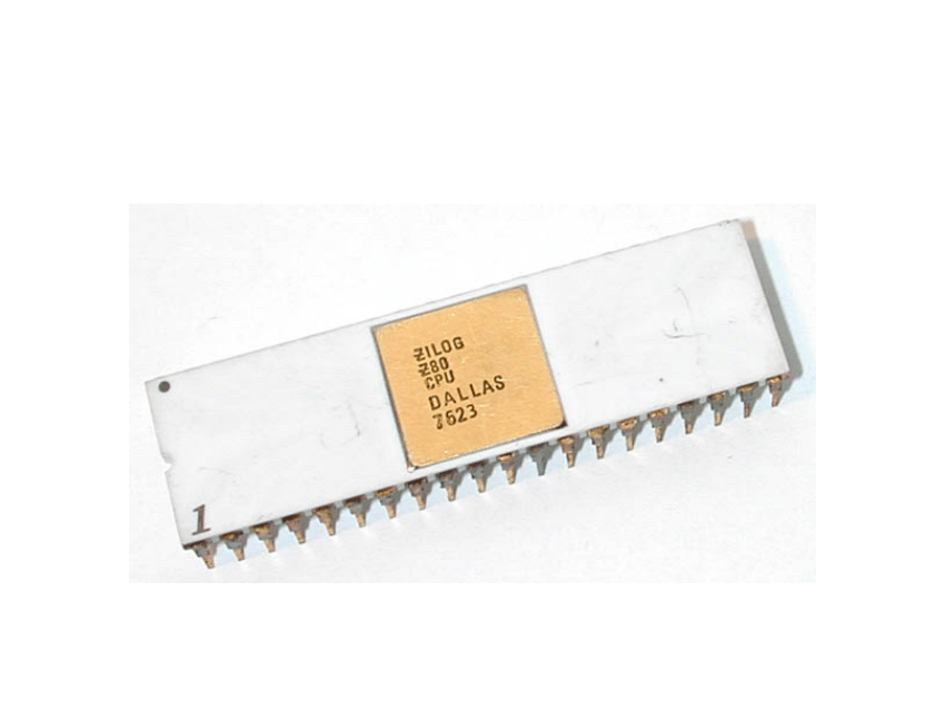
§ PDIP package
3
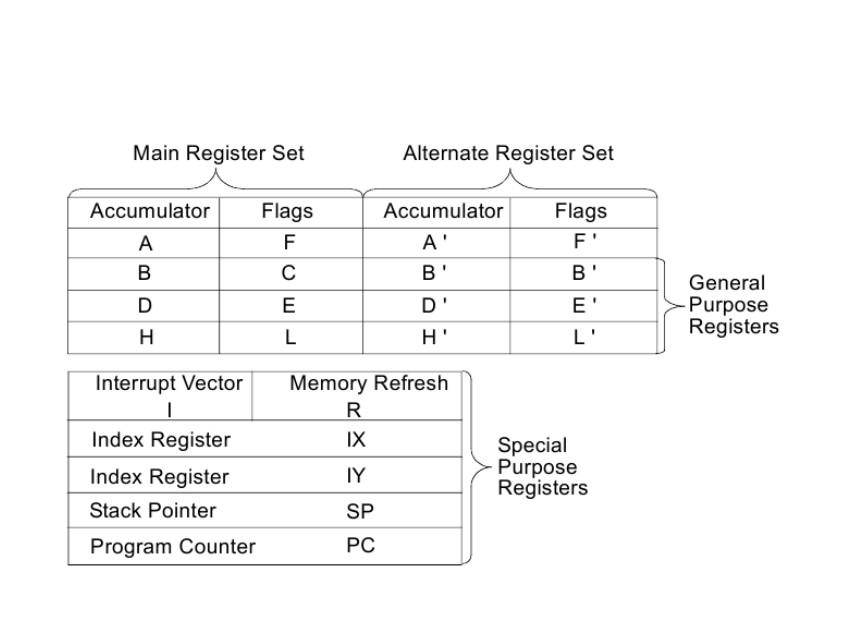
§ Z80 CPU Register Configuration
4
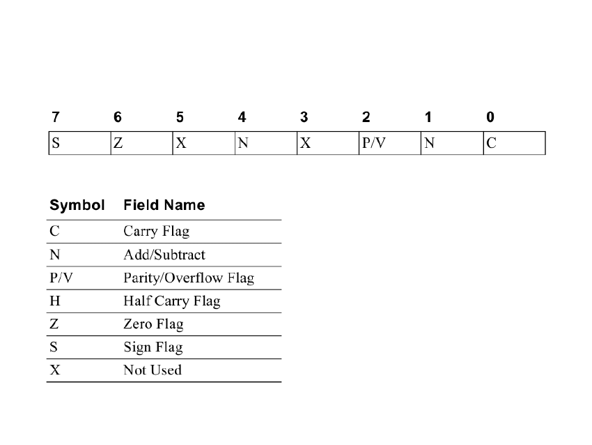
§ Z80 Status Indicator Flags
5
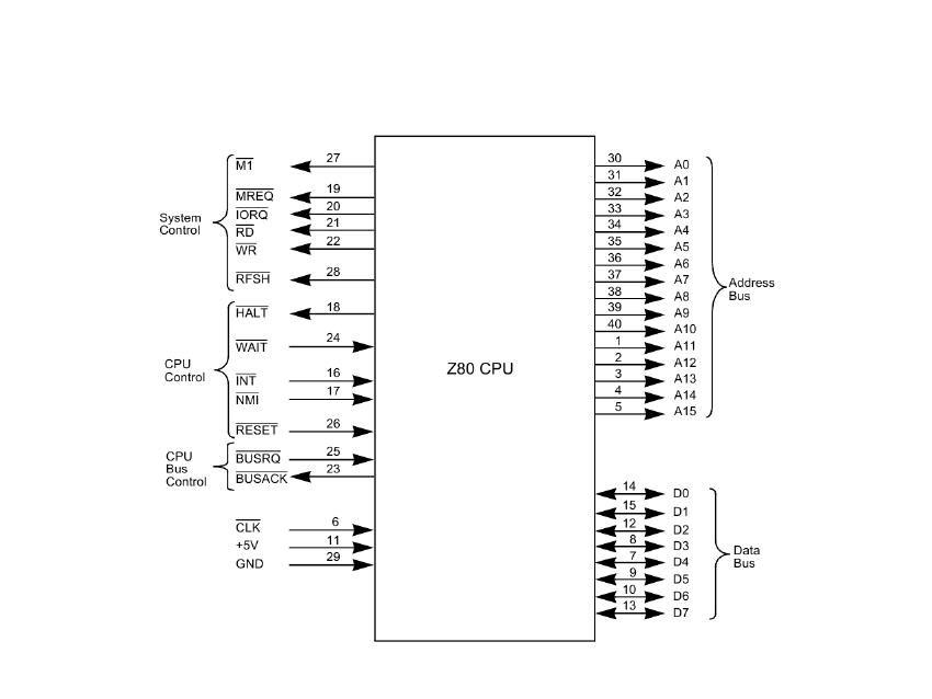
§ Z80 I/O Pin Configuration
6
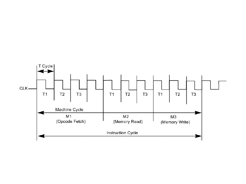
§ Basic CPU Timing Example
7
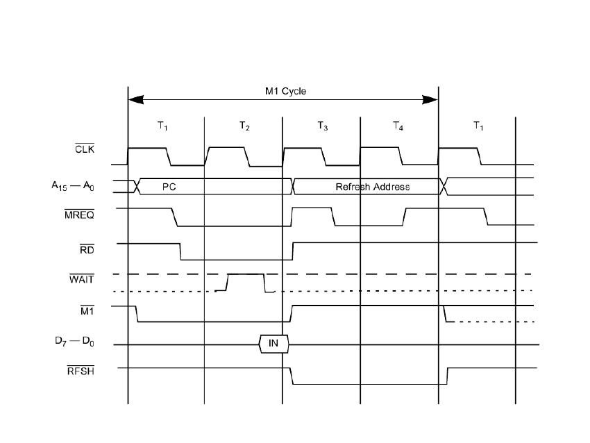
§ Instruction Op Code Fetch
8
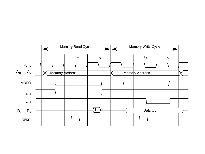
§ Memory Read or Write Cycle
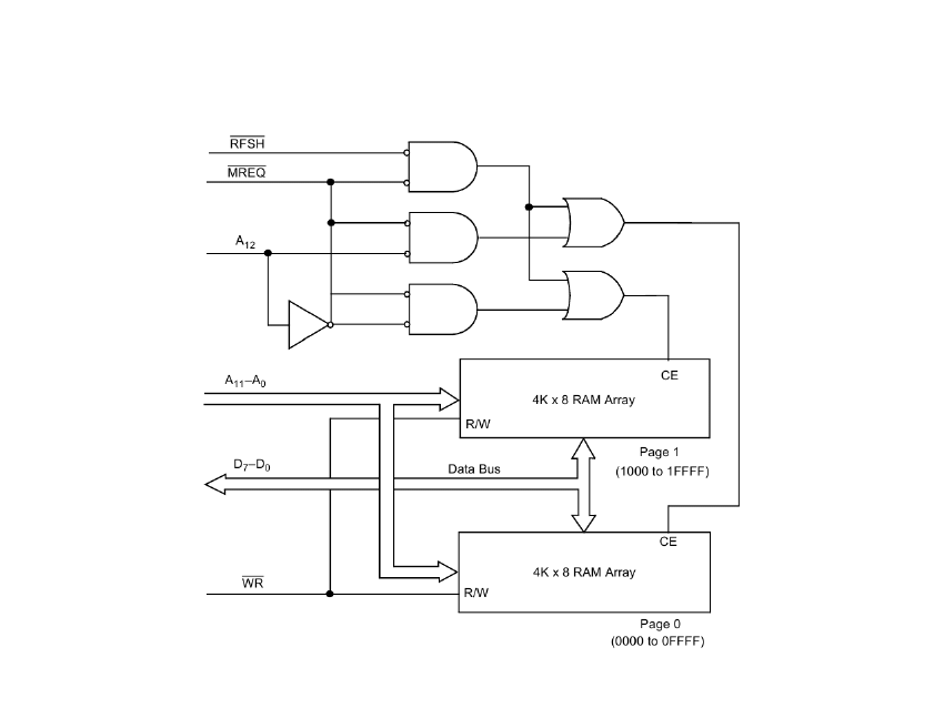
9
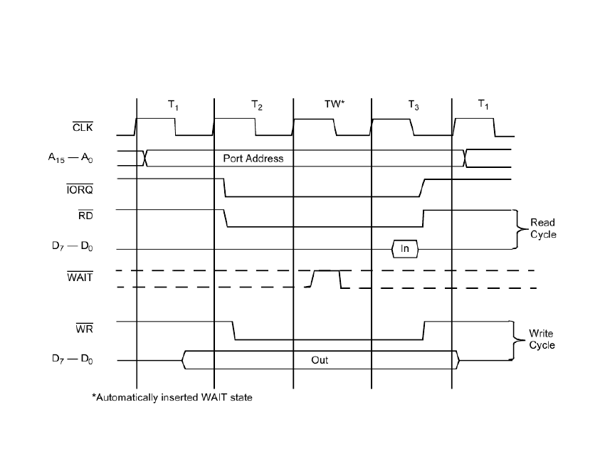
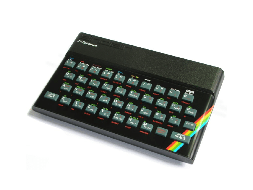
§ Input or Output Cycles
10
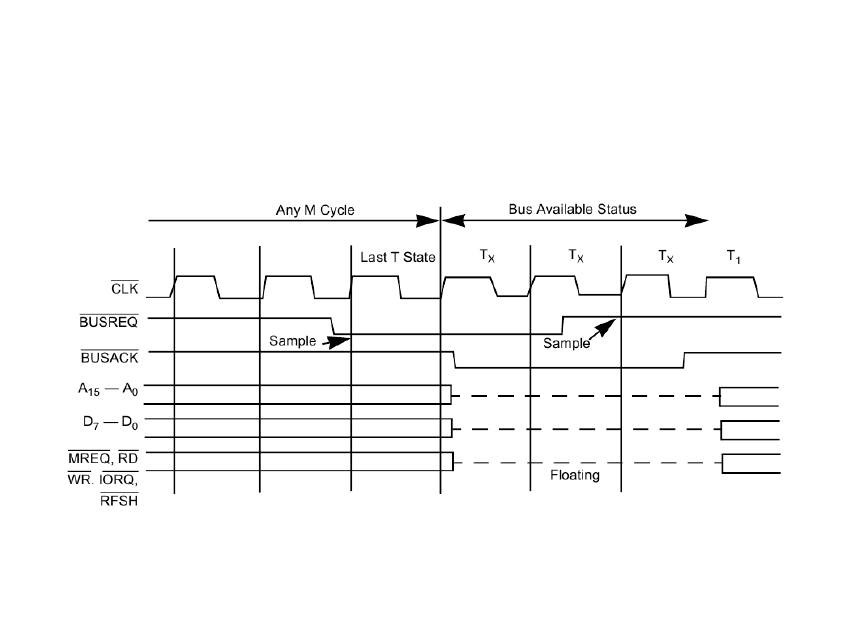
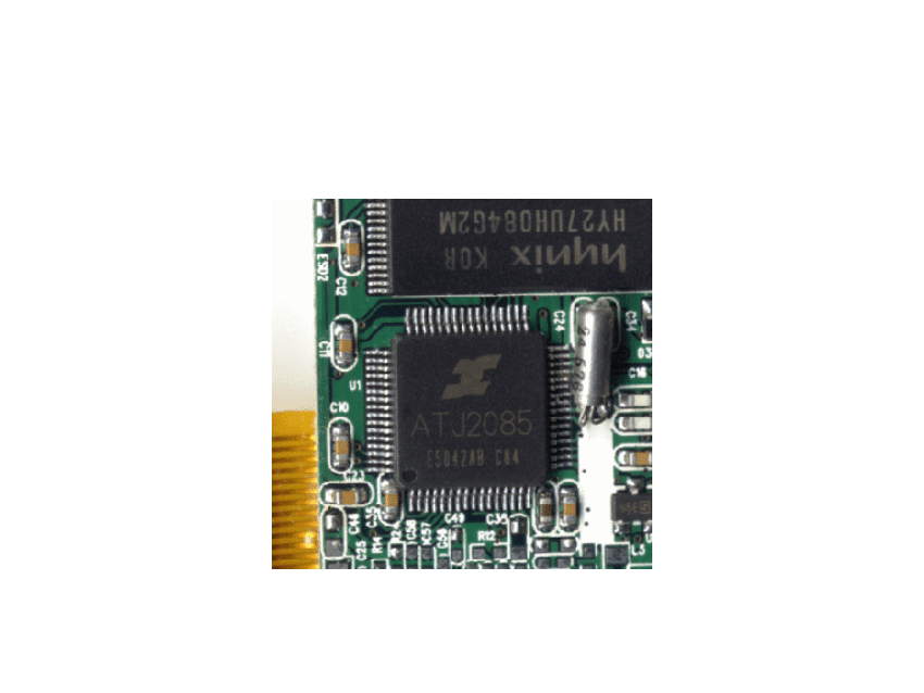
§ Bus Request/Acknowledge Cycle
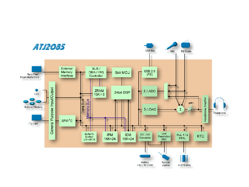
11
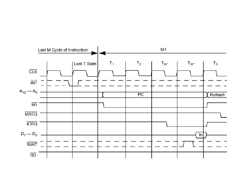
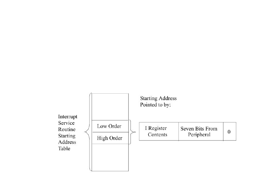
§ Interrupt Request/Acknowledge Cycle
12
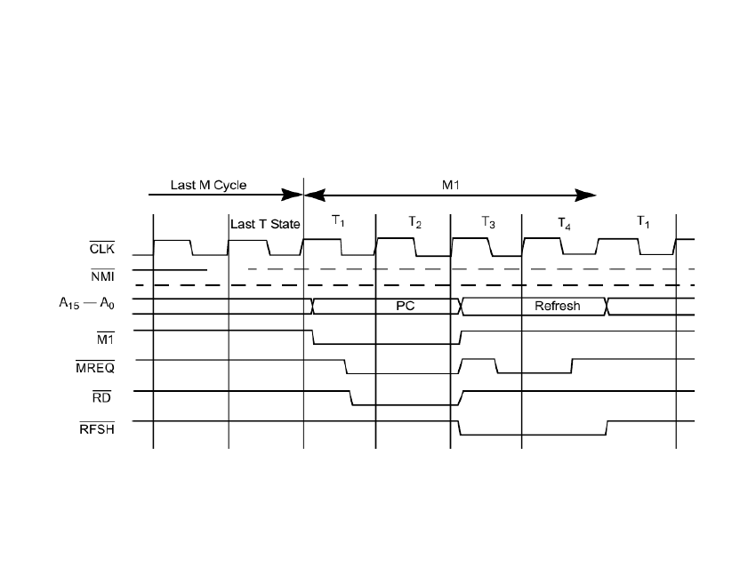
§ Non-Maskable Interrupt Request Operation
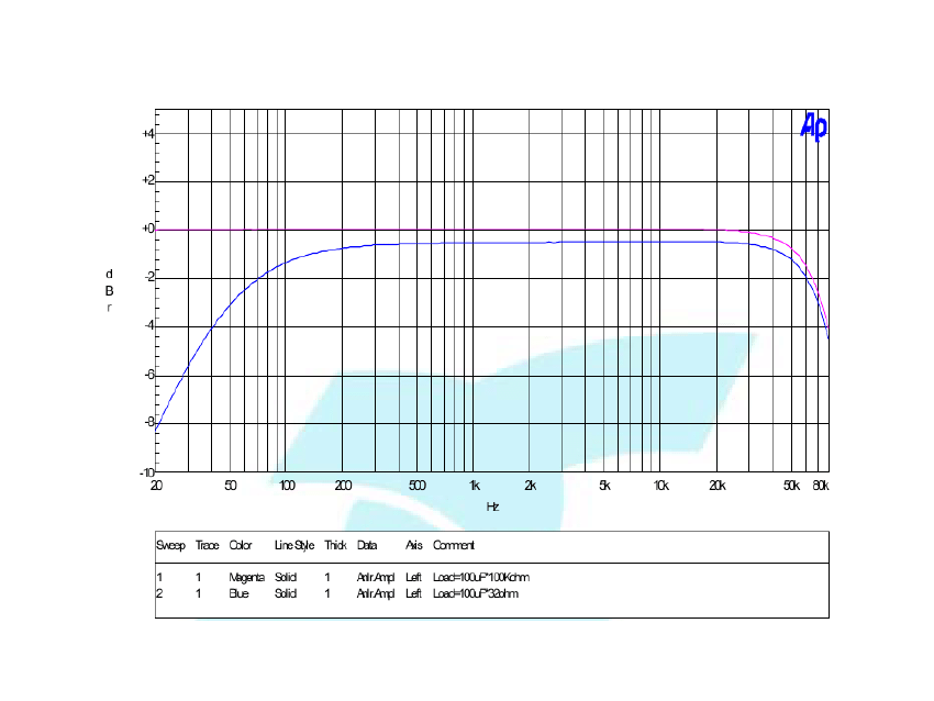
13
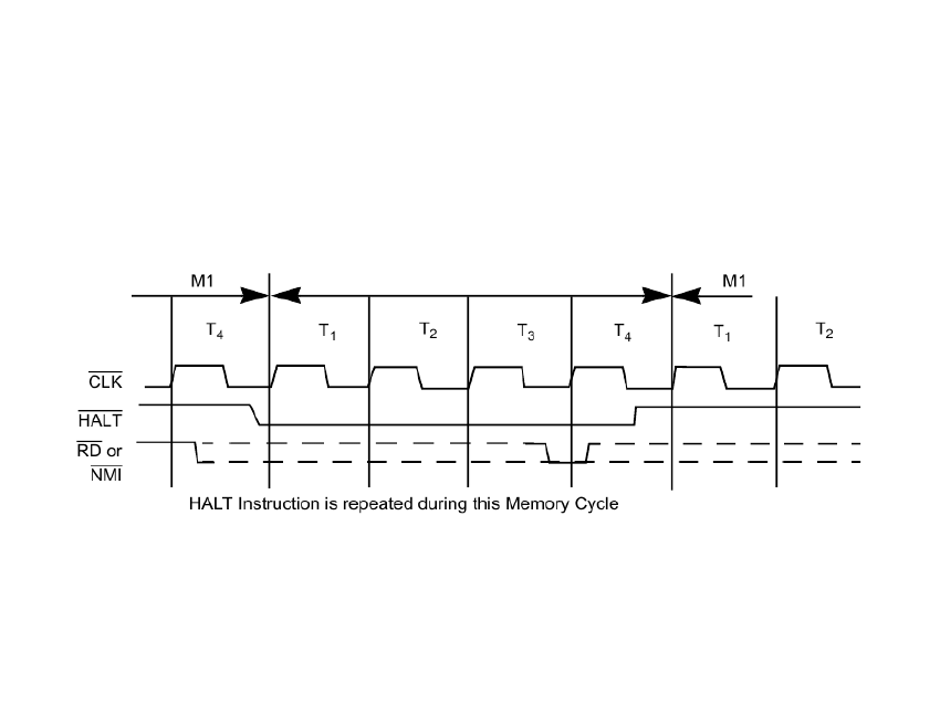
§ HALT Exit
14
§ Interrupts
+ Non-Maskable (restart to location 0066H)
+ Maskable
3 Mode 0 (8080 CPU Mode - 1-byte
RST p
instruction)
3 Mode 1 (restart to location 0038H)
3 Mode 2
15
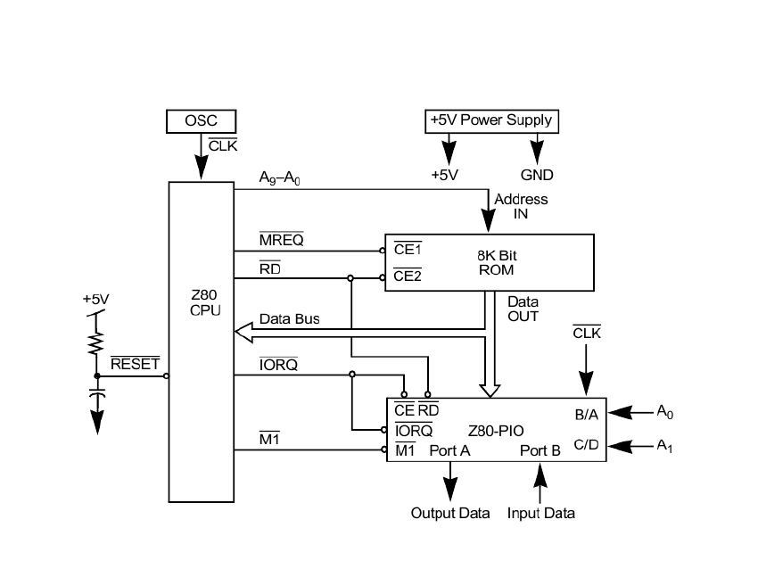
§ Minimum Z80 Computer System
16
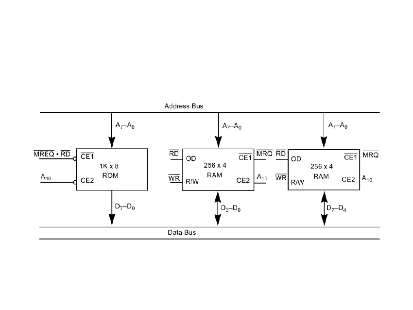
§ ROM and RAM Implementation
17
§ Interfacing Dynamic RAMs
18
§ ZX Spectrum
3.5 MHz, 48 kB, 256x192@4
19
20
ATJ2085
21
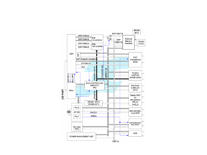
§ Functional Block Diagram
22
§ QFP package
23
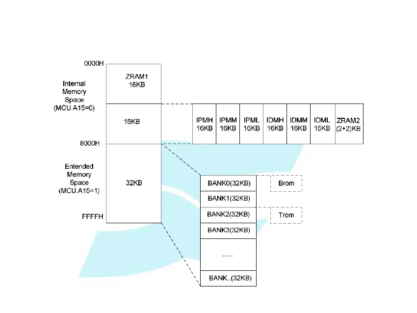
§ MCU 64 KB Memory Space
24
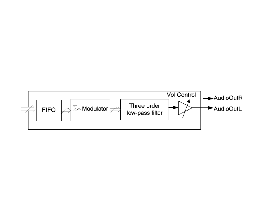
§ DAC
25
§ Frequency Response Diagram of Headphone Driver
26
Wyszukiwarka
Podobne podstrony:
Tryby przyjęcia przerwań przez procesor Z80
Konwersja szesnastkowo dziesietna za pomoca procesora Z80
Dzielenie liczb na procesorze Z80
stelmach od patrycji, 18 procesy demokratyzacyjne, 18
18 Prowadzenie procesów jednostkowych w technologii
18 Logistyka zaopatrzenia Analiza zapasów i procesów magazid 17872 ppt
18. post szczególne, Prawo karne procesowe
gleba procesy W 2011-10-18, gleboznawstwo, notatki
18 KOSZTY PROCESU I OPŁATY SĄDOWE
18 Maciejczak Dojrzalosc procesow
Ćwiczenie 18 & 19 Procesory Sygnalowe
18. Przebieg procesu umierania, MEDYCZNE, ANASTEZOLOGIA i PIEL ANSTZJOLOGICZNE
Notatka do slajdu 18 z prezentacji Proces badawczy
18. Zadania do procesu wychowania, Psychologia, Teoretyczne podstawy wychowania
Księga 1. Proces, ART 47(1) KPC, III CZP 85/07 - z dnia 18 października 2007 r
proces zarządzania zasobami ludzkimi (18 str)
więcej podobnych podstron