8281/8282
11/18/2002
Intended for analog and digital satellite receivers, the low noise block
converter regulator (LNBR) is a monolithic linear and switching voltage
regulator, specifically designed to provide the power and the interface
signals to the LNB downconverter via the coaxial cable.
If the device is in stand-by mode (EN terminal LOW), the regulator
output is disabled. This is to allow the antenna downconverters to be
supplied/controlled by other satellite receivers sharing the same coaxial
cable. In this mode the device will limit reverse current.
The A8281 is supplied in a 16-lead plastic SOIC with copper batwing
tab (suffix “LB”). The A8282 is supplied is a 24-lead plastic SOIC with
copper batwing tab (suffix “LB”). Operating temperature range is standard
classification (suffix "S").
The A8282 is available for improved power dissipation as well as
allowing direct replacement of Allegro’s first generation LNBR device, the
A8283SLB, with the exception of the bypass switch.
FEATURES
LNB selection and stand-by function
Built-in tone oscillator factory trimmed to 22 kHz facilitates DiSEqC™
encoding
Tracking switch-mode power converter for lowest dissipation
Externally adjustable short-circuit protection
LNB short-circuit protection and diagnostics
Auxiliary modulation input
Internal over temperature protection
Reverse current protection
Cable Length Compensation (A8282 only)
This device incorporates features that have patents pending.
Always order by complete part number:
Part Number
Package
A8282SLBTR
24 Lead SOIC Tape/Reel
A8282SLB
24 Lead SOIC
A8281SLB
16 Lead SOIC
ABSOLUTE MAXIMUM RATINGS
at TA = +25°C
Load Supply Voltage, VIN ...........................47 V
Output Current, I
OUT
............ Internally Limited*
Output Voltage, V
OUT
........................ -1V to 22 V
Switching Node, LX .......................................-1V
Logic Input ..................................... -0.3 V to 7 V
Package Power Dissipation (TA = +25°C), P
D
A8281SLB.......................... 56
°C/W**
A8282SLB.......................... 50
°C/W**
Operating Temperature Range,
T
A
................................ -20
°C to +85°C
Junction Temperature, T
J
......................... +150
°C
Storage Temperature Range,
T
S
............................... -55
°C to +150°C
* Output current rating may be limited by duty cycle,
ambient temperature, and heat sinking. Under any set of
conditions, do not exceed the specified current rating or a
junction temperature of 150
°C.
** Measured on a PCB with 2 oz copper with ground area
of 1 square inch.
LNB SUPPLY AND CONTROL
VOLTAGE REGULATOR
8281/8282
Diseq
Termination
Charge Pump
LX
Buck Converter
100uH
TSD
OverCurrent
LNB
VBULK
SENSE
VIN
-
+
135mV
-
+
-
+
900mV
Over-
Current
Output Voltage
Select
EXTM
TCAP
VSEL
1
Fault
GND
OLF
VPUMP
CPUM
P
PUM
P
X
352Khz
Divide
by 2
ENT
5V Regulator
Divide
by 16
EN
22 Khz Tone
Generation
+VIN
200 mohm
10nF
100nF
.1uF
.1uF
100uF
100uF
(8
2
8
2
o
n
ly
) VSEL
0
(8282 onl
y) LLC
(8282 Only)
VINT
.1uF
15
180uH
.22uF
4.7uF
Output Voltage Select Table – A8282SLB
VSEL0
VSEL1
LLC
VLNB
L
L
L
13
L
L
H
14
L
H
L
18
L
H
H
19
H
L
L
12
H
L
H
13
H
H
L
20
H
H
H
21
Output Voltage Select Table – A8281SLB
VSEL1
VLNB
L
13
H
18
8281/8282
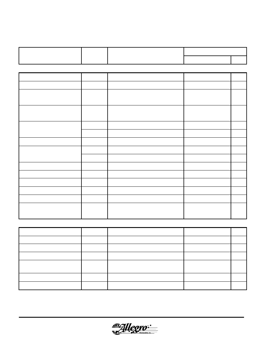
ELECTRICAL CHARACTERISTICS at T
J
= +125°C, C
LNB
= 100nF V
IN
=V
INMIN
to 47V (unless noted otherwise)
Limits
Characteristics
Symbol
Test Conditions
Min.
Typ.
Max.
Units
V
IN
Supply Voltage Range
V
INMAX
47
V
V
INMIN
4.5+Vo
Output Voltage
V
LNB
Relative to Voltage Select Table
I
LOAD
= 6mA to 750mA
-4.5
0
4.5
%
Output Voltage
V
LNB
ENT=H, I
LOAD
=12mA to 750mA
Average Voltage of LNB
-4.5
0
4.5
%
Vil
0.8
V
Logic Input Voltage
Vih
2.0
V
Logic Input Current
Iih
Vih=5 V
< 1.0
10
µA
Supply current
I
CC
EN = L
.25
1
mA
I
CCEN
EN = H, I
LOAD
= 0 mA
6
10
mA
Buck Switch On Resistance
R
DSBUCK
T
J
= 25
°
C, I
OUT
=750mA
.57
.67
Ω
T
J
=125
°
C, I
OUT
=750mA
.8
.94
Ω
Buck Switch Current Limit
I
BLIM
1
2.5
A
Switching frequency
fo
f
TONE
* 16
320
352
384
kHz
Linear regulator voltage drop
∆V
BUCK
V
SENSE
–Vo, ENT = L, I
LOAD
=750mA
700
900
1100
mV
Linear Regulator On Resistance
R
DSLNB
I
LOAD
= 750mA, VIN = 18V, T
J
= 25
°
C
Output Select = 18V
.375
Ω
Tone Characteristics
Tone Frequency
f
TONE
ENT=H
20
22
24
kHz
Tone Amplitude
A
TONE
ENT = H, I
LOAD
= 12mA to 750mA
0.4
.65
0.9
V
PP
Tone Duty Cycle
DC
TONE
I
LOAD
= 12mA to 750mA
40
60
%
Tone rise or fall time
tr, tf
ENT=H, I
LOAD
= 12mA to 750mA
5
10
15
µs
External Modulation Gain
g
EXTM
∆V
OUT
/∆V
EXTM
, f = 22 kHz square wave, I
LOAD
=
12mA to 750mA
4
5.0
6
V/V
EXTM Input Range
∆V
EXTM
Ac coupled
100
125
mVpp
External Modulation Impedance
Z
EXTM
f = 22kHz
4
10
k
Ω
NOTES: 1. Typical Data is for design information only.
2. Negative current is defined as coming out of (sourcing) the specified device pin.
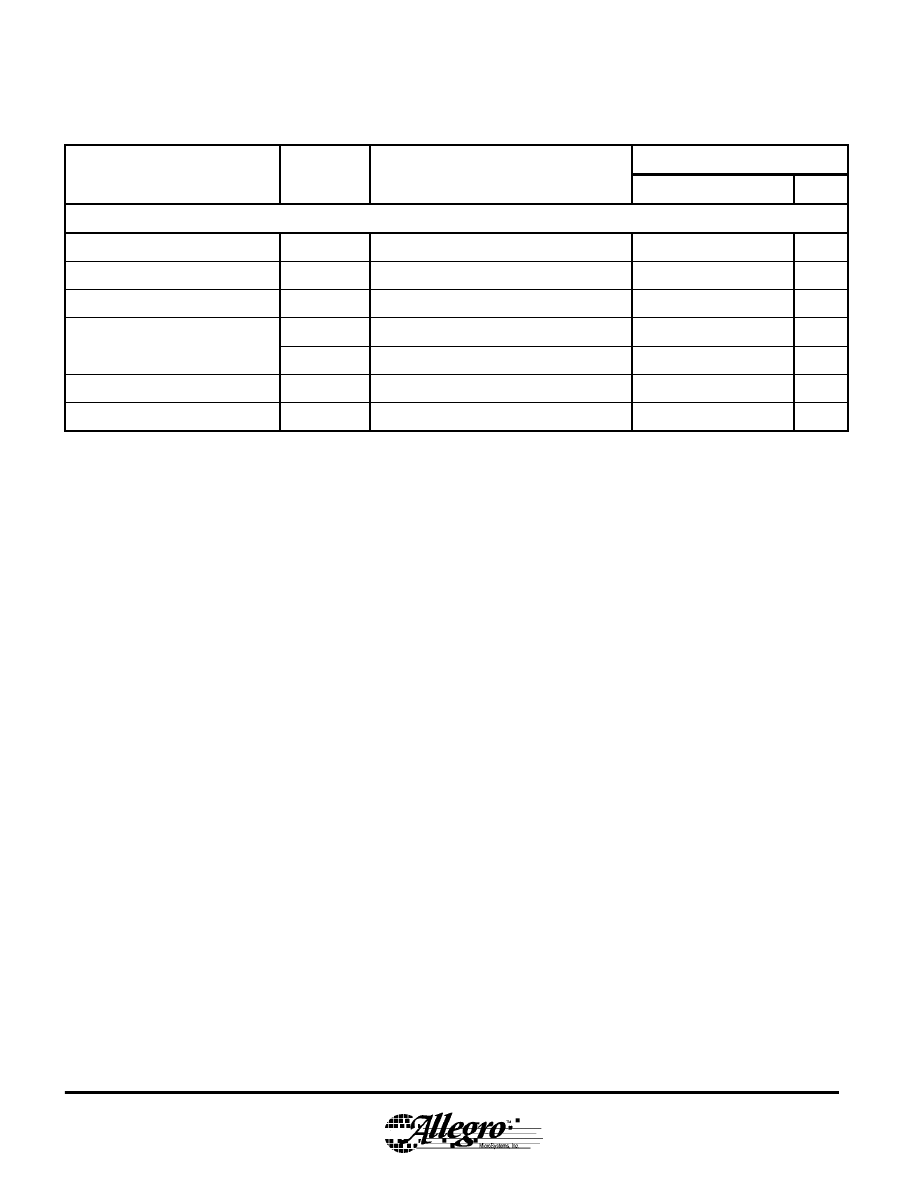
8281/8282
ELECTRICAL CHARACTERISTICS at T
J
= +125°C, C
LNB
= 100nF V
IN
=V
INMIN
to 47V (unless noted otherwise)
Limits
Characteristics
Symbol
Test Conditions
Min.
Typ.
Max.
Units
Protection Circuitry
Output Leakage Current
Ioz
Voh=5.5 V
< 1.0
10
µa
Overload flag terminal logic low
Vol
Iol=8 mA
0.28
.5
V
Output reverse current
I
OR
EN=L, V
LNB
= 22 V V
IN
=22 V or V
IN
floating
1.0
5
mA
Current Limiting Threshold
V
OMTH
115
135
155
mV
Thermal Shutdown Threshold
T
J
165
°C
Thermal Shutdown Hysteresis
∆T
J
20
°C
NOTES: 1. Typical Data is for design information only.
2. Negative current is defined as coming out of (sourcing) the specified device pin.

8281/8282
Functional Description
Buck Regulator.
A current-mode buck converter
provides the linear regulator a supply voltage that tracks the
requested LNB output voltage. The buck converter operates
at 16 times the internal tone frequency, nominally 352kHz.
The tracking regulator provides minimum power dissipation
across the range of output voltages by adjusting the SENSE
pin voltage 900 mV nominally above the LNB output
selected. The tracking Regulator also provides adequate
headroom for tone injection.
Linear Regulator.
The output linear regulator will sink
and source current. This allows tone modulation into a
capacitive load of 100nF for the output current range of
12mA to 750mA.
Slew Rate Control.
The programmed output voltage
rise and fall times can be set by an internal 25 k
Ω resistor
and an external capacitor located on the TCAP terminal. The
range of acceptable capacitor values is 4.7nF to 47nF. This
feature only affects the turn on and programmed voltage rise
and fall times. Modulation is unaffected by the choice of
TCAP. If LNB output voltage rise and fall time is not a
concern, the TCAP terminal should use a 100nF ceramic as
a default value to minimize output noise. If a small value
capacitor value is used, the rise time will be limited by the
time required to charge the VBULK capacitor.
Short Circuit Limit Regulator.
The LNB output is
current limited. The short-circuit protection threshold is set
by the value of an external resistor, R
SENSE
in conjunction
with an internal 135mV+/- 20mV reference voltage, V
OMTH
.
I
OM
= V
OMTH
/R
SENSE
The sense resistor should be chosen based on maximum DC
plus AC (tone), load current required, internal V
OMTH
tolerance, and sense resistor accuracy. For 750mA
applications, a precision 140mohm resistor is recommended.
For 500mA applications the resistor value can be raised to
200mohms.
In operation, the short-circuit protection produces current
limiting at the input due to the tracking converter. If the
output is shorted, the linear regulator will limit the output
current to I
OM
.
Fault Output.
Short-circuit or thermal shutdown will
cause the OLF terminal, an open-drain diagnostic output
flag, to go LOW.
Internal Tone Modulation.
The ENT (Tone Enable)
terminal activates the internal tone signal modulating the dc
output with a 650mV peak to peak, trapezoidal waveform.
The internal oscillator is factory trimmed to provide a tone
of 22 kHz +/- 2 kHz. No further adjustment is required.
Burst coding of the 22 kHz tone can be accomplished, due to
the fast response of the ENT input and rapid tone response.
This allows implementation of the DiSEqC™ protocols.
External Tone Modulation.
To improve design
flexibility and to allow implementation of proposed LNB
remote control standards, an analog modulation input
terminal is available (EXTM). An appropriate dc blocking
capacitor must be used to couple the modulating signal
source to the EXTM terminal. If external modulation is not
used, the EXTM terminal should be bypassed to ground via
a .1uF ceramic capacitor. The input amplitude should stay
within 100 to 125mVpp to guarantee the DiSEqC™
amplitude specification over the output current range.
8281/8282
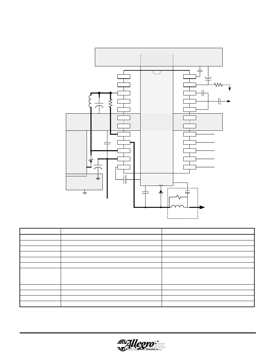
Typical Application Diagram
Optional
Diseq
Termination
C
LNB
15 Ohm
180uH
.22uF
EXTM
VINT
PUMPX
VPUMP
CPUMP
GND
GND
ENT
ENB
VSEL0
VSEL1
LLC
Rs
L1
C
BULK
C
IN
C
TCAP
+30V
D1
C
INT
C1
C2
C3
F-Connecter
Vin
D2
Control
Inputs
C
BYP
TCAP
R1
N/C
OLF
VBULK
N/C
N/C
GND
GND
SENSE
LNB
LX
VIN
TCAP
Description
Representative Component
C1-3, C
BYP,
C
LNB
.1uF/50V ceramic X7R/X5R
100uF Low ESR electrolytic 50V
Nichicon UHD1H101MPT
C
BULK
100uF Low ESR electrolytic/35V
Nichicon UHC1V101
C
INT
4.7uF/16V tantulum/electrolytic
D1
1.5A Schottky/40V or 50V
Sanken EK04
D2
1A Silicon Diode/25V
Sanken EU01
L1
100uH (750mA max Iload)
100uH (500mA max Iload)
TDK TSL1112-101K1R4
Falco D08018, Coilcraft DR0808,
TDK TSL0808-101KR80
L2
180uH (750mA Iload)
TDK TSL1112S-181K1R0-PF
RS
140-200mOhm sense resistor .25W
Meritek CR04R140F
C
TCAP
10nF ceramic X7R/X5R
R1
1M 5%

8281/8282
Component Selection.
Input Capacitor (C
IN
). An electrolytic should be located as
close to the device as possible. The input current is a square
wave with fast rise and fall times so the capacitor must be
able to handle the rms current without excessive temperature
rise. The value of the capacitor is not as important as the
ESR. The power dissipated in the input electrolytic is
Pd(C
IN
) = I
RMS
^2*ESR
The worse case Irms is with maximum I
LOAD
, minimum
VIN, and maximum V
OUT
(highest switch duty cycle).
Choose a capacitor with a ripple current rating greater than
I
LOAD
* 1.2*V
OUT(MAX)
/V
IN(MIN)
Buck Inductor (L1).
A 100uH power inductor is appropriate
for all operating conditions. The rated saturation current of
the inductor must be > 1.3A. The dc resistance should be
less than 350mohms, the smaller the better to maximize
efficiency.
Clamp Diode (D1). A schottky diode is required for the
switching node LX. The diode should be rated at 1.5 times
the maximum load current.
Output Capacitor (C
BULK
). A low ESR electrolytic is
recommended to minimize the Vpp ripple voltage. Less than
40mV Vpp is a reasonable goal.
Vpp =ESR*I
RIPPLE
I
RIPPLE
= (V
BULK
*(1-V
BULK
/V
IN
))/(L1*352khz)
Layout Notes.
1. Use a star ground approach. Connect the common
ground to the ground plane at the device ground pins.
The SOIC-24 has 2 pins on each side connected to the
package power ground tab. This allows the analog and
power ground to be kept separate on the PCB up to the
device.
2. Keep the sense resistor PCB trace as short and wide as
possible to lower trace resistance.
3. Connect the bypass capacitors as close to the device as
possible. The lower valued ceramic capacitors should be
closer to the device than electrolytics.
4. If using an unshielded power inductor for the buck
switch, place as far away from the device as possible.
The resulting EMI can result in additional noise on the
LNB output.
5. Place the TCAP capacitor as close to the device as
possible.
6. A two-sided board with ground planes on both sides of
the PCB will help optimize the power dissipation.
Typically several copper Vias under the device are used
to connect the ground planes and enhance thermal
performance.
Noise Immunity.
LNB systems can have a 50mV peak
specification for noise on the coaxial cable. This is easily
achievable with the A8282 with proper layout and following
a few guidelines.
1. Use a low ESR capacitor for VBULK, 400mohm
maximum is recommended.
2. The LNB output is sensitive to the TCAP reference pin.
Keep the PCB traces short and location of the bypass
capacitor close to the device. This pin is a high
impedance node and noise can be induced from the
proximity to an unshielded inductor. If the inductor can
not be placed far enough away to avoid this noise pickup,
it is important to ensure that the induced voltage is out of
phase with the switching node LX. Rotating the inductor
can change the phase of the induced voltage.
3. Be sure to place a 1uF to 10uF capacitor on internal
reference VINT.
4. Bypass the EXTM pin with a .1uF ceramic to GND.
5. Increasing output capacitance will attenuate noise,
however this must be traded off with the requirement for
low cable capacitance for 22khz-tone transmission.

8281/8282
Power Dissipation.
The power dissipated and
operating junction temperature of the 8281 and 8282 can be
estimated to ensure the device operates within desired
thermal budget.
The total chip power is contributed by three components.
Pd_bias = V
IN
* (I
CCEN
- 4mA)
Pd_buck = I
LOAD
^2 * R
DSBUCK
* V
BULK
/V
IN
Pd_lin = ∆V
BUCK
* I
LOAD
P
TOT
= Pd_bias + Pd_buck + Pd_lin
Where V
BULK
= ∆V
BUCK
+ I
LOAD
* R
SENSE
+ V
LNB
I
CCEN
, ∆V
BUCK
, and R
DSBUCK
can be taken from the
specification table. R
DSBUCK
is a function of
junction termperature. The R
DSON
will rise
approximately 2.7mohm/°C.
The junction temperature can be estimated by:
T
J
= P
TOT
*
R
ØJA
+
T
A
OR
T
J
= P
TOT
*
R
ØJT
+
T
TAB
Where R
ØJT
= 5.6°C /W
T
A
= Ambient Temperature °C
R
ØJA
= 50°C /W for A8282SLB
56°C /W for A8281SLB
R
ØJA
numbers for a typical two sided, 2 oz. copper, PC
board layout with copper ground plane of 1 square inch.
Additional copper ground plane area, multi- level boards, etc
can reduce the effective R
ØJA
.
DiSEqC
TM
.
The 22khz tone is specified to be compatible
to coaxial cable bus standards available from
www.eutelsat.com
. The A8282 LNB output will be able to
drive the DiSEqC termination network. This terminator
typically consists of a 180uH inductor, used to pass the dc
current with minimal loss, and a 15 ohm parallel resistor to
provide the recommended source impedance at 22khz.
Unidirectional communication systems such as DiSEqC 1.0
do not need this termination and the LNB output can be
directly connected to the coaxial cable.
13V to 18V Transition. The LNB output can be rapidly
switched between a high and low setting as a method of
receiver to LNB communication. The TCAP capacitor will
control the slew rate based on the RC charging.
t
RISE/FALL
= 25K*C
TCAP
*ln(V1/V2)
Small values of TCAP are used when the transition time is
desired to be less than a millisecond. In this case, the
minimum rise time is limited by the charge time of the
switching regulators output capacitor. This is dependent on
the LNB load current, peak current limit in the buck switch,
and the output amplitude change.
t
RISE
= C_bulk * (v2-v1)/(I_ave)
Where I_ave is the average current available to charge the
output capacitor and can be estimated by:
I_ave = 1.4A - I_load
Note that this is only a limitation due to the ability to charge
the output capacitor on a low to high change of the LNB
voltage. For high to low transitions, the output voltage will
be slew limited by TCAP.
The minimum value for TCAP should be 4.7nF.
8281/8282
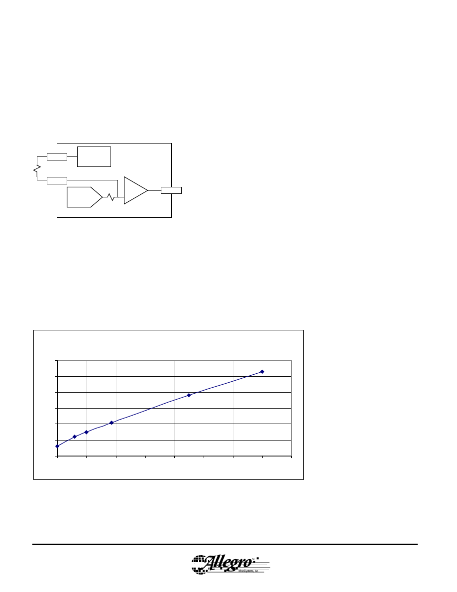
Output Voltage Adjust. It is possible to fine tune the LNB
output voltage to comply with the DirectTV specification by
connecting a 1M resistor from pin VINT to TCAP.
The LNB is output gained up by 6 from the TCAP voltage
as shown. The 1M resistor pulls the LNB voltage up 440mV
from the 13V nominal setting of the voltage select DAC by
sourcing approximately 2.76µA into the TCAP node.
TCAP
LNB
LNB Voltage
Select
VINT
25K
1M
Internal 5V
Reference
+
X 6
_
Capacitive Loading.
The linear regulator sink current
is limited which can cause overshoot of the 22Khz tone.
This effect only appears with low levels of output current
combined with high values of output capacitance. This
relationship is chart below. Points above the line will not
have excessive overshoot.
IOUT(ma) vs Cload (uf)
0.1
0.22
0.3
0.47
1
1.5
0
20
40
60
80
100
120
0.1
0.3
0.5
0.7
0.9
1.1
1.3
1.5
1.7
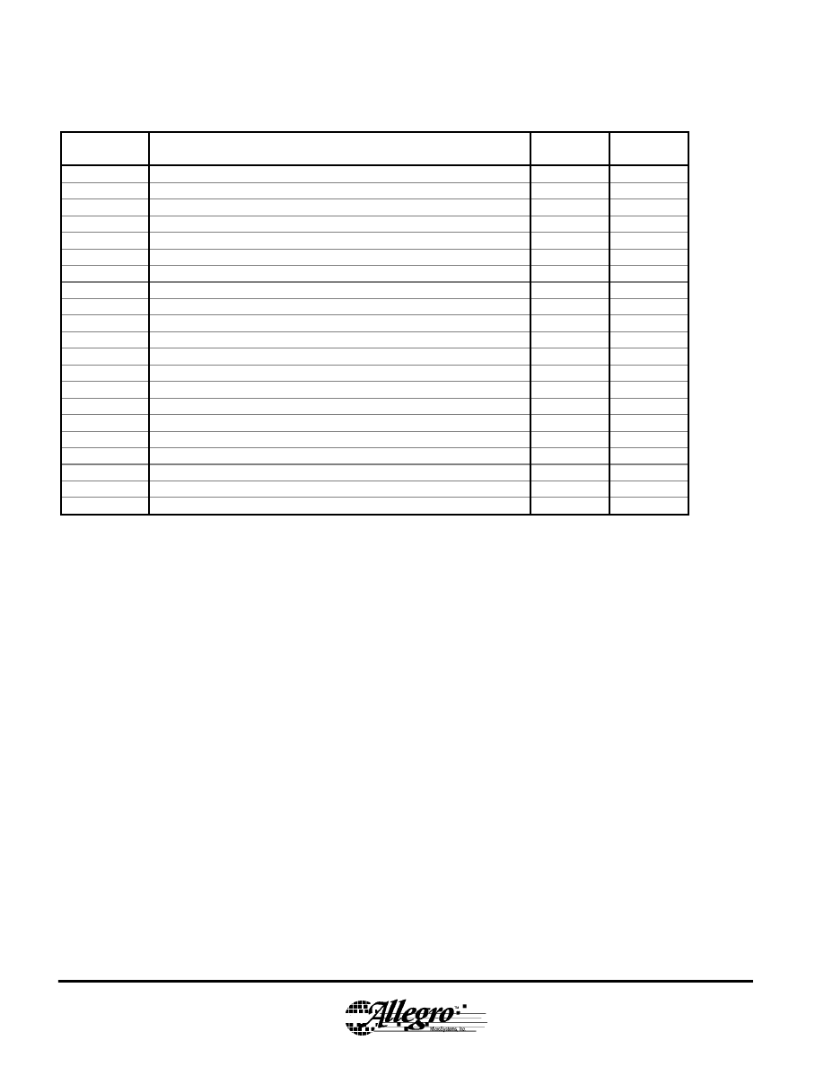
8281/8282
Pin Name
Pin Description
8281SLB
SO-16
8282SLB
SO-24
EXTM
External modulation input
1
24
OLF
Overload flag output
2
2
VBULK
Tracking supply voltage to linear regulators
3
3
GND
Ground tab
4
6,7
SENSE
Current limit setup resistor
5
8
LNB
Output voltage to LNB
6
9
LX
Inductor drive point
7
10
VIN
Supply input voltage
8
11
TCAP
Capacitor for setting the rise and fall time of the outputs
9
12
LLC
Logic input: increases output voltage by 1 V for line length
-
13
VSEL1
Logic input: output voltage select
10
14
VSEL0
Logic input: output voltage select
-
15
EN
Logic input: enables switcher and outputs
11
16
ENT
Logic input: enable internal modulation
12
17
GND
Ground tabs
13
18,19
CPUMP
High side of charge-pump cap
14
20
VPUMP
Gate supply voltage for high side drivers
15
21
PUMPX
Charge-pump drive
16
22
VINT
Internal regulated supply
-
23
N/C
No Connect
1,4,5
Document Outline
Wyszukiwarka
Podobne podstrony:
1 4 11id 8282
8282
8282, W2- budownictwa
8282
8282
8282
8282
8282
8282
8282
8282
8282
8282 02 Latin exam 2006
więcej podobnych podstron