
Graphene-Based Liquid Crystal Device
Peter Blake,
†
Paul D. Brimicombe,
‡
Rahul R. Nair,
‡
Tim J. Booth,
§
Da Jiang,
|
Fred Schedin,
|
Leonid A. Ponomarenko,
‡
Sergey V. Morozov,
⊥
Helen F. Gleeson,
‡
Ernie W. Hill,
†
Andre K. Geim,
|
and Kostya S. Novoselov*
,‡
School of Computer Science, UniVersity of Manchester,
Manchester M13 9PL, United Kingdom, School of Physics & Astronomy, UniVersity of
Manchester, Manchester M13 9PL, United Kingdom, Graphene Industries Limited,
32 Holden AVenue, Whalley Range, Manchester M16 8TA, United Kingdom,
Centre for Mesoscience and Nanotechnology, UniVersity of Manchester,
Manchester M13 9PL, United Kingdom, and Institute for Microelectronics Technology,
142432 ChernogoloVka, Russia
Received March 4, 2008; Revised Manuscript Received April 8, 2008
ABSTRACT
Graphene is only one atom thick, optically transparent, chemically inert, and an excellent conductor. These properties seem to make this
material an excellent candidate for applications in various photonic devices that require conducting but transparent thin films. In this letter,
we demonstrate liquid crystal devices with electrodes made of graphene that show excellent performance with a high contrast ratio. We also
discuss the advantages of graphene compared to conventionally used metal oxides in terms of low resistivity, high transparency and chemical
stability.
Graphene is the first example of truly two-dimensional
materials.
1
Only one atom thick, it demonstrates high
crystallographic quality
2
and ballistic electron transport on
the micrometer scale.
1
Such unique properties make it a
realistic candidate for a number of electronic applications.
In particular, graphene is an attractive material for optoelec-
tronic devices, in which its high optical transmittance, low
resistivity, high chemical stability, and mechanical strength
seems to make it an ideal optically transparent conductor.
Transparent conductors are an essential part of many
optical devices. Traditionally, thin metallic or metal oxide
films are used for these purposes (for a review see ref 3). At
the same time, there is a constant search for new types of
conductive thin films, as existing technologies are often
complicated (e.g., thin metallic films require antireflection
coating
3
) and expensive (often using noble or rare metals).
Furthermore, many of the widely used metal oxides exhibit
nonuniform absorption across the visible spectrum
4
and are
chemically unstable (for instance, the commonly used indium
tin oxide (ITO, In
2
O
3
:Sn) is known to inject oxygen
5
and
indium
6
ions into the active media of a device). Recently
carbon nanotube films have been produced
7
and used as an
alternative transparent conductor in various photonic devices
including electric-field-activated optical modulators,
7
organic
solar cells,
8
and liquid crystal displays.
9
The experimental
discovery of graphene
10
brought a new alternative to the
ubiquitous ITO. The optical properties of this material are
now being widely tested,
11–15
and graphene films have
recently been used as transparent electrodes for solar cells.
16
In this letter, we report on the use of graphene as a
transparent conductive coating for photonic devices and show
that its high transparency and low resistivity make this two-
dimensional crystal ideally suitable for electrodes in liquid
crystal devices. We will also argue that graphene, being
mechanically strong, chemically stable, and inert, should
improve the durability and simplify the technology of
potential optoelectronic devices.
Graphene flakes were prepared by micromechanical cleav-
age
10,17
on a glass microscope slide. They were first located
using an optical microscope
18
(Figure 1f,g) and then further
identified as monolayer graphene using Raman microscopy.
19
Thin (55 nm) chromium/gold contacts were then deposited
around the flakes, so the graphene crystal was effectively
covering a window in the metallization, Figure 1a,b (this
geometry also eliminates stray electric fields from the edges
of the electrode). Planar-aligned liquid crystal devices were
then fabricated using such graphene-on-glass films as one
of the transparent electrodes, Figure 1a. The other substrate
was of a glass slide coated with conventional ITO. Both
substrates were coated with a polyvinyl alcohol alignment
* Corresponding author. E-mail: kostya@manchester.ac.uk. Telephone:
+44-(0)161-275-41-19. Fax:+44-(0)161-275-40-56.
†
School of Computer Science, University of Manchester.
‡
School of Physics & Astronomy, University of Manchester.
§
Graphene Industries Limited.
|
Centre for Mesoscience and Nanotechnology, University of Manchester.
⊥
Institute for Microelectronics Technology.
NANO
LETTERS
2008
Vol. 8, No. 6
1704-1708
10.1021/nl080649i CCC: $40.75
2008 American Chemical Society
Published on Web 04/30/2008
Downloaded by UNIV MANCHESTER on July 10, 2009
Published on April 30, 2008 on http://pubs.acs.org | doi: 10.1021/nl080649i
layer that was subsequently baked and then unidirectionally
rubbed (ITO-coated substrate only) in order to promote
uniform alignment of the liquid crystal director. The device
was then capillary-filled with nematic liquid crystal material
E7 (Merck). Applying a voltage across the liquid crystal layer
distorts the crystal alignment, changing the effective bire-
fringence of the device and altering the transmitted light
intensity.
20
A control sample, with an opening in the
metallization not covered by graphene, was also prepared
(Figure 1h). Note that, although we will limit our consid-
eration of graphene-based liquid crystal devices to those with
planar untwisted nematic liquid crystals, this technology
could equally be applied to any of the various nematic liquid
crystal device types (e.g., twisted nematic,
21
supertwisted
nematic,
22
in-plane switching,
23
and vertically aligned ne-
matic
24
devices) and also to ferroelectric and other liquid
crystal devices that use smectic phases.
An ac (square-wave) voltage was applied across the cells
in order to reorient the liquid crystal director. The electro-
optic properties were observed using an optical microscope
with the device placed between crossed polarizers and the
rubbing direction oriented 45
°
with respect to the polarizers.
Above the expected threshold voltage of around 0.9 Vrms,
a strong change in the transmission is observed (Figures
1b-e, 2) both in white and monochromatic light. The fact
that the whole electrode area changes contrast uniformly
suggests that the electric field is applied uniformly through
the area of graphene and that the graphene has no negative
effect on the liquid crystal alignment. The contrast ratio
(between maximum transmission and the transmission when
100 Vrms is applied across the cell) is better than 100 under
illumination using white light, which is very good for this
type of cell and demonstrates that graphene could indeed be
used effectively as a transparent electrode for liquid crystal
displays. No significant changes in transmission were
observed for the control sample, with only edge effects
appearing due to the finite thickness of the cell, Figure 1h.
We will now assess the quality of our liquid crystal
devices, concentrating on such important issues as the
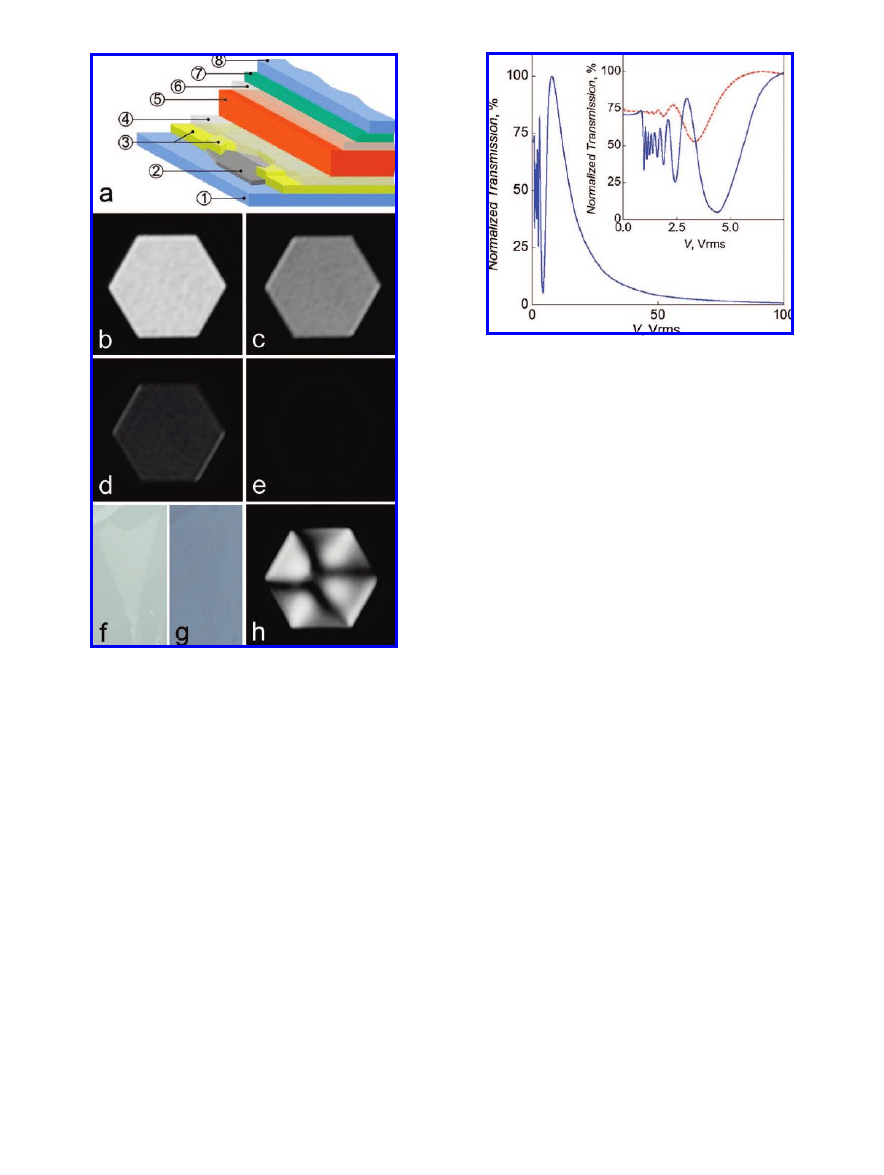
Figure 1
.
(a) Schematic diagram of our liquid crystal devices with
typical layer thicknesses in brackets: 1, glass (1 mm); 2, graphene;
3, Cr/Au contact surrounding graphene flake (5 nm Cr + 50 nm
Au); 4, alignment layer (polyvinyl alcohol) (40 nm); 5, liquid crystal
(20
µm); 6, alignment layer (40 nm); 7, ITO (150 nm); 8, glass (1
mm). The graphene flake is surrounded by a nontransparent Cr/Au
contact. (b-e) Optical micrographs of one of our liquid crystal
devices using green light (505 nm, fwhm 23 nm) with different
voltages applied across the cell: (b) V ) 8 Vrms; (c) V ) 13 Vrms;
(d) V ) 22 Vrms; (e) V ) 100 Vrms. Overall image width is 30
µm. The central hexagonal window is covered by graphene,
surrounded by the opaque Cr/Au electrode. (f) An optical micro-
graph (in reflection, using white light) of a graphene flake on the
surface of a 1 mm thickness glass slide. The contrast is of the order
of 6%. Overall image width is 10
µm. (g) The same image but in
transmission. The flake is practically invisible. (h) Control device
with no graphene in the opening of the Cr/Au contacts with V )
100 Vrms applied across the cell. Because the electrode on the
ITO-coated surface is continuous, there is a significant stray field
within the window that distorts the liquid crystal structure, leading
to the pattern shown.
Figure 2
.
Light transmission through the liquid crystal device as a
function of voltage applied across the cell, normalized to the
maximum transmission. Inset: the same at low voltages. Solid blue
curve: in green light, 505 nm, fwhm 23 nm; dashed red curve: in
white light. The data taken in white light practically coincide with
those in green light for voltages above 10 Vrms and are omitted
from the main panel for clarity. From the oscillatory behavior the
thickness of the liquid crystal layer is estimated to be
∼20 µm,
assuming that the birefringence of E7 is 0.225.
Nano Lett., Vol. 8, No. 6, 2008
1705
Downloaded by UNIV MANCHESTER on July 10, 2009
Published on April 30, 2008 on http://pubs.acs.org | doi: 10.1021/nl080649i
transparency of graphene, its resistivity, and chemical
stability. Light absorption by this two-dimensional material
has been studied on suspended mono- and few-layer graphene
flakes. In such samples, graphene covers an aperture (about
30
µm in diameter) in metallic foil so that light transmission
could be measured directly (further details can be found in
ref 15). The results are presented in Figure 3 (right inset) as
a function of the number of layers. Each layer of graphene
absorbs about 2%, which is significantly lower than that of
conventionally used ITO (15-18%
3
).
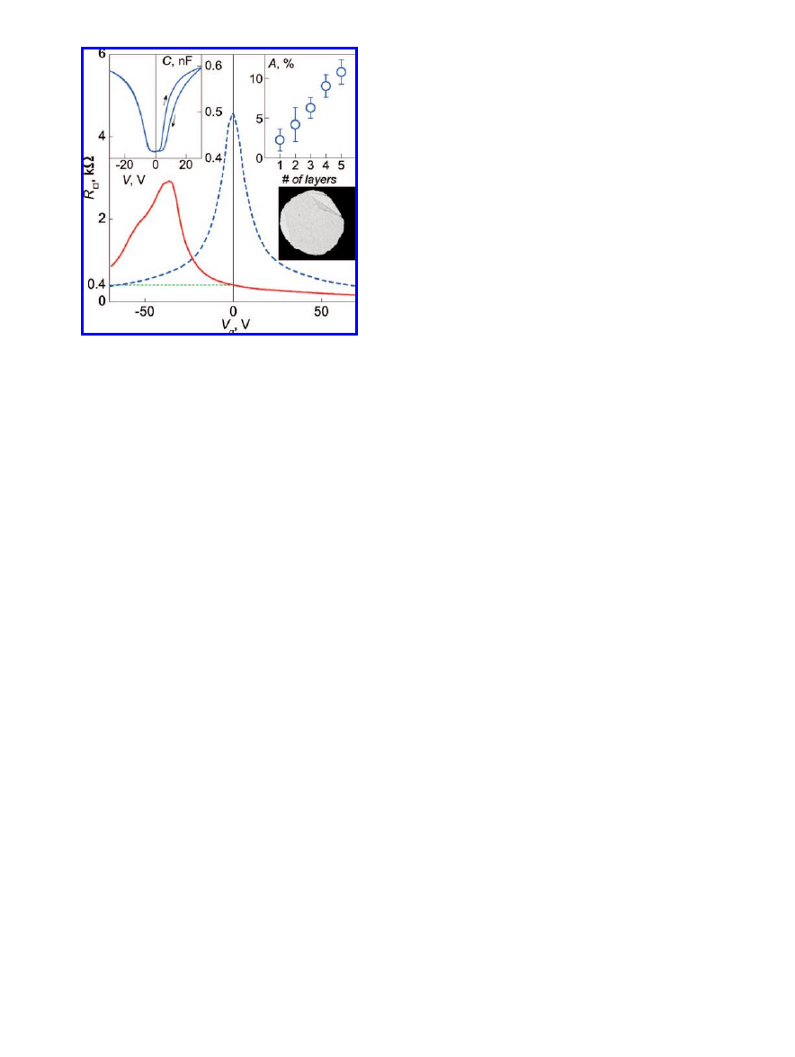
The sheet resistance of undoped graphene is of the order
of 6 k
Ω (one conductivity quantum per species of charge
carriers
1
). However, it can be reduced down to 50
Ω by
chemical doping,
10,25
and even unintentional doping (due to
molecules absorbed from the surrounding atmosphere, e.g.,
water)
10
can be of the order of 10
12
cm
-2
. In liquid crystal
devices, an electrode is usually in direct contact with an
alignment layer (in our case polyvinyl alcohol). We have
tested the doping of graphene with polyvinyl alcohol by
preparing a standard graphene device on a 300 nm SiO
2
/Si
wafer and measuring its gate response with and without a
layer of polyvinyl alcohol on top of graphene (Figure 3).
The introduction of a layer of polyvinyl alcohol produces
n-type doping of about 3
× 10
12
cm
-2
. For this particular
sample, it resulted in a drop in the sheet resistance down to
400
Ω, which is an impressive result for a conductive coating
with optical transmission of about 98%. It is difficult to
compare this result to ITO, as the resistance of In
2
O
3
:Sn films
diverges strongly (on the order of tens of k
Ω) when trying
to obtain optical transmittance above 95%. ITO films with
95% transmittance demonstrate comparable sheet resistances
of a few hundred Ohms, dropping to tens of Ohms at an
optical transmittance of about 90%.
26
Similar or even lower
resistances can be achieved for graphene by a variety of
means: increasing the number of layers,
27
intentional doping,
or by using samples with higher mobility.
28,29
It is evident
from Figure 3 (right inset) that even five layers of graphene
absorb only
≈10% of light, which is well inside the
industrially relevant limit.
An important issue for most ITO-based liquid crystal
devices and other photonic devices is the chemical stability
of the metal oxide and the diffusion of ions into the active
media. Such processes deteriorate the active media (for
example via oxidation if oxygen is injected
5
) and can lead
to breakdown at lower voltages. Furthermore, in liquid crystal
displays, the injected ions get trapped at the alignment layer,
thus screening the applied electric field. This leads to the
so-called image sticking problem,
30
which is usually avoided
by driving the liquid crystal cells with alternating voltage.
One can generally expect that such issues can be avoided
when using graphene, where its chemical stability should
minimize the level of ion diffusion. To check this, we have
measured the capacitance of one of our liquid crystal devices,
which has one electrode made of graphene and the other
from ITO, when applying dc voltages of different polarities
(Figure 3 left inset, here positive voltage corresponds to
higher potential on the ITO electrode). There is clearly a
highly hysteretic response when applying positive biases,
but no hysteresis has been observed at the opposite
polarity. We attribute this observation to positive indium
ions drifting into the liquid crystal from the ITO electrode,
whereas no ions are injected from the graphene electrode.
Similar liquid crystal devices constructed using ITO elec-
trodes on both substrates produce the hysteretic response for
both polarities.
Although it is important to demonstrate the possibility and
advantages of using graphene as a transparent conductive
coating, the feasibility of its mass production is essential
when considering realistic applications. No industrial tech-
nology can rely on the micromechanical cleavage technique
that allows only minute quantities of graphene and, although
sufficient for fundamental research and proof-of-concept
devices, is unlikely to become commercially viable. Recently,
large-area conductive films have been demonstrated by using
chemical exfoliation of graphite oxide and then reducing it
to graphene.
16,31,32
This could lead to a viable way of making
thin graphene-based films with properties similar to those
discussed earlier and using them for various photonic devices.
However, so far this technique has not demonstrated the
ability to fully recover the excellent conductive properties
of graphene.
33
We propose an alternative approach. It
involves making a graphene suspension by direct chemical
exfoliation of graphite (rather than graphite oxide), which
is subsequently used to obtain transparent conductive films
on top of glass by spin- or spray-coating.
Figure 3
.
Sheet resistance of a graphene device as a function of
gate voltage with (solid red curve) and without (dashed blue curve)
a layer of polyvinyl alcohol on top. Polyvinyl alcohol provides
n-type doping, shifting the curve to negative gate voltages. The
sheet resistance at zero gate voltage is
∼400 Ω. Left inset:
capacitance of one of our liquid crystal devices as a function of
voltage applied. Right inset: light absorption of suspended graphene
of different thicknesses. The bottom picture represents a TEM
micrograph of a 30
µm aperture covered by suspended graphene
used in these experiments. Light absorption by graphene could be
measured as a contrast between the area covered by the material
and the empty space: there is a gap on the left and folded area (top
right). Similar suspended structures of few-layer graphene has been
prepared and studied in the experiment.
1706
Nano Lett., Vol. 8, No. 6, 2008
Downloaded by UNIV MANCHESTER on July 10, 2009
Published on April 30, 2008 on http://pubs.acs.org | doi: 10.1021/nl080649i
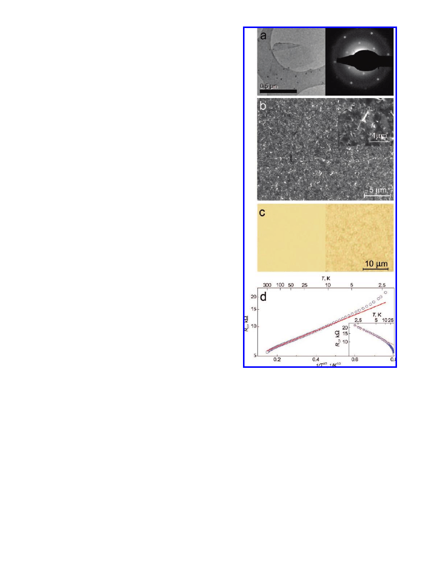
Crystals of natural graphite (Branwell Graphite Ltd.) were
exfoliated by sonication in dimethylformamide (DMF) for
over 3 h. DMF “dissolves” graphite surprisingly well, and
the procedure resulted in a suspension of thin graphitic
platelets with large proportion of monolayer graphene flakes,
DMF also wets the flakes preventing them from conglom-
erating.
34
The suspension was then centrifuged at 13000 rpm
for 10 min to remove thick flakes. The remaining suspension
consists mostly of graphene and few-layer graphite flakes
of submicrometer size. The thickness of the exfoliated flakes
has been verified by atomic force microscopy and transmis-
sion electron microscopy (Figure 4a). Both techniques
indicate high proportion of monolayer flakes (up to 50%).
The suspension was spray-deposited onto a preheated glass
slide (Figure 4b,c) that yielded thin (
∼1.5 nm) films over
centimeter sized areas, which consisted of overlapping
individual graphene and few-layer graphene flakes. These
films were then annealed for 2 h in argon(90%)/hydro-
gen(10%) atmosphere at 250
°
C. The transparency of these
graphitic layers was approximately 90% (Figure 4c), which
is expected for 4-5 layers of graphene coverage (Figure 3,
right inset) and is still well within the margins of being
relevant for industrial applications.
To measure the resistivity of our films, a mesa structure
in the shape of the Hall bar with typical dimensions of 1
mm was prepared, and the four-probe resistance was
measured as a function of temperature (Figure 4d). The high
temperature region (above 10 K) is well described by exp(T
0
/
T
1/3
) dependence, characteristic for variable range hopping
in two dimensions.
35
The room temperature sheet resistance
is of the order of 5 k
Ω, which, together with the high
transparency of 90%, is already acceptable for some ap-
plications
3,16
and can be decreased further by increasing the
film thickness. Resistance at low temperatures deviates from
the variable-range-hopping dependence but can be described
by the simple activation dependence exp(-
∆/T) (see inset
in Figure 4d). We attribute this low-temperature behavior
to weak tunneling-like coupling between overlapping flakes,
possibly due to contamination with organic (DMF) residues.
The procedure we used can also modify the chemical
termination of the dangling bonds of our graphene crystal-
lites, which might affect the transport properties of the films
obtained (although on a lesser level than the contamination
between the overlapping flakes). This indicates some poten-
tial for improvements as better cleaning and annealing
procedures may improve the coupling between graphene
crystallites and decrease the film resistance further.
To conclude, high optical transparency, low resistivity,
and high chemical stability of graphene makes it an
excellent choice for transparent electrodes in various
optoelectronic devices. Furthermore, there are already
several technologies that potentially allow mass production
of thin graphene-based transparent conductors (besides the
chemical exfoliation of graphite described in the present
letter, one can also think of epitaxial growth of graphene
on top of a metal surface, followed by a transfer of such
a layer onto a transparent substrate
1
). These techniques are
capable of producing continuous graphene films of thickness
below five monolayers, which is required for realistic
applications.
Acknowledgment. The authors are grateful to EPSRC for
financial support. A.K.G. and K.S.N. also acknowledge
support from the Royal Society, UK. S.V.M. thanks RFBR
for financial support.
Figure 4
.
(a) TEM image (left panel) and electron diffraction pattern
(right pannel) of a graphene flake obtained by the chemical
exfoliation method. Equal intensity of first- and second-order
diffraction peaks confirms that the flake is exactly one monolayer
thick. (b) Scanning electron micrograph of a thin graphitic film
obtained by chemical exfoliation and spray-coating. Inset shows
the same area under higher magnification. (c) Light transmission
through an original glass slide (left) and the one covered with the
graphitic film (right). (d) Temperature dependence of the film’s
sheet resistance (R
∼ exp(T
0
/T
1/3
) behavior is observed at T > 10
K, where T
0
is a constant
35
). Inset: the same data but for the low
temperature interval (R
∼ exp(∆/T) behavior is observed at T < 10
K, where
∆ is a constant). The red lines are guides for the eye.
Nano Lett., Vol. 8, No. 6, 2008
1707
Downloaded by UNIV MANCHESTER on July 10, 2009
Published on April 30, 2008 on http://pubs.acs.org | doi: 10.1021/nl080649i
References
(1) Geim, A. K.; Novoselov, K. S. Nat. Mater. 2007, 6, 183
.
(2) Meyer, J. C.; Geim, A. K.; Katsnelson, M. I.; Novoselov, K. S.; Booth,
T. J.; Roth, S. Nature 2007, 446, 60
.
(3) Granqvist, C. G. Sol. Energy Mater. Sol. Cells 2007, 91, 1529
.
(4) Phillips, J. M.; Kwo, J.; Thomas, G. A.; Carter, S. A.; Cava, R. J.;
Hou, S. Y.; Krajewski, J. J.; Marshall, J. H.; Peck, W. F.; Rapkine,
D. H.; van Dover, R. B. Appl. Phys. Lett. 1994, 65, 115
.
(5) Scott, J. C.; Kaufman, J. H.; Brock, P. J.; DiPietro, R.; Salem, J.;
Goitia, J. A. J. Appl. Phys. 1996, 79, 2745
.
(6) Schlatmann, A. R.; Wilms Floet, D.; Hilberer, A.; Garten, F.; Smulders,
P. J. M.; Klapwijk, T. M.; Hadziioannou, G. Appl. Phys. Lett. 1996,
69, 1764
.
(7) Wu, Z. C.; Chen, Z. H.; Du, X.; Logan, J. M.; Sippel, J.; Nikolou,
M.; Kamaras, K.; Reynolds, J. R.; Tanner, D. B.; Hebard, A. F.;
Rinzler, A. G. Science 2004, 305, 1273
.
(8) van de Lagemaat, J.; Barnes, T. M.; Rumbles, G.; Shaheen, S. E.;
Coutts, T. J.; Weeks, C.; Levitsky, I.; Peltola, J.; Glatkowski, P. Appl.
Phys. Lett. 2006, 88, 233503
.
(9) Chan Yu King, R.; Roussel, F. Appl. Phys. A: Mater. Sci. Process.
2007, 86, 159
.
(10) Novoselov, K. S.; Geim, A. K.; Morozov, S. V.; Jiang, D.; Zhang,
Y.; Dubonos, S. V.; Grigorieva, I. V.; Firsov, A. A. Science 2004,
306, 666
.
(11) Blake, P.; Hill, E. W.; Castro Neto, A. H.; Novoselov, K. S.; Jiang,
D.; Yang, R.; Booth, T. J.; Geim, A. K. Appl. Phys. Lett. 2007, 91,
063124
.
(12) Abergel, D. S. L.; Russell, A. I.; Fal’ko, V. Appl. Phys. Lett. 2007,
91, 063125
.
(13) Casiraghi, C.; Hartschuh, A.; Lidorikis, E.; Qian, H.; Harutyunyan,
H.; Gokus, T.; Novoselov, K. S.; Ferrari, A. C. Nano Lett. 2007, 7,
2711
.
(14) Kuzmenko, A. B.; van Heumen, E.; Carbone, F.; van der Marel, D.
Phys. ReV. Lett. 2008, 100, 117401
.
(15) Nair, R. R.; Blake, P.; Grigorenko, A. N.; Novoselov, K. S.; Booth,
T. J.; Stauber, T.; Peres, N. M. R.; Geim, A. K. Science 2008,
published online 3 April 2008;, DOI: 10.1126/science.1156965
.
(16) Wang, X.; Zhi, L.; Mullen, K. Nano Lett. 2008, 8, 323
.
(17) Novoselov, K. S.; Jiang, D.; Schedin, F.; Booth, T.; Khotkevich, V. V.;
Morozov, S. V.; Geim, A. K. Proc. Natl. Acad. Sci. U.S.A. 2005, 102,
10451
.
(18) Graphene flakes on glass are feebly visible in reflection, giving rise
to about 6% contrast (confirmed by both experiment and theoretical
modeling, similar to ref 11)
.
(19) Ferrari, A. C.; Meyer, J. C.; Scardaci, V.; Casiraghi, C.; Lazzeri, M.;
Mauri, F.; Piscanec, S.; Jiang, D.; Novoselov, K. S.; Roth, S.; Geim,
A. K. Phys. ReV. Lett. 2006, 97, 187401
.
(20) Fre´edericksz, V.; Zolina, V. Trans. Faraday Soc. 1933, 29, 919
.
(21) Schadt, M.; Helfrich, W. Appl. Phys. Lett. 1971, 18, 127
.
(22) Watters, C. M.; Brimmell, V.; Raynes, E. P. Proceedings of the 3rd
International Display Research Conference, Kobe, Japan, 1983, p 396
.
(23) Soref, R. A. J. Appl. Phys. 1974, 12, 5466
.
(24) Schiekel, M. F.; Fahrenchon, K. Appl. Phys. Lett. 1971, 19, 391
.
(25) Schedin, F.; Geim, A. K.; Morozov, S. V.; Hill, E. W.; Blake, P.;
Katsnelson, M. I.; Novoselov, K. S. Nat. Mater. 2007, 6, 652
.
(26) Sheet resistance of ITO films diverges strongly with decreasing its
thickness. See for example. Wong, F. L.; Fung, M. K.; Tong, S. W.;
Lee, C. S.; Lee, S. T. Thin Solid Films 2004, 466, 225
.
(27) Morozov, S. V.; Novoselov, K. S.; Schedin, F.; Jiang, D.; Firsov, A. A.;
Geim, A. K. Phys. ReV. B 2005, 72, 201401(R)
(28) The sample shown in Figure 3 exhibits a mobility of about 0.5 m
2
/
V·s. Graphene samples with room-temperature mobility as high as 2
m
2
/V·s have been obtained by micromechanical cleavage.
(29) Morozov, S. V.; Novoselov, K. S.; Katsnelson, M. I.; Schedin, F.;
Elias, D. C.; Jaszczak, J. A.; Geim, A. K. Phys. ReV. Lett. 2008, 100,
016602
.
(30) Bremer, M.; Naemura, S.; Tarumi, K. Jpn. J. Appl. Phys. 1998, 37,
L88
.
(31) Stankovich, S.; Dikin, D. A.; Dommett, G. H. B.; Kohlhaas, K. M.;
Zimney, E. J.; Stach, E. A.; Piner, R. D.; Nguyen, S. T.; Ruoff, R. S.
Nature 2006, 442, 282
.
(32) Li, D.; Mu¨ller, M. B.; Gilje, S.; Kaner, R. B.; Wallace, G. G. Nat.
Nanotechnol. 2008, 3, 101
.
(33) Gomez-Navarro, C.; Weitz, R. T.; Bittner, A. M.; Scolari, M.; Mews,
A.; Burghard, M.; Kern, K. Nano Lett. 2007, 7, 3499
.
(34) Hernandez, Y.; Nicolosi, V.; Blighe, F. M.; Sun, Zh.; Gun’ko, Yu.;
Hutchison, J.; Scardaci, V.; Ferrari, A. C.; Coleman, J. N. Nat.
Nanotechnol. Submitted for publication.
(35) Mott, N. F. Phil. Mag. 1969, 19, 835
.
NL080649I
1708
Nano Lett., Vol. 8, No. 6, 2008
Downloaded by UNIV MANCHESTER on July 10, 2009
Published on April 30, 2008 on http://pubs.acs.org | doi: 10.1021/nl080649i
Wyszukiwarka
Podobne podstrony:
15 Nature Nano 3 210 215 2008id Nieznany (2)
12 Nano Lett 8 2442 2446 2008id Nieznany (2)
21 Nano Lett 8 173 177 2008id 29096
cw 16 odpowiedzi do pytan id 1 Nieznany
16 ROZ w sprawie warunkow tec Nieznany
9 16 12 2011 grammaire descrip Nieznany (2)
5 16 marca 2011 Morfologia grz Nieznany
16 2 Transport ko owyid 16731 Nieznany
16 Przygotowanie pasieki do zim Nieznany (2)
16 Burze i pioruny 2id 16899 Nieznany (2)
16 pr%b9dy indukowane%5bfeynman Nieznany (2)
16 ROZ warunki tech uzytkow Nieznany (2)
16 Doustne postacie lekow o mod Nieznany (2)
11 Phys Rev B 78 085432 2008id Nieznany (2)
pdfviewer vid=16&hid=101&sid=c6 Nieznany
k1e sb14 16 2015 2016 KOL1e inf Nieznany
16 dostosowanie zakladu do obow Nieznany (2)
PMP 16 10 10 id 363483 Nieznany
więcej podobnych podstron