Parameter
DC Input Voltage
Output Current
Power Dissipation
*
Junction Temperature
Storage Temperature
Thermal Resistance (Junction to Case)
Thermal Resistance (Junction to Ambient Air)
Symbol
V
IN
I
O
P
D
T
j
T
stg
R
th(j-c)
R
th(j-a)
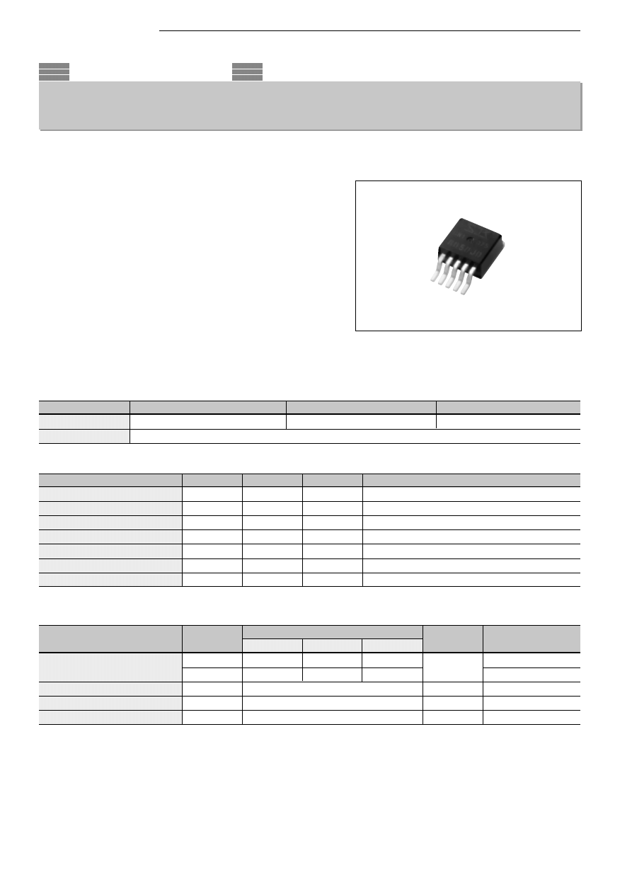
SI-8000JD Series
Surface-Mount, Separate Excitation Switching Type
●
SI-8000JD Series
Conditions
I
O
=0 to 1A
I
O
=0 to 1.5A
V
IN
≥
V
O
+3V
Symbol
V
IN1
V
IN2
I
O
T
jop
T
op
■
Absolute Maximum Ratings
■
Recommended Operating Conditions
Unit
V
A
W
°
C
°
C
°
C/W
°
C/W
Part Namber
SI-8033JD
SI-8050JD
SI-8090JD
V
O
(V)
3.3
5.0
9.0
I
O
(A)
1.5
Ratings
43
1.5
3
+125
–40 to +125
3
33.3
Ratings
SI-8033JD
SI-8050JD
SI-8090JD
5.3 to 6.3
7 to 8
11 to 12
6.3 to 40
8 to 40
12 to 40
0 to 1.5
–30 to +125
–30 to +125
Conditions
Glass-epoxy board mounting 40
×
40 mm (copper area 100%)
Glass-epoxy board mounting 40
×
40 mm (copper area 100%)
Unit
V
A
°
C
°
C
Parameter
DC Input Voltage Range
DC Output Current Range
*
Operating Junction Temperature Range
Operating Temperature Range*
*: Limited by Ta–P
D
characteristics
*: Limited by thermal protection circuit
■
Features
• Surface-mount package (TO263-5)
• Output current: 1.5 A
• High efficiency: 77 to 86%
• Requires only 4 external components
• Phase correction and output voltage adjustment performed internally
• Choke coil size can be reduced through the employment of high frequency
(125 kHz) design
• Built-in foldback overcurrent protection, thermal protection circuit
• Output ON/OFF possible (OFF state current consumption: 200
µ
A max)
• Soft start possible via ON/OFF pin
■
Applications
• Power supplies for telecommunication equipment
• Onboard local power supplies, etc.
■
Lineup
●
SI-8000JD Series
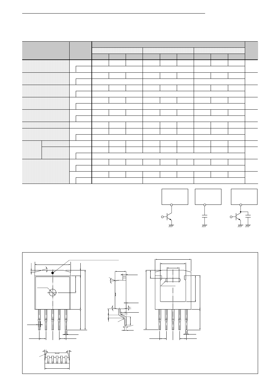
■
External Dimensions
(Unit : mm)
Pin Arrangement
q
V
IN
w
SW
OUT
e
GND
r
V
OS
t
ON/OFF
Plastic Mold Package Type
Flammability: 94V-0
Weight: Approx. 1.48g
Parameter
Output Voltage
Efficiency
Switching Frequency
Line Regulation
Load Regulation
Temperature Coefficient of Output Voltage
Overcurrent Protection
Starting Current
ON/OFF
*
Low Level Voltage
Pin
Low-State
Output Current
Quiescent Circuit Current
■
Electrical Characteristics
(T
a
=25
°
C)
Unit
V
%
kH
Z
mV
mV
mV/
°
C
A
V
µ
A
mA
µ
A
Symbol
V
O
Conditions
η
Conditions
f
Conditions
∆
V
OLINE
Conditions
∆
V
OLOAD
Conditions
∆
V
O
/
∆
T
a
I
S1
Conditions
V
SSL
I
SSL
Conditions
I
q
Conditions
I
q(oFF)
Conditions
*: Pin 5 is the ON/OFF pin. Connecting a capacitor to this pin enables a soft
start at power-on. By using this pin, the output can also be turned on or off.
By setting the voltage of this pin to V
SSL
or lower, the output is stopped.
Driving a transistor with an open collector can perform switching of the po-
tential of the ON/OFF pin.
When using both the soft-start and ON/OFF functions together, the
discharge current from C3 flows to the ON/OFF control transistor, so
ensure that this current is limited for protection. The ON/OFF pin is pulled
up to the power supply in the IC, so no external voltage can be applied. If
this pin is not used, leave it open.
SI-8000JD
SI-8000JD
ON/OFF
5
ON/OFF
5
ON/OFF
C3
C3
5
V
OUT.
ON/OFF
Soft Start
Soft Start
+V
OUT.
ON/OFF
SI-8000JD
(0.40)
15.30
±
0.3
(6.8)
9.2
±
0.2
4.9
±
0.2
2.54
±
0.3
(4.6)
9.2
±
±
0.2
1.2
±
0.2
4.9
±
0.2
(0.75)
2.0
±
0.1
(1.75)
15.3
±
0.3
9.90
±
0.2
Case Temperature Measurement Point
(15
°
)
(0.5)
2-R0.3
10.0
±
0.02
3-R0.3
(2
×
R0.45)
(R0.3)
(R0.3)
0.88
±
0.10
1.5 Dp:
±
0.2
φ
(1.7
±
0.25
)
1
2
3
4
5
(1.7
±
0.25
)
(1.7
±
0.25
)
(1.7
±
0.25
)
0.8
±
0.1
0.8
±
0.1
4.5
±
0.2
1.3
0.10
±
0.15
2.4
±
0.2
+0.10
–0.05
10.0
±
0.2
(4.4)
(8.0)
(3
°
)
(3
°
)
(3
°
)
(3
°
)
(3
°
)
0~6
°
Ratings
SI-8033JD
SI-8050JD
SI-8090JD
min.
typ.
max.
min.
typ.
max.
min.
typ.
max.
3.234
3.30
3.366
4.90
5.00
5.10
8.82
9.00
9.18
V
IN
=15V, I
O
=0.5A
V
IN
=20V, I
O
=0.5A
V
IN
=21V, I
O
=0.5A
77
82
86
V
IN
=15V, I
O
=0.5A
V
IN
=20V, I
O
=0.5A
V
IN
=21V, I
O
=0.5A
125
125
125
V
IN
=15V, I
O
=0.5A
V
IN
=20V, I
O
=0.5A
V
IN
=21V, I
O
=0.5A
25
80
40
100
50
120
V
IN
=8 to 30V, I
O
=0.5A
V
IN
=10 to 30V, I
O
=0.5A
V
IN
=15 to 30V, I
O
=0.5A
10
30
10
40
10
40
V
IN
=15V, I
O
=0.2 to 0.8A
V
IN
=20V, I
O
=0.2 to 0.8A
V
IN
=21V, I
O
=0.2 to 0.8A
±
0.5
±
0.5
±
1.0
1.6
1.6
1.6
V
IN
=15V
V
IN
=20V
V
IN
=21V
0.5
0.5
0.5
100
100
100
V
SSL
=0V
7
7
7
V
IN
=15V, Io=0A
V
IN
=20V, Io=0A
V
IN
=21V, Io=0A
200
200
200
V
IN
=15V, V
ON/OFF
=0.3V
V
IN
=20V, V
ON/OFF
=0.3V
V
IN
=21V, V
ON/OFF
=0.3V
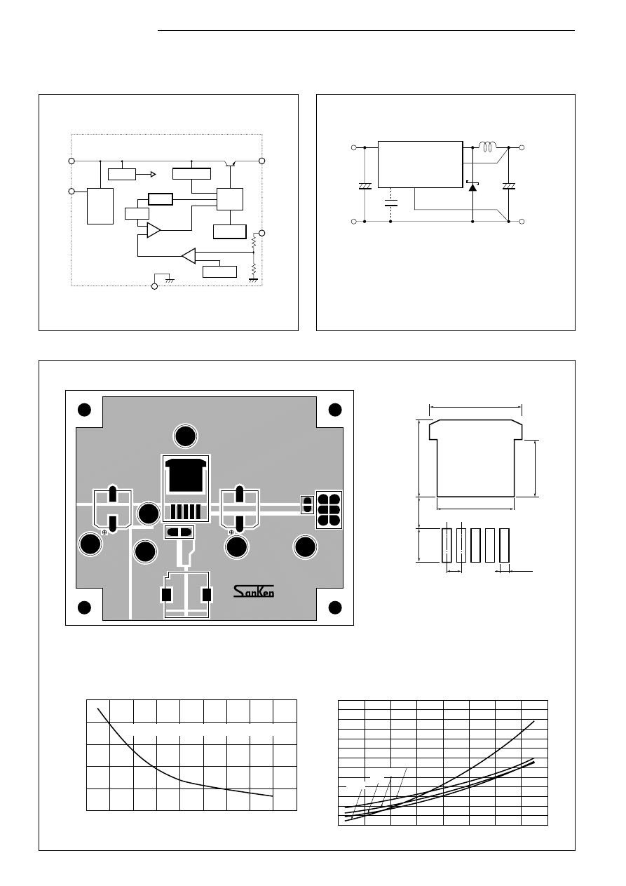
■
Example of Pattern on PC Board
* For the optimum operating conditions, use one-point GND wiring centering on pin 3, and place each component as closely as
possible.
●
SI-8000JD Series
■
Block Diagram
■
Standard External Circuit
Area of Copper on Glass Epoxy Board vs.
Thermal Resistance (Junction to Ambient Air) (Typical Value)
4
3
GND
2
V
IN
ON/OFF
SW OUT
1
5
PReg.
OCP
Reset
OSC
+
–
Comp.
Error Amp.
Latch &
Drive
TSD
ON/OFF
Soft
Start
V
REF
+
–
V
IN
C
1
C
3
Di
L1
C
2
V
IN
GND
ON/OFF
GND
SI-8000JD
SW
V
S
1
2
4
3
5
+
+
V
OUT
GND
C
1 :
50V/220
µ
F
C
2 :
25V/470
µ
F
C
3 :
10V/0.47
µ
F (when using soft-start function)
L
1 :
100
µ
H
Di
:
SFPB-66 (Sanken)
C
1
C
2
C
3
SI-8000JD
GND
GND
S
Vins
Vos
Vout
Di
Di
Vin
SW
SI- 8 0 0 0 JD
6.8
±
0.1
9
±
0.2
3.7
±
0.05
4
±
0.1
11
±
0.2
9
±
0.1
1.7
±
0.1
1
±
0.05
Unit : mm
55
50
45
40
35
30
2.6
2.4
2.2
2.0
1.8
1.6
1.4
1.2
1.0
0.8
0.6
0.4
0.2
0
0
200
0
0.2
0.4
0.6
0.8
1.0
1.2
1.4
1.6
400
600
800
1000
Copper area (mm
2
)
Output Current I
O
(A)
V
IN
8V
20V
30V
40V
Thermal Resistance (junction to ambient air)
j-a (
°
C/W )
Power Dissipation
Pd (W)
1200
1400
1600
1800
With glass epoxy board measuring 40
×
40 mm
θ
Recommended Pattern
Recommended Land Pattern
Output Current vs. Power Dissipation (Typical)
■
T
a
-P
D
Characteristics
The efficiency depends on the input voltage and the
output current. Therefore, obtain the value from the
efficiency characteristic curve and substitute the per-
centage in the formula above.
V
O
: Output Voltage
V
IN
: Input Voltage
I
O
: Output Current
ηχ
: Efficiency (%)
V
F
: D
1
forward voltage
0.4V(I
O
=2A)(SFPB-66)
Thermal design for D
1
must be done separately.
3.5
3
2.5
2
1.5
1
0.5
0
–25
0
25
50
75
100
125
Power Dissipation P
D
(W)
Ambient Temperature T
a
(
°
C)
Copper Area
40
×
40 mm
( j-a : 33.3
°
C/W)
20
×
40 mm
( j-a : 37
°
C/W)
20
×
20 mm
( j-a :44
°
C/W)
10
×
10 mm
( j-a : 53
°
C/W)
θ
θ
θ
θ
●
SI-8000JD Series
P
D
=V
O
• I
O
100
–1
–V
F
• I
O
1–
V
O
ηχ
V
IN
■
Selecting External Components
1. Inductor L
1
q
It must be suitable for a switching regulator.
Do not use inductors such as for noise filters, because they generate excessive heat.
w
The rated current must be satisfied.
If the rated current is exceeded, magnetic saturation leads to overcurrent.
2. Capacitor C
1
, C
2
q
The breakdown voltage and allowable ripple current must be satisfied.
Exceeding the ratings of these capacitors or using them without derating shortens their service lives and may also cause abnormal
oscillation of the IC.
w
Use a low-impedance type capacitor for C
2
.
C
2
must be a low-impedance type capacitor to ensure reduced ripple voltage and a stable switching operation.
e
Do not use a capacitor that has an extremely small ESR (equivalent series resistance) such as an OS capacitor or tantalum capacitor.
r
C
3
is a capacitor for soft start. When not using soft start, leave pin 5 open. It is pulled up inside the IC.
3. Diode D
1
The Sanken SFPB-66 diode is recommended for D1. If you intended to use an equivalent diode, be sure to use a Schottkey Barrier diode.
If you use a fast recovery diode or any other diode, supplying a reverse voltage generated from the recovery or ON voltage of the diode
may damage the IC.
Application
Variable output voltage
Output voltage can be adjusted in the same way as SI-8000S.
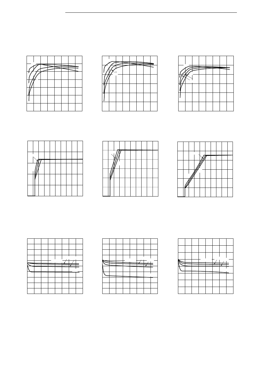
Efficiency Characteristics
(SI-8033JD)
(SI-8050JD)
(SI-8090JD)
Output Voltage Characteristics
(SI-8033JD)
(SI-8050JD)
(SI-8090JD)
Load Regulation (SI-8033JD)
(SI-8050JD)
(SI-8090JD)
■
Typical Characteristics
90
80
70
60
50
40
30
20
0
0.2
0.4
0.6
0.8
1.0
1.2
1.4
1.6
Output Current I
O
(A)
(T
a
=25
°
C)
V
IN
=6.3V
15V
30V
40V
Efficiency (%)
η
5
4
3
2
1
0
0
2
6
10
14
18
4
8
12
Input Voltage V
IN
(V)
Output Voltage V
O
(V)
16
20
(Load=C.R T
a
=25
°
C)
1.5A
I
O
=0A
0.5A
3.40
3.38
3.36
3.34
3.32
3.30
3.28
3.26
3.24
3.22
3.20
15V
30V
6.3V
Output Voltage V
O
(V)
0
0.2
0.4
0.6
0.8
1.0
1.2
1.4
1.6
Output Current I
O
(A)
(T
a
=25
°
C)
V
IN
=40V
90
80
70
60
50
40
30
0
0.2
0.4
0.6
0.8
1.0
1.2
1.4
1.6
Output Current I
O
(A)
(T
a
=25
°
C)
V
IN
=8V
20V
40V
30V
Efficiency (%)
η
6
5
4
3
2
1
0
0
2
6
10
14
18
4
8
12
Input Voltage V
IN
(V)
0.5A
Output Voltage V
O
(V)
16
20
(Load=C.R T
a
=25
°
C)
I
O
=0A
1.5A
5.10
5.08
5.06
5.04
5.02
5.00
4.98
4.96
4.94
4.92
4.90
20V
8V
Output Voltage V
O
(V)
0
0.2
0.4
0.6
0.8
1.0
1.2
1.4
1.6
Output Current I
O
(A)
(T
a
=25
°
C)
V
IN
=40V
30V
100
90
80
70
60
50
40
Efficiency (%)
0
0.2
0.4
0.6
0.8
1.0
1.2
1.4
1.6
Output Current I
O
(A)
(T
a
=25
°
C)
V
IN
=12V
40
V
21V
30V
η
12
10
8
6
4
2
0
0
2
6
10
14
18
4
8
12
Input Voltage V
IN
(V)
Output Voltage V
O
(V)
16
20
(T
a
=25
°
C)
1.5A
I
O
=0A
0.5A
9.20
9.15
9.10
9.05
9.00
8.95
8.90
8.85
8.80
21V
12V
Output Voltage V
O
(V)
0
0.2
0.4
0.6
0.8
1.0
1.2
1.4
1.6
Output Current I
O
(A)
(T
a
=25
°
C)
V
IN
=40V
30V
●
SI-8000JD Series
Overcurrent Protection Characteristics
(SI-8033JD)
(SI-8050JD)
(SI-8090JD)
Thermal Protection Characteristics
(SI-8033JD)
(SI-8050JD)
(SI-8090JD)
Temperature Characteristics
(SI-8033JD)
(SI-8050JD)
(SI-8090JD)
Output Voltage V
O
(V)
5
4
3
2
1
0
0
0.5
1.0
Output Current I
O
(A)
1.5
2.0
2.5
3.0
(T
a
=25
°
C)
V
IN
=8V
15V
30V
40V
50
75
100
125
150
175
200
5
4
3
2
1
0
Ambient Temperature T
a
(
°
C)
Output Voltage V
O
(V)
V
IN
=15V, I
O
=0A
TSD OFF
TSD ON
150
140
130
120
110
100
90
80
70
60
Output Voltage V
O
(V)
–40 –20
0
20
40
60
80
100 120 140
Ambient Temperature T
a
(
°
C)
Freq
3.38
3.36
3.34
3.32
3.30
3.28
3.26
3.24
3.22
3.20
η
V
O
V
IN
=15V, I
O
=0.5A
Efficiency (%) Operating Frequency (kHz)
η
Output Voltage V
O
(V)
6
5
4
3
2
1
0
0
0.5
1.0
Output Current I
O
(A)
1.5
2.0
2.5
3.0
(T
a
=25
°
C)
V
IN
=10V
20V
30V
40V
150
140
130
120
110
100
90
80
70
60
Output Voltage V
O
(V)
–40 –20
0
20
40
60
80
100 120 140
Ambient Temperature T
a
(
°
C)
Freq
5.08
5.06
5.04
5.02
5.00
4.98
4.96
4.94
4.92
4.90
V
O
V
IN
=20V, I
O
=0.5A
η
Efficiency (%) Operating Frequency (kHz)
η
Output Voltage V
O
(V)
12
10
8
6
4
2
0
0
0.5
1.0
Output Current I
O
(A)
1.5
2.0
2.5
3.0
(T
a
=25
°
C)
V
IN
=40V
30V
21V
14V
150
140
130
120
110
100
90
80
70
60
Output Voltage V
O
(V)
–40 –20
0
20
40
60
80
100 120 140
Ambient Temperature T
a
(
°
C)
Freq
9.10
9.08
9.06
9.04
9.02
9.00
8.98
8.96
8.94
8.92
V
O
V
IN
=21V, I
O
=0.5A
η
Efficiency (%) Operating Frequency (kHz)
η
50
75
100
125
150
175
200
10
8
6
4
2
0
Ambient Temperature T
a
(
°
C)
Output Voltage V
O
(V)
V
IN
=20V, I
O
=0A
TSD OFF
TSD ON
50
75
100
125
150
175
200
10
8
6
4
2
0
Ambient Temperature T
a
(
°
C)
Output Voltage V
O
(V)
V
IN
=21V, I
O
=0A
TSD OFF
TSD ON
●
SI-8000JD Series
[Note on Thermal Protection]
The thermal protection circuit is intended for protection against
heat during instantaneous short-circuiting. Its operation is not
guaranteed for continuous heating conditions such as short-cir-
cuiting over extended periods of time.
Wyszukiwarka
Podobne podstrony:
Adsorption of active ingredients of surface disinfectants depends on the type
SI wstep
SI Slowniczek VIsem
SI – Sensory Integration
wyk5 si
Palec bozy SI id 798905 Nieznany
druk szkody kl si
OWU SI OiPT 08 07
Epidemiologia SI, Epidemiologia
Metoda SI - notatka, metodyka pracy korekcyjno kompensacyjnej
ZP Reszta pyta ktre si nie powtrzyy
SI LAB4
8 zasilanie odbiorcow uklady si Nieznany (2)
Metody efektywnego uczenia si i pisania prac projektowych
islamzachod si
Jak dobieramy si w pary Paprzycka Mianowska Izdebski
Czowiek ktry min si z Chrystusem
Pos ugiwanie si miernikami elektrycznymi
OWU SI NNW 08 07
więcej podobnych podstron