1 2
SPARC
Applications
by Richard Pedreau
1 8
Caller ID Fundamentals
by Richard Newman
2 2
Vehicular Control Multiplexing with CAN and
Part 1: Vehicular Multiplexing Fundamentals
by Willard Dickerson
2 8
The Embedded Sun
Part 1: Introduction to the Hardware
by Anindya Ray Lee Hanson
DSP in RISC Embedded Processors
by Richard Pedreau
Fujitsu’s
Alternatives
by
Burns
3 8
Embedding a Message-based System
by Pat Baird
q
From the Bench
Finally Fill the Rainbow
Bachiochi
S e e
9 0
q
Silicon Update
Fuzzy PID-Pong
Tom Can
Political Arachnids
Letters to the Editor
New Product News
edited by
Weiner
Circuit Cellar INK@
Issue
April 1996

FREEDOM OF SPEECH
Steve’s INK 67 editorial reminded me of the astute-
ness of a
I saw recently: “Law is not always just,
and justice is not always legal.”
Since this issue went to press, I’m sure you’ve heard
the brouhaha over the book Hit Man. I’m not in favor of
murder for hire. But, I am incensed that some would
deny me the right to obtain the knowledge of how to do
it! Right now, the author is a pariah because his book
was seemingly used as instruction for an actual murder.
But, if circumstances were different..
for in-
stance, that a foreign power took over our government
and the book was used for a successful assassination of
the usurpers; the author would be a hero.
Context is all. My right to know should not be taken
away just because someone used that knowledge to do
evil.
I was surfing the Internet the other day and managed
to land on a Web page sponsored by legitimate,
to-God (pardon the pun) Satanists. I investigated, and
when I found out that it was too wickedly serious for
my taste and sensibilities, you know what I did? I re-
fused to investigate further, got out, and left it behind.
In my opinion, that was censorship at its finest.
Heck, I’m not even an elderly grandmother, and what I
saw shocked me (but I do have breasts). I defined it as
obscene. I had the freedom of choice and I exercised it,
as I do every day.
You are so right that “unless we collectively head off
the dim-witted thinking that government intervention
and censorship are tools to preserve a free society, we
are destined to lose a society and freedom worth pre-
serving.” I can decide for myself, thank you, and I can
train up my children (well, he is grown now, but I did
my best) in the way they should go. I don’t need Big
Brother’s help.
Too bad I have to go to work and am rushed or I
could have written you a letter worthy of another edito-
rial. I just wanted you to know that “It Just Frosts My
Chops” was greatly appreciated.
Pat Shields
via the Internet
TO LETTERS
I would like to reply to a letter in
67 from Jim
Chaney regarding the Engine-Control System series
62-64).
Mr. Chaney wrote, “Although Ed’s two-coil ignition
system is fine for drag racing, for a street application,
the increased plug wear over a four-coil system would
be unacceptable. There’s a need for a feedback of resis-
tance at the spark plugs during various
and load,
which should also provide cylinder pressure calcula-
tions.”
Buick has been using a distributorless ignition sys-
tem with two cylinders per coil since the mid ’80s.
Spark plug wear was actually less in my Buick GN
(turbocharged
than previous cars with traditional
distributors. Now, practically all manufacturers use a
similar system.
About measuring plug resistance, Chrysler uses a
two-coil DIS system in the four-cylinder Neon. With
the advent of
regulations, monitoring the plug
resistance was required for misfire detection. The waste
spark system has a negligible amount of resistance from
the plug not under load. So, total secondary resistance is
dominated by the actively firing (compression stroke)
plug. The waste spark helps emissions, as the extra
spark on the exhaust stroke can ignite the remaining
hydrocarbons.
Keep up the good work, INK!
Dave Cooley
Wendell, NC
Contacting Circuit Cellar
We at Circuit Cellar
communication be-
tween our readers and our staff, have made every effort to
make contacting us easy. We prefer electronic communications,
but feel free to use any of the following:
Mail: Letters to the Editor may be sent to: Editor, Circuit Cellar INK,
4 Park St., Vernon, CT 06066.
Phone: Direct all subscription inquiries to (800)
Contact our editorial offices at (860) 8752199.
Fax: All faxes may be sent to (860)
BBS: All of our editors and regular authors frequent the Circuit
Cellar BBS and are available to answer questions. Call
(860) 871-1988 with your modem
bps,
Internet: Letters to the editor may be sent to
corn. Send new subscription orders, renewals, and ad-
dress changes to
Be sure to
include your complete mailing address and return E-mail
address in all correspondence. Author E-mail addresses
(when available) may be found at the end of each article.
For more information, send E-mail to
corn.
WWW: Point your browser to
FTP: Files are available at
6
Issue
April 1996
Circuit Cellar INK@
Edited by Harv Weiner
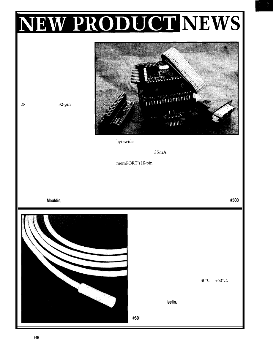
ADD-ON SERIAL PORT FOR SBC
memPORT provides that extra
serial port so often needed for debug-
ging single-board computers during
program development or on site.
Prior to memPORT, developers had
to temporarily relinquish a port or
build an extra port into every prod-
uct.
The 2” x 1.8” memPORT PC board
is installed through an adapter into a
or 32-pin DIP or
PLCC
memory socket. It contains a buff-
ered UART, RS-232 level conversion,
memory-mapping logic, and a DIP
memory-replacement socket.
Through the replacement socket, the
system continues to use the dis-
placed memory IC, except for a small block of eight
addresses.
In return, the system gains a memory-mapped RS-232 serial port with full-duplex operation at up to 115.2 kbps,
double-buffer transmit, and a quadruple-buffer receive. Power, typically
over and above that needed by the
memory IC, is taken from the memory socket.
A flat cable assembly makes the transition from
header to an AT-compatible DE-9 connector.
Software guidelines are included for setting up the UART and for typical polled transfer routines. If the user’s soft-
ware-development program can’t be customized, the port can be used for the application itself.
memPORT comes complete with transition cable for $139. Memory socket adapters are available as a DIP for $25
or as an economy PLCC version for $30.
Rhombus
P.O. Box 871
l
SC 29662
l
(803) 676-0012
l
Fax: (803) 676-0015
LOW-TEMPERATURE SENSOR
The M2020 NTC Thermistor replaces traditional
electromechanical devices with an electronic component
that provides more sensitive temperature regulation.
When the M2020 is used with a microprocessor inter-
face, actual temperatures can be displayed. The sensor
was designed specifically for refrigerators and freezers.
Encapsulated in a molded plastic case, the M2020
withstands harsh temperature conditions. Under test
conditions of 1,000 h at room temperature in water, the
change in the resistance value is less than 1%. The
M2020 also achieves fast temperature cycling. At tem-
peratures changing 100 times from
to
the
change in resistance is less than 1%.
Siemens Components, Inc.
186 Wood Ave. S.
l
NJ 08830
(908) 906-4300
l
Fax: (908) 632-2830
8
Issue
April 1996
Circuit Cellar INK@
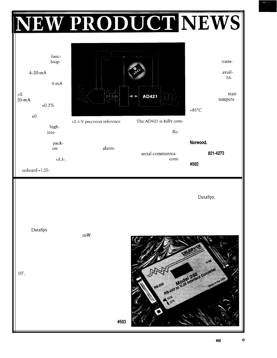
LOW-COST DAC
To control a variety of
digital communication
digital-processing
with intelligent field
tions, the AD421
instruments and
powered D/A converter
mitters.
sends
signals to
The AD421 is
a microcontroller. It
able in 16-pin DIP,
offers a zero-scale
lead SOIC, and 16-lead
output current with
SSOP packages. The part
1% offset error and a
is specified over the
full-scale output
dard industrial
current with
gain
ture range of -40°C to
error. Full-scale settling
and costs $6.95 in
time to
1% occurs
quantity.
within 5 ms.
The DAC is a
voltages. The device also
patible with the standard
Analog Devices, Inc.
precision, fully
features a high-speed
Highway Addressable
One Technology Way
grated, low-cost solution
2-Mbps serial interface, a
mote Transducer (HART)
P.O. Box 9106
housed in a 16-pin
clock oscillator circuit, and
protocol or other similar
MA 02062-9106
age. It includes an
a programmable
Frequency Shift Keying
(617) 329-4700
board voltage regulator
current capability which
(FSK)
Fax: (617)
which provides +5-,
lets the transmitter send
tions methods. This
or +3-V outputs as well
out-of-range currents to
munication protocol allows
as
and
indicate a transducer fault.
simultaneous analog and
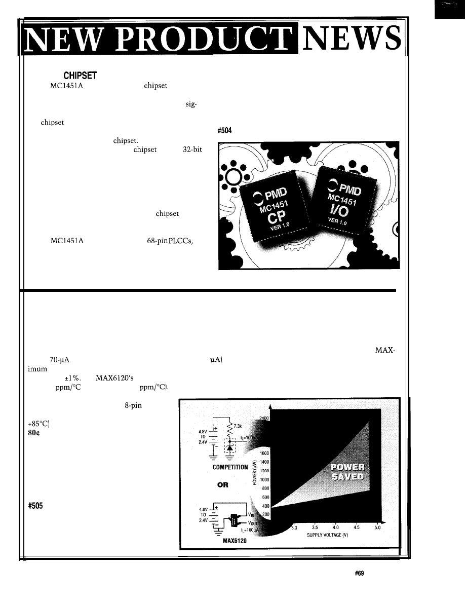
RS-232-TO-V.35 CONVERTER
The Model 240 Universal RS-232-to-V.35 Interface Converter efficiently steals power from the RS-232 interface
and provides a DTE- or DCE-switchable configuration. It includes a unique LCD display, called
that in-
forms the user of the status of the data and handshake signals included in the RS-232 interface.
Supporting data rates that range from DC to 100 kbps, Model 240 includes conversion circuitry for 13 signals. The
power to drive the unit is derived from the interface signals (data, control, and clocks) on the RS-232 port. At a mini-
mum, TD and one control signal are required. The Model 240 incorporates an externally accessible switch to config-
ure the unit as a DTE or DCE device.
The
LCD display provides status information about the interface signals being processed by the con-
verter. It operates from less than 1
of power and
does not affect the operation of the Model 240. The
graphic display presents the user with live status of the
transmit and receive data signals (TD and RD) and con-
trol signals (CTS, RTS, DSR, DCD, and DTR).
The electrical interface for both ports is implemented
in DB-25 female connectors. Each unit is supplied with a
male-to-male DB-25 extension cable which can be
used on either the RS-232 or V.35 port. Additional cables
are available.
Model 240 is packaged in a rugged metal case measur-
ing 3.3” x 2.86” x 0.76” and sells for $220.
Telebyte Technology, Inc.
270 Pulaski Rd.
Greenlawn, NY 11740-1616
(516) 423-3232
l
Fax: (516) 385-8184
Circuit Cellar INK@
Issue
April 1996
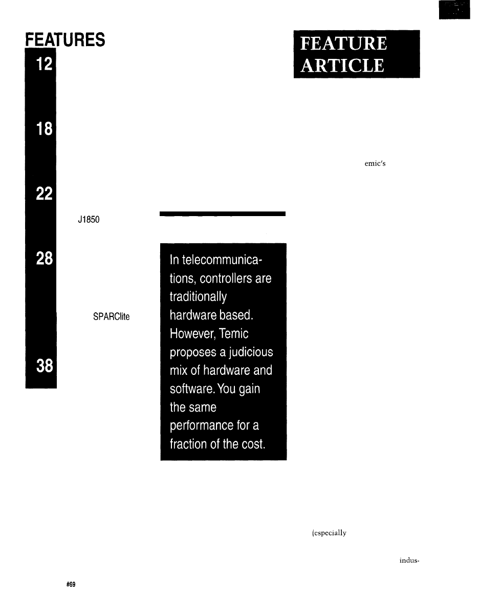
STEPPER
The
intelligent-motion
supports up
Performance Motion Devices, Inc.
to
four axes of electronic gearing. The master input for
97 Lowell Rd.
each axis is provided by quadrature encoder input
Concord, MA 01742
nals. The output consists of pulse and direction signals.
(508) 369-3302
l
Fax: (508) 369-3819
The
is programmed using any standard micropro-
cessor by sending high-level motion instructions which
are then interpreted by the
Other standard features of the
include
motion registers, programmable breakpoints, host inter-
rupts, and three user-selectable profiling modes: S-curve,
trapezoidal, and velocity contouring.
In addition, a special motor-stall-detection capability
has been added. This feature uses the encoder feedback
signal to determine when the motor has lost steps, even
while the motor is in motion. When the
detects a
stall condition, it safely shuts down the ongoing move to
avoid system damage.
The
is packaged in two
with
an optional 44-pin PLCC used for encoder feedback.
Pricing for the four-axis version with encoder feedback is
$129 in quantity.
PRECISION, THREE-TERMINAL REFERENCE
Maxim Integrated Products has released the MAX1620, the first 1.2-V micropower, precision three-terminal volt-
age reference offered in an SOT-23 package. Ideal for 3-V battery-powered equipment where power conservation is
critical, the MAX1620 is a low-power alternative to existing two-terminal shunt references.
Unlike two-terminal references that throw away battery current and require an external series resistor, the
1620’s
maximum supply current (typically only 42
is independent of the input voltage, which means max
efficiency at all battery voltages. In addition, it operates from a supply voltage as low as 2.4 V, and initial
accuracy is
The
temperature drift is 100% tested in the SOT-23 package and guaranteed to be less
that 100
(typically only 50
The MAX1620 is available in a 3-pin
SOT-23 package, as well as an
SO
package in the extended-industrial (-40°C to
temperature range. Prices start at
(1000s).
Maxim integrated Products
120 San Gabriel Dr.
Sunnyvale, CA 94086
(408) 737-7600
Fax: (408) 737-7194
Circuit Cellar INK@
Issue
April 1996
11
SPARC Telco
Applications
SPARC
Telco
Applications
Caller ID Fundamentals
Vehicular Control
Multiplexing with CAN
and
The Embedded Sun
DSP in RISC Embedded
Processors
Fujitsu’s
Alternatives
Embedding a
Message-based System
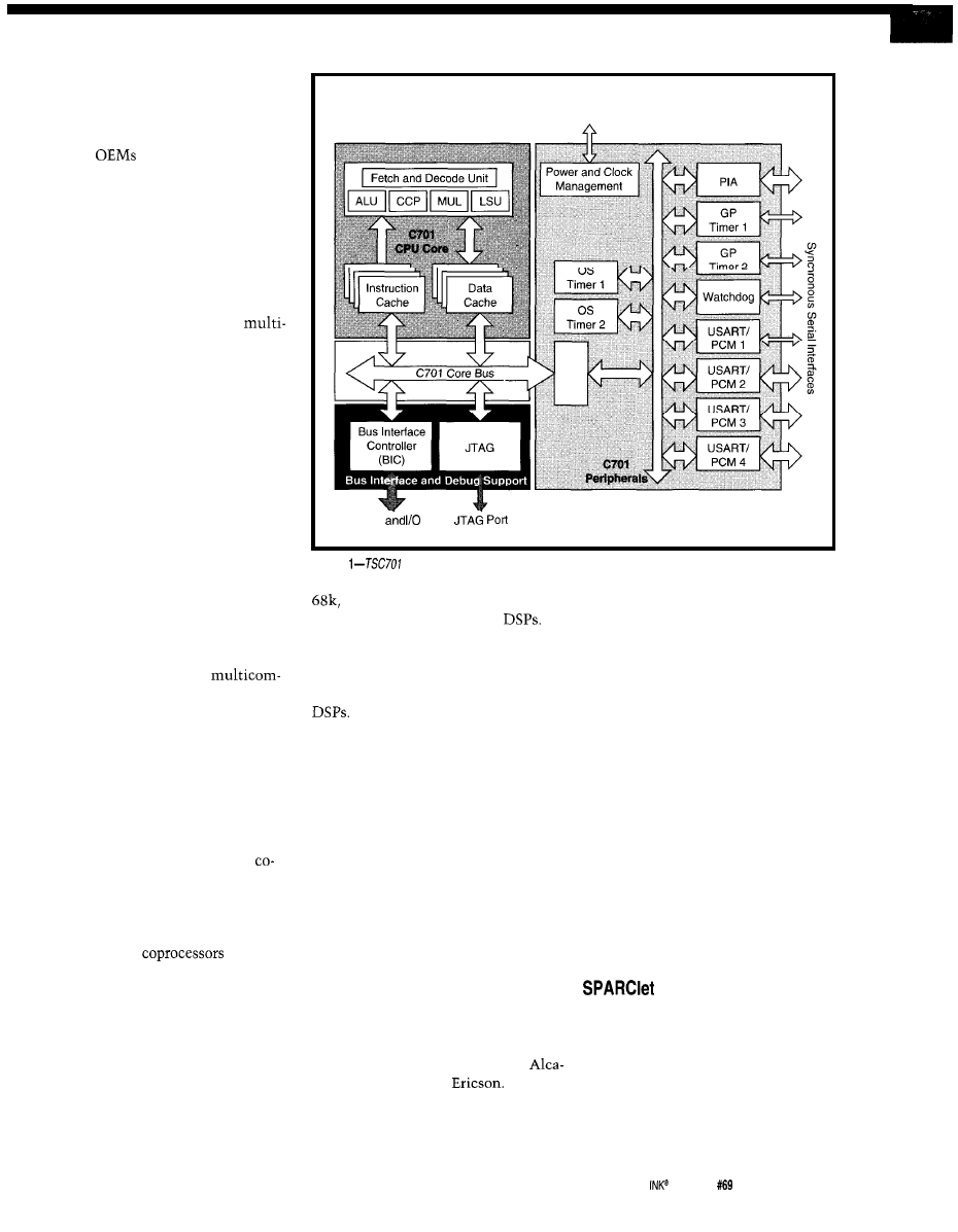
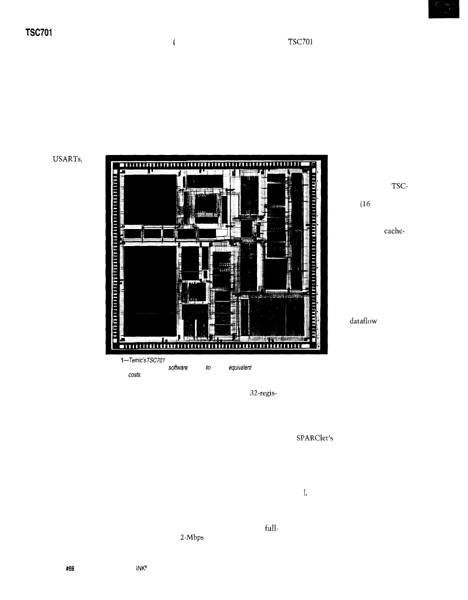
Richard Pedreau
0
TSC701
Advanced Commu-
nication Controller,
pictured in Photo
1,
ini-
tiates a new challenge in embedded
telecommunication applications. This
innovative concept is built on three
premises: increased flexibility, com-
bined online signal processing and
protocol handling, and maintaining
performance at the system level.
New multistandards (e.g., for base
stations or handsets), proprietary pro-
tocols, and rapid product evolution
bring with them the need for increased
flexibility which outperforms the
usual hardware-based solutions. A
software approach, to the extent that it
reaches the same overall performance
level, brings much more flexibility.
Emerging communication applica-
tions need signal-processing features
(e.g., compression capability) com-
bined with real-time protocol handling
and the usual control skills on a single
chip. The ideal is to include only the
necessary DSP functions, thus achiev-
ing the best performance-to-cost ratio
from a component standpoint.
The performance-to-cost ratio ex-
tends to the system level. Subsequent-
ly, the challenge is to preserve the
performance level at the highest level
while using low-cost peripherals like
PC-type DRAM.
MULTISTANDARDS
The new telecommunication stan-
dards or multistandards originate in
part from local regulatory organiza-
tions
in Europe) which
force different rules from one country
to the next. Because telecom equip-
ment manufacturers are usually
12
Issue
April 1996
Circuit Cellar INK@
try giants, the advantages of a flexible
approach-keeping the customization
operation as late as possible in the
process-are obvious.
Most
want to start with
globally usable hardware (including
wireless base stations, PABX, ISDN
adaptors, and even telephone sets) and
simply customize it with different
line-interface daughterboards and soft-
ware. This approach reduces manufac-
turing costs while improving overall
quality.
A second reason for the new
standards is the need to adapt the same
equipment to different uses. An obvi-
ous example is the telephone handset.
The handset is slowly evolving to
become a personal piece of equipment
and not a community one. From one
phone at home, one wireless, and one
portable, the trend is toward one hand-
set per individual, which can function
both in GSM/PCN (portable] mode and
DECT (wireless) mode for home or
office.
This emerging general-purpose
wireless handset must remain low cost
while becoming at least five times
more capable. In this area, these chal-
lenges pend:
l
size constraints prohibit
ponent solutions
l
the silicon-area enlargement required
for a comprehensive processor with
full DSP implementation leads to an
unacceptable cost increase for con-
sumer electronics
Since a processor needs to control
the equipment, it makes most sense to
integrate chosen DSP features as
processors in a powerful but physically
small RISC core.
Thus, the large computing power of
the RISC CPU enables it to handle the
integrated DSP
as another
execution unit. Basic equipment man-
agement uses only about 10% of its
CPU load, which is perhaps the only
way such a versatile handset can be
conceived.
This approach brings DSP functions
back to where they left off over 10
years ago. Then, the lack of computing
power in the main processor core of
the CISC processors at the time of the
Clock and
Reset
Memory
Bus
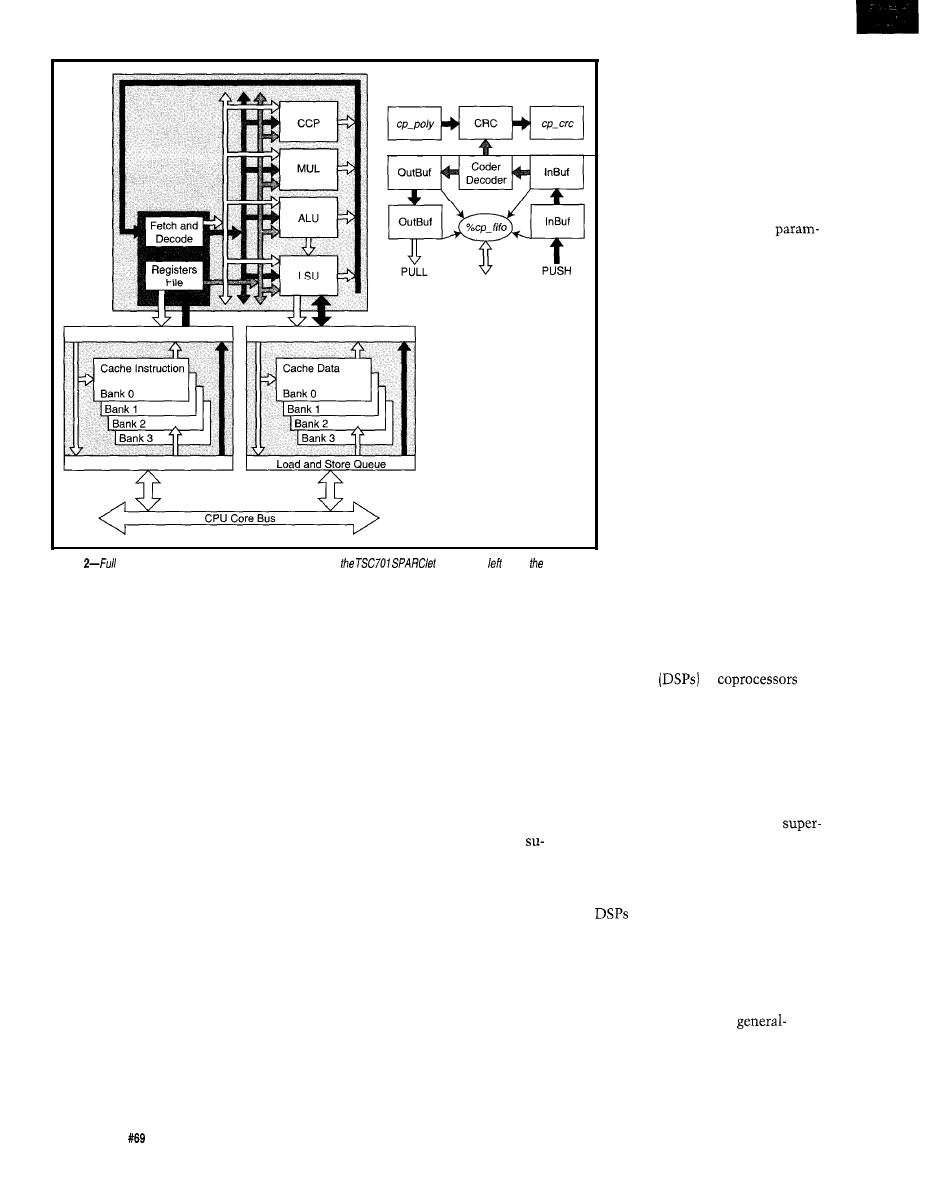
Figure
combines online signal processing and protocol handling.
28000, and similar processors
paved the way for specialized
I don’t mean to imply that DSP
processors will become obsolete. On
the leading edge of technology, there’s
always a place for high-end specialized
They’re the only way to solve
certain calculation problems. But,
CPU architectures can usually come
back a few years later with a “normal-
ized” solution.
To enlarge the scope of this discus-
sion, the tendency to actually integrate
so-called “visual” instructions into the
new processors (like Sun or Intel) is
another example of the same evolu-
tion. Although until now this field has
been restricted to highly specialized
processors, in my opinion it will soon
return to the standard processor area.
PROPRIETARY PROTOCOLS
Proprietary protocols are the norm
in this field. Communications is an
area where one finds very important
multinational companies such as
tel, Nortel, Nokia, or
These
companies logically have to preserve
their know-how by using proprietary
protocols. On the other hand, they
must also remain close to the standard
to preserve the industry compatibility.
In dealing with proprietary proto-
cols, there are some very practical
advantages to a software approach like
Temic’s TSC701. First, this approach
makes it easy to respond to slight
variations in protocol parameters like
CRC polynom, recognition flags, chan-
nel filtering, and so on.
Also, competitive software solu-
tions should come with a comprehen-
sive library of drivers in documented
source format as well as directly im-
plementable binary files.
Thus, the user has two advantages:
fast time to market using a provided
turnkey solution, and the ability to
later customize the drivers to react to
application upgrades.
ARCHITECTURAL
CONCEPT
The TSC701, whose components
are diagrammed in Figure 1, combines
online signal processing and protocol
handling.
As a principle, SPARClet maxi-
mizes use of all hardware resources
when it’s logically possible to do so.
Circuit Cellar
Issue
April 1996
13
Figure
message coding and sending is accomplished by
core on the
using
process
outlined on the right.
The first target, however, is not perfor-
mance, but rather price to perfor-
mance. In particular, resources are not
duplicated to increase performance
[i.e., it’s not a superscalar design].
A resource (e.g., the adder) is used
as soon as it is free and the operands
are available. There are two reasons for
an instruction to stall. The first is data
dependency.
The other reason an instruction can
stall is resource dependency. Resourc-
es for most instructions are available
every cycle. However, this is not al-
ways true.
Because we want to proceed with an
instruction as soon as possible and
because operands often don’t depend
on the immediately preceding results,
the general case to consider is that
there is no data dependency.
For example, the multiplier is used
for several cycles in order to multiply.
When one multiplication follows an-
other, the second one waits until the
first is completed before proceeding to
the multiplier.
Parallelism between instructions is
especially visible for multicycle in-
structions (since SPARClet is not
perscalar, single-cycle instructions are
not executed in parallel). Long instruc-
tions include:
Actual dependencies are checked to
maintain compatibility with SPARC.
When such a dependency is detected,
l
integer multiplication (minimizes
one of the following behaviors is cho-
hardware)
sen depending on the situation:
l
memory accesses on cache miss
l
the dependent instruction is stalled,
Integer division and floating-point
waiting for its operands to be avail-
operations are not yet implemented
able
but will be multicycle instructions
l
the operand is bypassed from a pipe-
when they are.
line stage where it is available when
The same principles apply to the
it exists
whole design, not just the SPARClet
1 4
Issue
April 1996
Circuit Cellar INK@
core. For example, when the
cache processes a miss, it’s still
available to process other re-
quests from the core, especially
in the case of a hit. Of course,
the same hazard-detection
mechanism is implemented to
ensure data integrity.
Because SPARClet is coded in
such a way that it can be
eterized, architectural enhance-
ment can lead to gain in various
areas, including:
l
RAM speed
l
power dissipation (it allows a
lower frequency for the same
processing power)
l
chip area by reducing hard-
ware resources (cache size,
multiplier, etc.)
DSP CAPABILITIES
The emerging advanced com-
munications systems require
high-performance embedded
devices to support new features
such as real-time speech recog-
nition or image and data com-
pression. The half-rate GSM
protocol, which requires an overall
computing power of 40 MOPS, is an
example.
In these new systems, special-pur-
pose devices
or
frequently act in conjunction with
microcontrollers. However, due to
increasing application complexity and
system constraints, reduction in com-
ponents is an important issue in sys-
tem cost.
SPARClet is a general-purpose,
modular architecture combining
scalar techniques, digital signal func-
tions, and on-chip peripherals specially
designed to address these require-
ments.
traditionally have few unique
architectural features that set them
apart from general-purpose processors.
In fact, most of those functions can be
handled by a general-purpose architec-
ture.
SPARClet extends the
purpose SPARC architecture to match
these capabilities with a low-cost im-
plementation target, which is a funda-
mental factor in embedded systems.
SPARClet is a SPARC
ant architecture. The concept of this
new implementation is based on a
parallel but nonsuperscalar architec-
ture which allows several operations
to run in parallel. However, some
superscalar techniques, such as
order mechanisms, synchronize the
infinite-input datastream.
Traditional processor architectures
operate memory accesses, scalar in-
structions, and multiplication sequen-
tially. So, they require fast computing
and/or fastest access elements to
achieve a high level of performance.
SPARClet parallelizes these opera-
tions to relax the constraints of the
operational units’ intrinsic perfor-
mance and the speed of external de-
vices such as memory.
The best way to give a clear picture
of the architecture is to browse the
main features of a DSP and see how
the SPARClet architecture and the
TSC701 address each one. DSP fea-
tures include:
l
single-cycle multiplier
l
multiple operations per processor
cycle
l
zero overhead looping and circular
buffers, implemented in specific
instructions
Most of today’s
propose a
single-cycle multiplier as a mandatory
operator for digital signal processing.
In reality, a software-pipelining ap-
proach can be used because such algo-
rithms use a low percentage of mul-
tiplication (1030%).
Also, the necessary memory
and-store operations can be inserted
transparently during the multiplier
latency cycles. In this way, high per-
formance can be reached with a
cost multiplier, which is linked to the
silicon cost.
SPARClet offers a parameterizable
multiplier speed that is set based on
the application’s requirements. In the
TSC701 implementation, the chosen
configuration is a 32 x
4-cycle
multiplier. It offers accumulation on a
regular window register (64 bits which
can be double length if necessary)
CIRCUIT CELLAR
PROJECT FILE, VOL. II
r
Audio Sampling System
Wiring Your House for the 21st Century
Multiprocessor Architecture using DSP
ANDMUCHMORE!!!
VISA,
or
Order (U.S. funds drawn on U.S. bank only)
Circuit Cellar Project File
4
Tel: (860) 875-2199
Vernon, CT06066
872-2204
*includes domestic delivery. P/ease add $6 per
copy for delivery to Canada
Mexico. add $8
CODY
for
to other
addresses.
concatenated with 8 bits of the y regis-
ter. An extra cycle is used in case the
accumulation register changes from
the last executed multiply-and-accu-
mulate instruction.
As mentioned, SPARClet is a
superscalar implementation which
fetches one instruction per cycle.
However, the architecture allows mul-
tiple operations (like memory accesses,
multiplication, and addition) to run in
parallel.
A general-purpose architecture like
SPARClet can actually achieve
overhead features by unrolling loops
and software pipelining.
In the case of SPARClet, no specific
instructions are required because the
execution time for general-purpose
instructions is masked by parallel
execution flow. Circular buffers are
already part of the original SPARC
architecture.
On top of all these advantages,
development is easier with a SPARC
than a DSP chip because of the com-
pleteness of
development
tools.
Ultra compact EPROM and FLASH emulator with high
t download speed (l-4 Mb/S), largest memory
-32Mb) and fastest access time
in the
Other features include 3V target support, jumperless con
battery backup, 128 bit bus support and externa
supply. Fits directly into memory socket or use
cable for flexibility. Compact design based
01
gh density
and double-sided surface-mounted
Size
layer PCB for added reliable operatior
ICE option allows simulta
access to
memory while target is run
ning without waitstate signal
Plug Play drivers fc
industry standard debuggers.
Call us at 206.337.0857 fc
a complete data sheet fror
our
service or fax u
at 206.337.3283. Price
at
for a one Mbit uni
Inc
Everett Mutual Tower
2707 Colby Av, Suite
Everett, WA 98201, USA
30 day money-back policy
Visa Mastercard accepted
Circuit Cellar INK@
Issue
April 1996
15
PROTOCOL HANDLING
The TSTSC701 microcontroller
handles the HDLC protocol with a
software-based method that is both
innovative and flexible. There are
three main benefits to the user:
l
there’s no physical limitation to the
number of possible HDLC channels
l
the CRC calculation can be custom-
ized, providing the ability to adapt
the computation to proprietary pro-
tocols
l
data transfer be-
tween
external memory,
and communication
coprocessor uses
software DMA in-
stead of a regular
DMA channel
signals that its internal-transmission
FIFO 16 bytes) has reached a level
lower than the programmed limit.
As the trap has to be served with a
highly deterministic behavior (to avoid
any gaps in the transmission), the
corresponding trap handler ought to be
locked in the internal instruction
cache.
This trap handler performs the
software DMA function of transferring
words from the external frame buffer
to the transmitter FIFO.
Thus, adaptation and
filtering can be done
locally in the software
DMA routine, en-
abling the user to
maximize the perfor-
mance-to-memory
tradeoff.
For example, if the
transaction involves
only one channel in a
PCM frame, frame
buffer size can be
limited by filtering the
data stream inside the
transfer routine. A
the roughly 50 MIPS available on the
working at 50 MHz.
BYPASSING SLOWDOWNS
SPARClet supports high throughput
of the data stream in the user’s system.
Due to the parallel architecture, mem-
ory and I/O device access time has
little impact on the computing perfor-
mance of the processor.
The SPARClet I/O stream exploits
internal features such as load-and-store
buffers, which decouple the internal
computing flow and
external I/O accesses.
Data and instruc-
tion caches are sized
quite high on the
701 to provide the best
hit rate
KB of in-
struction cache and
8 KB of data cache).
When there’s a
memory hit, access
time from the core is
limited to one cycle.
External memory con-
sistency can be man-
aged in Write Through
as well as Copy Back
mode.
Photo
Advanced Communications Controller shifts signal-processing features
out of the hardware and info
in order provide
performance, greater flexibility
regular DMA channel
and lower
would transfer the
SPARClet qualifies
as a
architec-
ture in the sense that
pipelining is extended
up to the core bus and
bus-interface control-
ler. The core bus is
based on a split-cycle
mechanism (i.e., the
whole data stream, thus forcing a large
amount of external memory to be
used. The necessary filtering would be
possible only as a postprocess.
The full message coding-and-send-
ing chain is detailed in Figure 2. The
first step involves the coding of the
data stream and is performed by the
internal HDLC coprocessor. This co-
processor performs the HDLC coding
and CRC calculation at a rate of one
bit per cycle. The TSC701 then stores
the coded data by 32-bit words in an
external frame buffer located in
DRAM.
This background process is inter-
rupted by a trap initiated from the
PCM/USART transmitter. This trap
It must switch to a special
ter window disconnected from the
regular SPARC circular windowing
structure to spare save-and-restore
time loss. In this case, the window
permanently contains the pointers
necessary to access the frame buffer in
DRAM and temporarily stores the
transferred data.
Reception mirrors the transmission
process. This mechanism provides
maximum flexibility in CRC computa-
tion (the polynom register is program-
mable by the user).
The CPU load used to handle the
HDLC protocol remains low. Two
duplex
links induce an overall
consumption of about 10 MIPS out of
request and its completion are split).
Thus, the core is able to pipe re-
quirements to the bus controller with-
out waiting for the first access to
complete.
core stalls only if a real
data or resource dependency occurs.
For instance, assume the program
performs a load instruction from a
memory location not present in the
cache at the moment (i.e., a cache
miss then
l
the transaction request is posted to
the bus interface controller
l
during the waiting time for the data
to be available, subsequent
instructions are executed unless
16
Issue
April 1996
Circuit Cellar
they use the data expected from
memory. Only in this case does a
stall occur.
These three features work together
to minimize the impact of
memory and I/Q-device access times.
The embedded market drains high
production volumes, so it’s especially
sensitive to manufacturing cost-not
just the processor’s cost but the cost of
the whole system.
These parameters have been taken
into account as major constraints
when developing the
archi-
tecture and the TSC701 Advanced
Communications Controller.
GLOBAL CONCLUSION
The three features highlighted in
this article-software approach, DSP
integration, and system cost reduc-
tion-provide processor manufacturers
with a new challenge over the next
few years. In addition to the industrial
requirement for standardization, cur-
rent trends are motivated by a strong
market appeal.
Cellular-phone manufacturers ex-
pect a dramatic increase in sales in
conjunction with a big price reduction.
Staying competitive in this market
means changes in design methods.
The Internet boom brings with it
communication cards (fast modems) or
ISDN adaptors in almost every indi-
vidual PC. This equipment will soon
move from the office and factory into
the home office, which means produc-
tion will increase by four or five times
in less than a decade.
Inside a worldwide company, LAN
interconnections were just an advan-
tage a few years ago. More and more,
they are becoming a necessity.
These market factors will force
and silicon providers to solve
the triadic cost, performance, and
flexibility equation.
Integrating signal-processing func-
tions, adapting to low-cost peripherals,
and implementing a software-driven
approach for processors address this
challenge. It also maintains an accept-
able path from the wafer-fab technolo-
gies’ standpoint&
After receiving his Master in Electrical
Engineering, Richard Pedreau worked
as a test engineer for Philips. He
joined Temic 11 years ago, where he
has managed the microcontroller
products engineering and technical
marketing for the
products
division. Richard may be reached at
TSC701
Advanced Communication
Controller
Temic
Matra MHS SA
“Les Quadrants”
3, avenue du Centre
78054 St-Quentin-en-Yvelynes Cedex
France
(33) 40 18 18 18
Fax: (33) 40 18 19 20
401
Very Useful
402 Moderately Useful
403 Not Useful
E4 EPROM EMULATOR
AMAZING Product.
AMAZING Price. Only $249.
Supports EPROMs to 5
Nothing extra to buy.
Supports all devices from
(4 MEG)
*Powerful PC software tools.
screen and command line modes.
all data formats.
*Hardware error checking correction.
configurable.
l
access time.
*Power-off data retention.
speed downloading
3).
CMOS LP design.
up to 8 units together any
configuration.
size with hard protective case.
1 year warranty lifetime support.
*Discounts on
units.
Powerful tools, reasonably priced.
SDI
TEL:
(800) 352-9770 Toll Free in
(902) 425-3938 North America
Order today or Call or FAX for details.
FAX:
(902) 425-4098
SCANLON DESIGN INC.
5224 BLOWERS STREET, HALIFAX, NS, CANADA
J7
Circuit Cellar
Issue
April 1996
17
Richard Newman
Caller ID Fundamentals
aller ID service
as provided by the
companies has been
described by telephony types as being
the
application which will enable
small home and office Windows appli-
cations.
While Caller ID boxes are available
for about
from national discount
chains, there is not a single inexpen-
sive Caller ID interface for the PC.
Most implementations are multiline
or add storage features which increase
the price significantly.
In this article, I present an inexpen-
sive, straightforward, and simple Cal-
ler ID decoder. You can connect a
telephone line to one side of it and out
the other to get standard serial data
just as if it were coming out of an
the-shelf modem.
Since data is delivered serially, you
can handle it with a standard modem
program set to hex decode mode or
with a custom program that decodes
the data into uniformly formatted
fields.
For this project, I’m using the Moto-
rola
Calling Line Identifi-
cation (CID) Receiver with Ring De-
tector and colorburst crystal
The Motorola CID chip is inexpensive
($2.60) and has integrated ring detec-
tion. You don’t need any external cir-
cuitry to determine when a call is
arriving.
THE BASICS
Caller ID data is transmitted from
your local telephone company office to
your telephone line directly after the
first ring. During this time, your tele-
phone line is on hook, and there is no
DC current flow.
The data is transmitted onto the
high-impedance line, which is only AC
terminated by the phone’s bell in your
home.
Since the telephone company’s
equipment is expecting to see a
impedance state on your phone line,
the interface of the Caller ID receiver
must pick the AC audio signal off the
telephone line without terminating
the line and answering the inbound
call.
All telephone company exchanges
operate slightly differently because of
the make of the physical equipment
and version of the software running on
the switch. It is therefore possible for
unique incompatibilities to surface.
For example, information is trans-
mitted right after the first ring and is
complete before the second ring starts.
If you answer the telephone after the
first ring, you might still receive the
Caller ID data. However, if you answer
during the first ring, the exchange
usually aborts the transmission of the
CID data, losing the information for
the call.
CIRCUIT DETAILS
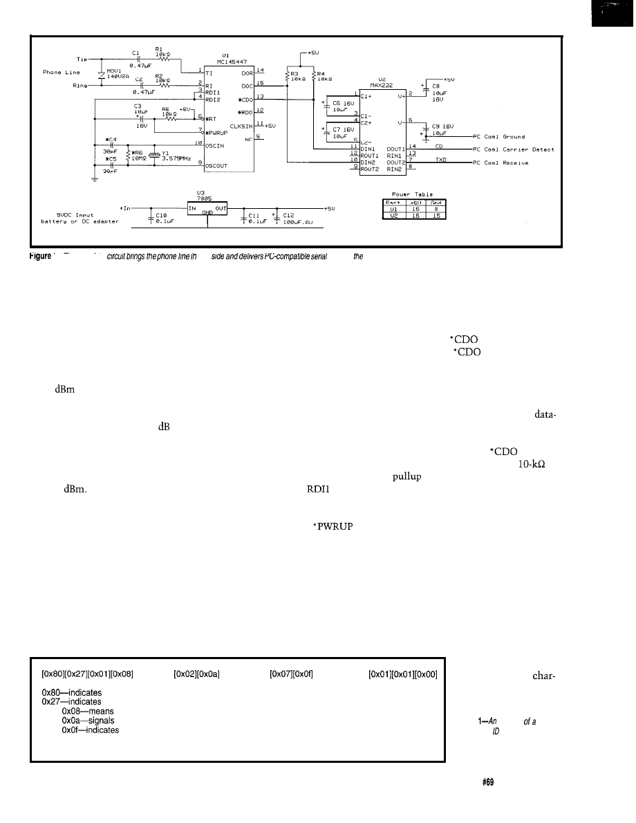
The Motorola MC145447 CID chip
has an analog front end, which inter-
faces to the telephone line with two
200-V nonpolarized capacitors
in series with two
resistors.
The input to the CID chip is differ-
ential. Because of this, it attempts to
decode any differential (AC) voltages
seen on the line, which results in occa-
sional periods of unintelligible garbage.
The data transmitted from the tele-
phone company is in standard Bell 202
format, similar to the format used by
the old
modems we all had a
few years ago [Bell 212). The data is
transmitted at 1200 bps with 8 data
bits, no parity checking, and 1 stop bit.
It is asynchronous, serial, and binary.
18
Issue
April 1996
Circuit Cellar
1-I
ne complete
one
data out
other
A logical 0 [called a space) is sent as
2200 Hz, and a logical
1
(called a mark)
is 1200 Hz. You can see there is noth-
ing special or proprietary about the
data. It comes to you exactly as your
PC would send it out its serial port.
If you’re using DSP to decode the
CID signal, the typical worst-case
amplitude of the transmitted signal is
-13.5
from the telephone com-
pany. The facilities (the wires traveling
though your town and ending at your
house) introduce another -20 of
attenuation.
This interference means that the
CID receiver demodulator should be
capable of decoding a worst-case signal
of -34.5
I chose the Motorola
device because it meets this worst-case
specification.
If you look at the schematic pre-
sented in Figure 1, you see that the
telephone line goes into one side of the
CID receiver chip and data comes out
the other side in inverted physical
format.
If you take this inverted data and
feed it into a MAX232 RS-232 driver/
receiver, it inverts the data and trans-
lates it into RS-232 standard voltages.
At this point, you’re ready to attach
the RS-232 data to a PC or embedded
controller and make a call to the chip.
When the CID data is decoded, it is
presented to the PC in an almost read-
able format. You can see the caller
name, telephone number, time, and
date along with some garbage data.
Since we aren’t making a stand-
alone box, but one that connects to a
PC, I disregarded any features for pow-
er saving or ring detection. You should
power the project from an isolated AC
adaptor.
RING SIGNALS
The CID receiver is forced to stay
active always because
and RD12
are held low and *RT is held high. A
standard delay-type reset circuit made
from C3 and R5 makes
go
low shortly after power is applied to
the circuit.
In this always-active mode, the data
out of the DOC pin attempts to decode
any signals on the telephone line,
including ringing voltages and occa-
sional DTMF signaling, during the
dialing of outgoing calls. This data
appears as garbage.
The circuit takes another signal out
of the CID chip on ‘CDO, which is
only high when valid CID data is being
received. The software of your system
ignores and flushes all characters re-
ceived when
is low.
As soon as
goes high, the
software buffers all received characters
in a queue. This technique ensures
that the queue always contains usable
data.
One discrepancy between the
book description of the device and my
real-world prototype is the drive capa-
bility of the DOC and
pins. I
found it necessary to apply a
resistor for the MAX232 to
receive the data correctly.
When you receive the Caller ID
message, it can be up to 80 characters
long and in one of two standardized
formats called fixed and variable. The
variable format is standard in North
America and is what I will discuss
here.
VARIABLE FORMAT
The variable-format service data is
one long data package divided into
subpackages. The first two characters
received in the data
package start with an
80 hex. The next
04301212
2145554141
Caller’s Name
the start of package indication
the total number of characters (hex) to be transmitted in the main package
0x01
that the date and time are coming next and are 8 characters
0x02
that the calling number is next and is 10 characters
0x07
that the calling name is next and is 16 characters
0x01 0x01-is the checksum
0x00-marks the end of transmission
Table
example
com-
plete caller stream from the
telephone company includes
name and number.
Circuit Cellar INK@
Issue
April 1996
19
is the number of characters total
to be transmitted.
The subpackages follow, starting
with a character that indicates the
type of subpackage (name, number,
date, time, service) and the total num-
ber of characters in the subpackage.
The subpackage types include:
l
0x0 l-date and time in DDDDTTTT
format
l
0x02-calling number
l
name
Table
1
offers an example of a package
and indicates what the separate com-
ponents of the package stand for.
If you decide to apply this circuit to
an application which doesn’t have
differential input, you should be able
to couple the signal directly into the
tip pin. Since you’re not using a differ-
ential input, this signal needs to be
twice the recommended amplitude to
activate the demodulator section of
the Motorola device.
Your software should sync on the
0x80 character and be able to accept
any package type next. There is no
guarantee that the subpackages will
arrive in a certain order nor that all
subpackages will be sent in a particu-
lar package.
If you find this hard to do in a single
supply system, you could add an in-
verting op-amp to the tip pin and apply
your signal to the input of the op-amp
and the ring pin. This modification
simulates a differential input to the
chip from an externally provided sin-
gle-ended input.
There are other subpackage types
EXPECTATIONS & APPLICATIONS
won’t elaborate on but which might
If you expected this article to be
indicate private or blocked calls. Typi-
deeply technical, you’re probably
cally, even if a subpackage meaning
thinking, “Gosh! This is really easy!”
private or blocked is sent, a number
package is also sent with an ASCII “P”
or “B” in the first character of the
called number field. Your software
should not always expect numeric data
for the number field.
Yes, it is. So, when you apply this
circuit or specification to your system,
if you use the Motorola chip as a caller
ID decoding block, it should be almost
plug-and-play.
All that’s left is the application.
You could have a window pop up a
caller’s name and number onscreen.
This read-out could be juxtaposed with
another window that holds notes
about the caller from a database and
include details such as account status.
Heh! Before you know it, you’re
enabled! You’ve found a perfect appli-
cation for Caller ID and you.
q
Richard Newman is an electrical engi-
neer living in Dallas, TX. He designs
specialized communications and in-
dustrial automation equipment either
in partnership or on contract. He may
be reached at
404
Very Useful
405 Moderately Useful
406 Not Useful
Visit our web site for a complete product
description and to get a working demo
or call
Software Development
3 PAR (32 BITS MAX)
32K RAM, EXP
-STANDARD PC BUS
-LCD, KBD PORT
BATT. BACK. RTC
IRQO-15 (8259 X2)
-8237 DMA 8253 TMR
-BUILT-IN LED
-CMOS NVRAM
USE TURBO C,
BASIC,
RUNS DOS AND
WINDOWS
EVAL KIT $295
UNIVERSAL
PROGRAMMER
-DOES 8 MEG EPROMS
-CMOS, EE, FLASH, NVRAM
EASIER TO USE THAN MOST
POWERFUL SCRIPT ABILITY
MICROCONT. ADAPTERS
PLCC, MINI-DIP ADAPTERS
-SUPER FAST ALGORITHMS
OTHER PRODUCTS:
8088
SINGLE
PC
BOARD COMPUTER . . . . . . . OEM $27 . . . l Q5
FLASH/ROM DISKS
16 BIT 16 CHAN ADC-D
. . . . . . . . . . . . . . . . . . 21 . . . . . 75
C CARD . . . . . . . . . . . . ...*.....
WATCHDOG (REBOOTS PC ON HANGUP) . . . . . 27 . . . . . 95
‘EVAL KITS INCLUDE MANUAL
BRACKET AND SOFTWARE.
MVS BOX 850
5 YR LIMITED WARRANTY
FREE SHIPPING
HRS: MON-FRI
EST
a
MERRIMACK, NH
.
(508) 792 9507
20
Issue
April 1996
Circuit
Cellar INK@
Willard Dickerson
Vehicular Control Multiplexing
with CAN and
Part
1:
Vehicular Multiplexing Fundamentals
plexing is a means
modules and/or subsystems through a
serial data link. The link is typically
one or two wires shared among several
modules [also called nodes).
Link sharing is facilitated by plac-
ing a special vehicle multiplexing
control unit at the interface of each
node. The main computer-controller
communicates with several distributed
nodes through the same port.
The nodes are automobile modules
such as sensors, ABS, audio system,
traction control, multi- or single-point
injection (gasoline engines), diesel
injection (diesel engines), cellular tele-
phone, cruise control, and so on.
This series overviews vehicular
control multiplexing and evaluates the
Motorola embedded controllers (the
in
and the
in CAN) in vehicular
multiplex devices. Part 1 describes
vehicle multiplexing as well as the
and CAN protocols.
In part 2, I’ll overview both the
and
I’ll
conclude with how these controllers
are implemented in their respective
and CAN networks.
VEHICLE MULTIPLEXING ORIGINS
The concept of vehicle multiplexing
comes from the computer-architecture
technique of local area networks. In
this concept, different nodes or mod-
ules share the same connection(s) for
data communication.
Each node in a distributed system
does not require a separate port into a
main computer. As a result, fewer
wires are needed to communicate
between units. This concept has been
used extensively in military aircraft,
heavy-duty trucks, and factories.
Since the increase in vehicle elec-
tronics resulted in excessive,
wiring harnesses measuring several
kilometers, automobile manufacturers
recently standardized reduced-wire
multiplexing in passenger vehicles.
DEFINING THE PROTOCOLS
or CAN can be described
from three vantages:
l
as a class of multiplex system
l
in its layers
l
as fields of information in its mes-
sage structure
There are three main classes of
vehicle-multiplexing systems: A, B,
and C. Class D is currently being de-
fined. The Society of Automotive Engi-
neers (SAE) characterizes classes by
transfer rates, recommended uses, and
intent.
Class A defines vehicle-multiplex-
ing protocols that support transfer
rates up to 10 kbps. This protocol is
typically used in trip or mileage com-
puters, electric windows,
driven switches, stepper-motor driven
devices, entertainment modules, and
so on. It primarily reduces cost, power,
CPU throughput, and
Class B protocols accommodate
transfer rates in the range of
kbps. They are typically used in engine
and transmission control functions
and cluster data passing. They are also
used for general-purpose applications
and legislated diagnostics (in accor-
dance with California regulations
expected to become law across the
U.S. by the year 2000).
Class C protocols support transfer
rates from 125 kbps to 1 Mbps. These
22
Issue
April 1996
Circuit Cellar INK@
rates are typically used in advanced
engine-control functions (e.g., variable
valve timing and fine-gear correction],
ABS, and suspension damping. Class C
is intended for systems requiring a
higher level of speed, intelligence, and
safety than Classes A and B.
If you look at vehicle multiplexing
protocols in terms of layers, each layer
describes a predefined set of physical,
electrical, or software characteristics.
For example, a physical layer de-
scribes the number and
MULTIPLEXING SCHEMES
Vehicle multiplex schemes typi-
cally provide more protection against
noise and signal corruption than older
serial protocols such as the
and
SPI. As a result, vehicle owners have
lighter weight cars with more reliable
communication links.
Typically, vehicle-multiplex
link controllers use fewer connections
and provide lower susceptibility to
automotive-related interference than
trollers, internal hardware and soft-
ware resources implement
multiplex protocols.
The partitioning of the multiplex
protocol is determined by available
hardware and software resources. The
partitions provide an overall project
structure. It determines whether the
multiplex controller is implemented in
an embedded controller or is stand-
alone, what application to load in the
CPU, what incremental loading is
length of lines needed to
communicate data at a cer-
tain speed. With the CAN
protocol, to transmit
1
Mbps,
you have a maximum line
*Optional for In-Frame Response
length of 100 m.
The type of transmission
Figure l--The
in-frame response is required for the
message-frame
for the 41.6 kbps PWM encoding.
buffers required for a proto-
col is also part of the physical layer. In
contrast, the size-of-message field is
described in another layer. Each proto-
col has unique requirements for mes-
sage-field sizes and arrangements.
Finally, the vehicle multiplex sys-
tem can be described in terms of its
message structure. This structure
defines the number and size of each
field, the type of information in the
fields, and how they are recognized in
a message.
For example, the message structure
of Class A and B protocols is not as
complex as Class C since Class C
protocols facilitate control over more
tasks in a shorter duration. Class A
protocols have lean message schemes.
Conversely, the complexity of
Classes B and C depends on their re-
spective applications. Class B tends to
communicate with a wider variety of
modules and is typically the most
complex message scheme.
Notably, the truck and bus vehicle
multiplex committee has taken the
(Class B) and put it on top of
CAN (Class C), thereby making a more
complex version of these protocols.
Class A and B direct functions like
automatic window motors, switches,
and simple LCD displays rather than
functions requiring substantially faster
bit rates and more diagnostic data.
However, Class C data link controllers
are capable of such simple applica-
tions, too.
the simpler, more traditional data
problem.
links.
A multiplexing scheme identifies
which node can communicate on the
shared link at a given time. There can
be seven nodes on a single link. Ve-
hicle multiplexing can take place via
frequency division, time division,
token slot, or token ring.
A scheme’s protocol specifies how
to implement the vehicle-multiplex
model. It provides a set of rules for
transmitter and receiver communica-
tion. Frequently, it includes error
checking, acknowledge methods, sig-
nal rate, and signal encoding.
necessary on the CPU from
each protocol layer, and
what the cost goals arc. In
many cases, partitioning
tradeoffs are made to meet
cost goals.
Additionally, simulation
can help determine the most
suitable partitioning for a
For instance, a verilog simu-
lation examines CPU use in a proto-
col-layer application. If the layer’s
throughput exceeds projected goals,
then alternate strategies are examined.
Error-checking schemes involve
parity checks, cyclic redundancy, noise
sampling, as well as simple or complex
error-handler routines.
The timing methods used in vehicle
multiplexing are either synchronous or
asynchronous. Data is transmitted
serially by one of a variety of methods,
which can include either communica-
tion mode.
Data flow for these methods can be
The protocol is implemented by a
simplex, half duplex, or full duplex.
protocol handler, which consists of
Whichever method is chosen, the
both hardware and software, depending
bit-rate clock is not transmitted
on the task’s complexity. Less
on a separate line but is embedded in
plex tasks are often done in software.
the data transmitted.
Sometimes, when vehicle-multiplex
Synchronous timing provides a
circuitry is found on embedded
known timing relationship between
applicalon
layer-where legislative diagnostics are found. Standard messages provide
information about the condition of systems affecting vehicle emissions.
presentation layer-consists of the addressing strategy, diagnostic codes, and their
parameters. The addressing strategy has both physical and functional modes.
Diagnostic codes and parameters are determined by legislative requirements.
session layer-places the system in an idle or sleep power-saving mode, or it can wake
up and alert the system when signals are present.
transport layer-includes message screening and filtering for hardware and software
and buffering for the bit, byte, or message level.
network layer-involves nondestructive arbitration in which the priority of a node is
determined by the message.
data link layer-involves bus communication, message format, synchronization, and
requirements for response to the message or message errors. See the text for
more information on the
message frame format.
physical layer-describes hardware performance aspects of the system such as bit rate,
bit encoding, drive type, redundancy, and media.
Table
l--The seven expanded
for the
can be embedded into three layers which are used in
Circuit Cellar INK@
Issue
April 1996
23
let you adapt your
to
Now,
Field Programmable Gate Arrays
can double your
by
you
change your product’
on-the-fly.
But how do you quickly learn the
of
microcontrollers?
The
epX31
IS
your
It has
you need to
and test
the
used
thousands of embedded designs,
a RAM-based FPGA with
3,500 reconfigurable
gates,
for
The FPGA amplifies
capabilities of
the 803 Program the EPX780 to create
custom address decoders, new Interrupt
sources,
timers, specialized
real-time bus monitors and
more! The only
IS
your ingenuity!
It’ s easy to use the
You get a
complete
on FPGA design with
our
text. Or modify one
of our design examples for your own
u s i n g t h e
and
i
included
the epX3 Next, load the
FPGA
+ 8031
code
the epX3 through the PC parallel
port. Then apply real-world test signals to
your
under the control of your PC.
The
grows with your
You can cascade several epX3 to build
multiprocessor or multi-FPGA
systems.
Or connect special-purpose chips to the
epX3 through the breadboard interface
The
epX31
lets you try out more
less effort
No more un-
tangling wire-wrap or patching prrnted
circuit boards. Just reprogram the static
RAM and you’ re ready to try again
That
a
back on vour face from
So will
board
cable
assembler
modules
Workout text
(800) 549-9377
INTL:
(919) 387-0076
Check our Web site for FPGA
tutorials!
RTR Bit
CRC
Reserve Field
ACK Bit
Data Length Code
ACK Delimiter
Bus
Idle
,
, D a t a F i e l d
CRC Field
0 to Bytes
, , , End of Frame Interframe Space
7
3
Arbitration
Acknowledge
of Frame Field
Field
Figure
CAN message
frame format includes a parity bit in the CRC field.
transitions. The width of a bit repre-
the bits and bytes. The bytes are trans-
mitted continuously until a condition
halts or suspends their transmission.
The receiver recovers the clocking
from transitions in the data. This tech-
nique allows fewer lines to be used
than standard SPI controllers, which
usually provide a separate line for the
receiver clock.
senting one or zero is the same, which
allows infinite bits per transition. No
edges are present if the same bit is
asserted continuously.
Conversely, asynchronous control-
lers have a variable relationship be-
tween bits and bytes. That is, each bit
can be transmitted separately or in
groups. Typically, a start bit synchro-
nizes the transmission.
The NRZ scheme offers a low num-
ber of transitions per bit (hence low
emissions) and fixed transition or sam-
ple points.The bipolar version requires
twice the voltage swing as the unipolar
scheme.
ENCODING
Vehicle-multiplex messages are
usually encoded to:
On the other hand, NRZ accumu-
lates clock errors among nodes, mak-
ing it harder to synchronize the bits.
This characteristic is a major nuisance
in vehicle multiplexing since the clock
is not transmitted on a line separate
from the information. This problem
can be solved by bit stuffing.
l
reduce emissions in a harsh
the-hood environment
l
improve recognition of bits during
arbitration for single-wire systems
l
reduce physical media costs by facili-
tating single- or dual-wire systems
Bit stuffing guarantees at least a
bit transition every bits. A bit of the
opposite polarity is inserted each time
five consecutive or are detected.
The receiver understands and uses the
same rules by deleting the inserted bits
from the stream.
The common encoding types in-
clude
to Zero (NRZ), Pulse
Width Modulation (PWM), Variable
Pulse Width Modulation (VPWM),
Frequency Modulation (FM), Modified
Frequency Modulation (MFM), and
Manchester.
The method of encoding is deter-
mined by cost, bandwidth efficiency,
and the EM1 imposed on a given sys-
tem. Cost increases with the more
complex devices and circuits of certain
schemes. Bandwidth efficiency be-
comes critical for higher-speed multi-
plex protocols such as CAN. The EM1
is essentially affected by the number of
transitions per unit time a waveform
generates and data encoding.
PWM encoding represents each bit
by varying the pulse width of periodic
signals from one-third to two-thirds.
The shape of the pulse and approxi-
mate locations of the edges are fixed
during each periodic signal. It can use
two edges on the data link for each bit
transmitted. This encoding is com-
monly found in
equipment with
data rates of about 10.4 kbps.
PWM offers defined sample points,
fixed bit lengths, the ability to arbi-
trate wired or contention buses, and
the ability to
all receiv-
ers on a rising edge of each bit.
NRZ encoding represents data with
unipolar (above ground) or bipolar
Conversely, PWM is less cost effec-
tive than an automotive data link (i.e.,
single wire). The dual edges increase
radiated emissions. It’s therefore more
difficult recognizing bits, especially
with extreme ground offset.
24
Issue April 1996
Circuit Cellar INK@

VPWM represents a binary signal by
varying a pulse within periodic bound-
aries. Unlike PWM, however, the vari-
ations in the pulse and edges can alter
within each periodic pulse.
FM is represented by periodic clock
pulses signifying a one if intervening
time slots are pulsed or a zero if no
change occurs. This technique ad-
versely effects radiated emissions since
several edges can potentially be gener-
ated at higher frequencies.
MFM encoding is similar to the FM,
except that it eliminates the clock
pulses unless the data remains con-
stant for more than two consecutive
bits. The pulses can be replaced with
transitions. That is, a one is signified
by a transition, and a zero by no transi-
tion. Unfortunately, there is more
complexity distinguishing between
clock pulses and logical transitions.
This problem can be resolved due to
the
bit times for
Additionally, arbitration is more
complex with MFM than FM because
for any given bit position, either a one
or a zero has higher priority depending
on the previous bit stream.
Manchester encoding is represented
with transitions. It defines various
fixed bit times (e.g., 96 for 10.4
kbps) and forces a transition at each
defined boundary. A one is signified by
an additional transition triggered in
the middle of a bit time, and a zero by
an unchanged pulse during a bit time.
51850 OVERVIEW
one-wire system and the higher
is a one- or two-wire serial
protocol for low- to medium-speed
mission speed (41.6 kbps using PWM)
vehicle-multiplex applications. The
lower transmission speed (IO.4 kbps
in a two-wire system
falls under
using VPWM) is implemented in a
the Class B protocol, and emissions are
in-between those of NRZ and PWM.
This protocol-or variations of
is used by domestic automotive com-
panies. It controls such devices as
window motors and lock solenoids,
digital instrument display,
brakes, and fault communication
As with other vehicle multiplex
schemes, this protocol consists of a
synchronous multimaster bus system.
Multiple units connect to the same
bus, and any unit can request control
of the bus. Through arbitration, one
unit is selected to master the bus.
This protocol offers:
l
open architecture
l
moderate complexity
l
single-level bus topology
l
multimaster peer-to-peer
l
legislated diagnostics
As an open architecture,
al-
lows prioritization of frames and is
compatible with CSMA/CR.
Moderate complexity reduces cost
because it requires less hardware and
software, which in turn decreases
development and maintenance costs.
A single-level bus topology provides
one link so all nodes transmit and
receive from a single path. It receives
all frames simultaneously.
A multimaster system enables mul-
tiple nodes to request access of a bus
(i.e., any node can potentially be the
master). This approach also reduces
hardware and development costs since
no special hardware and software is
required for a separate or additional
master node.
1997.
Layers provide a standard means to
categorize and describe fundamental
hardware and software architectural
characteristics of a vehicle-multiplex
Legislated diagnostics consist of
automated tests for vehicle emissions
or any other environmental test re-
quired by law. These tests go federal in
physical layer-consists of its drive capability, bit level, and format and transmission
medium.
transfer layer-includes message framing and arbitration, error detection and report,
and fault confinement.
object layer-includes message buffering, acceptance filtering, and prioritized message
handling.
application layer-presents the hardware and software trade-offs which are dictated by
the specific application.
Running under
Windows?
a standard
acquisition
b o a r d
old
but
there is a
better way.
S t a n d a r d d a t a a c q u i s i t i o n
b o a r d s c a n u n k n o w i n g l y
sabotage your data. Ensure
the integrity of your results.
Windows Optimized
5800 Series gives you the
resources you need:
Channel Gain RAM, Dual
DMA, aggressive prices,
and
some of the best noise
performance in the industry!
5801MF:
16
A/D,
2
D/A, 40 digital
5803HR:
16 channel
A/D,
2
D/A, 40 digital
learn more
voice
800-648-6589
fax
617-938-6553
web
http://www.adac.com
info@adac.com
Table
CAN layer information includes four basic layers.
American Data Acquisition Corporation
70 Tower Office Park, Woburn, MA 01801 USA
Circuit Cellar
Issue
April 1996
Table
and CAN
are similar in some
and quite different in others.
format is required for the
PWM and not
for the
VPWM
As you can see in Figure 1, the
frame response format consists of a
start-of-frame signal (SOF); header,
data, and error-check field; end of data
more data; and
frame (EOF) check field
Notably,
the error field is optional with the
frame response format for
VPWM
is
sent to (i.e., under the hood,
vehicle, rear trunk, etc.)
engine or traction control). It handles
the number of messages required at a
The final section of data pertains to
three bytes of control and status infor-
mation. The control information is
acted on by the parameter owner, and
the status is used by the
monitoring or controlling nodes.
latency sufficient for the algorithms of
these applications.
The common arbitration method
used for the
bus is nondestruc-
tive. The message with the highest
priority is transmitted, while transmit-
ters losing arbitration simply cease
transmitting until they receive an idle
bus transmission.
At times, however, automotive
manufacturers use a simplified subset
of CAN for less stringent applications
like controlling window or seat adjust-
ment motors, or door-lock solenoids.
system. Table 1 illus-
trates the seven layers of
the typical
system
can include.
In practice, however,
these seven layers reduce
to three. The presenta-
tion layer embeds in the
application layer, just as
the session, transport,
and network layers are a
part of the data link
layer. Only the physical
layer stands alone.
The message-frame
Features
C A N
Common bus waveforms
VPW, PWM
NRZ
Number of basic frame formats
Number of bus wires
(VPWM) 2 (PWM)
4
Maximum frame length
2 wire, twisted pair
101 bits or 12 bytes
bits
Bus rate
10.4-41.67 kbps
Arbitration method
126 kbps-1 Mbps
Error checking (8 bits basic)
priority ID encoding
priority ID encoding
CRC (15 bits)
Low-power modes
CRC (15 bits plus parity)
suspends clock and
suspends clock and
(implementation dependent)
tristates the bus
tristates the bus
Number of descriptive layers
3 (7 expanded)
4
Methods to initiate transmissions
bus wakes device from low-power mode,
bus wakes device from low-power mode,
receive or send request for transfer,
receive or send request for transfer,
or external control asserts control signal,
e.g., a CPU writes to a control register
or external control asserts control signal,
Limits on bus length
40 m (35 t 5 for tester)
e.g., a CPU writes to a control register
130 m for 50 kbps
at 41.6 kbps
Method of selecting receivers on bus
or 20 m for 1 Mbps
message broadcast
message are broadcast
and arbitrated across bus
and arbitrated across bus
Maximum number of nodes on bus
32 at 41.6 kbps
100 at 50 kbps
A standard
system requires
the examination of four types of errors:
cyclic redundancy check (CRC), frame
length, out of range, and invalid bit,
byte, and symbol detection
The first two errors are typically
decoded by examining the number of
bits or bytes within partitions of a
transmission. However, the latter two
error types are detected through a form
of digital or analog filter.
The maximum number of nodes on
the
bus depends on bus speed,
wire length, and drive strength. For
example, 32 nodes can be driven on a
40-m bus.
CAN is commonly found in Euro-
pean vehicles. Typically, it is more
expensive to implement than
because of its complexity. It can be
used for applications such as low-level
laptop computer communication,
engine control, ABS communication,
and the applications common to
The CAN protocol provides
tolerant requirements at transmission
rates of 125
Mbps.
The message structure of the
protocol is partitioned into header and
data bytes. Standard
allows a
maximum of 101 bit times or 112
bytes per message, excluding the SOF,
EOD, NB, and EOF fields. The header
consists of three bytes which include
an introduction to the type of message,
the functional or physical address of
the receiver, and the physical address
of the sender.
The final partition consists of three
CAN OVERVIEW
The CAN protocol originated over
14 years ago in Germany by Bosch
This fairly complex,
speed protocol offered a solution to
reduce the size of wiring harnesses and
power for distributed loads while im-
proving the noise susceptibility be-
tween these nodes.
The CAN protocol can also be de-
scribed in terms of layers
Table 2
defines its four basic layers: physical,
transfer, object, and application.
CAN messages are communicated
through four frame types: data, remote,
error, and overload.
sections of data information. The first
two sections present O-8 bytes while
the last two sections consist of three
bytes. The first two sections of data
provide information about the type of
message ID, the message ID number,
and control signals that point to the
proximity or vehicle section a message
The CAN protocol can be described
by the same characteristics as the
speed-performance, advantages,
layer information, message format, and
so on. The CAN protocol is considered
suitable for, but not restricted to, a
Class C controller.
The data frame communicates data
between nodes. It consists of a start bit
or signal, 1 l-bit message identifier,
remote transmit request (RTR) bit,
reserved bit, 4 bits for data-length code
(DLC), data field consisting of O-8
bytes,
CRC field, two acknowl-
edge bits, and an end-of-frame field.
Figure 2 depicts a data frame.
Automotive manufacturers use this
complex protocol because it’s suitable
for relatively complex operations (e.g.,
The message identifier represents
an address that can be a physical, func-
tional, or combination. The DLC rep-
resents the length of the data field.
26
Issue
April 1996
Circuit Cellar
The acknowledge bits inform the
transmitter that at least one node
received the data correctly.
The remote frame is the same as
the data frame, except that it does not
include the data field. The frame is
used by the receiver to request data
from the transmitter. This data is sent
in the subsequent data frame. The
message ID of this data frame matches
the requesting remote frame’s ID.
The RTR bit determines whether a
frame is data or remote. Data is indi-
cated by the dominant RTR bit, and
remote by a passive RTR bit.
The error frame indicates an error if
an undesired condition is detected by a
node. The detected errors from data or
remote frames are transmitted after
the respective frame.
Finally, the overload frame invokes
additional delay between adjacent data
frames and remote frames.
The common arbitration methods
used for the CAN protocol establish a
polling or priority scheme between the
various ID fields found within the data
or remote frames.
The number of the units or nodes
found on a CAN bus are determined by
the drive strength of the CAN nodes
since each can be a master and by the
wire length that attributes to loading.
Typically, CAN is on two-wire bus
connections. Sometimes, a one-wire
scheme is used for limited applica-
tions. The two wires are twisted pair
without a separate transmitted clock
or with one wire transmitting the data
and the other a synchronous clock.
AND CAN PROTOCOLS
The major aspects of the
and
CAN protocols are in Table 3.
Next month, I’ll overview the pro-
cessors embedded in
and CAN
to see just how they’re implemented in
their multiplexing schemes.
q
Willard Dickerson is a design project
leader for
RISC-embedded con-
trollers in Motorola’s Advanced Mi-
crocontroller Division. He develops
hardware and firmware for and
bit embedded controllers. He may be
reached at
“SAE Recommended Practice
Class B Data Communica-
tion Network Interface,” 1993.
M. Nagao, et. al., “Bus Driver IC
for Use in Vehicle Multiplexing
Communications,” Proceedings
of 5th Annual IEEE, 79-82, 1992.
Mark P.
and A.J.
meyer, “Message Structure and
Strategy to Drive SAE
Networks: An Introduction to
SAE International
Congress and Exposition. De-
troit, MI. Feb. 24-28, 1992.
Motorola,
Central Pro-
cessing Reference Manual,
Man-
ual
1993.
Sarjay Gupta, “CAN Facilities
In-Vehicle,” Society of Automo-
tive Engineers, 1990.
407 Very Useful
408 Moderately Useful
409 Not Useful
Advanced Vehicle Technologies
multiplex bus products support
the design and testing of vehicle
network components.
n
Automotive
Bus
VPW, PWM,
. Analog Digital Hardware
Design
. Embedded Software/Firmware
Development
. PC Based Software Development
. Hardware Software Systems
Engineering
custom Prototype Software
Hardware Development,
Assembly, and Test
We can provide you
expertise, products, and
Contact us
Advanced Vehicle Technologies, Inc.
Circuit Cellar INK@
Issue
April 1996
27
Anindya Ray Lee Hanson
The Embedded Sun
Part 1:
Introduction to the Hardware
here’s an adage
that says if you’ve
got a good thing go-
ing, don’t change it-or
if you do, change it minimally.
Over the years, Sun Microsystems
SPARC Technology Business has been
successful with its high-performance
SPARC microprocessor architecture. It
recently announced its newest chip,
the
64-bit microproces-
sor, which includes an integrated mul-
timedia instruction set.
Therefore, it only makes good engi-
neering and business sense to parlay
Sun
previous processor archi-
tecture, technology strengths, and
development efforts to help design and
develop the new
This
chip (see Table 1 for complete specifi-
cations) targets three high-end embed-
ded-system applications: networking,
telecommunications, and printer/
copier.
The
will be an-
nounced in April ‘96 with
quantity shipments scheduled for the
third quarter of 1996. The chip is a
derivative of the
Sun’s
low-end workstation processor (re-
leased March 1995).
has an integer unit
(IU) with an eight-window SPARC
register file, high-performance
point unit (FPU),
instruction
cache,
data cache, 64-entry mem-
ory-management unit (MMU), DRAM
interface, and
controller.
This article explains how these and
newer functional blocks and features
are used in the design of the micro-
SPARCIIe. In designing this micropro-
cessor, our engineers focused on four
main design goals. They wanted to
develop:
l
a microprocessor that is cost-effec-
tive for high-end embedded-systems
markets, which could be reduced in
cost over time to meet evolving
embedded-system requirements
l
a flash memory interface that en-
ables customers to run real-time
operating systems (RTOS) and load
and run their own code out of ROM
(see
“Streamlining User
Development”)
l
bus-interface capability for cus-
tomers currently using Sun prod-
ucts. This feature provides a way to
move from SPARC legacy code and
capability to
at their own
pace.
l
a high-performance direct-memory
interface that permits data to move
back and forth quickly
The key to a large part of micro-
performance is its ability
to implement a system with few exter-
nal interface components. In this case,
you don’t need external memory con-
troller, I/O device controller, and ROM
controller chips. The chip’s perfor-
mance is 85 SPECint92 and 70
fp92
Dhrystones with
CPU clock, a
clock, and
clock.
ARCHITECTURE
As Figure la illustrates, the micro-
SPARCIIe microprocessor contains
eight basic sections: IU, FPU,
I-cache, 8-KB D-cache, 64-entry MMU,
memory interface, flash memory inter-
face, and
interface. The processor
also includes an interface to the
bus via a bridge chip since the
interface pins are not currently de-
signed for direct PCI-bus communica-
tion.
The bridge chip, known as Falcon,
is composed of a
device controller,
28
Issue
April 1996
Circuit Cellar INK@
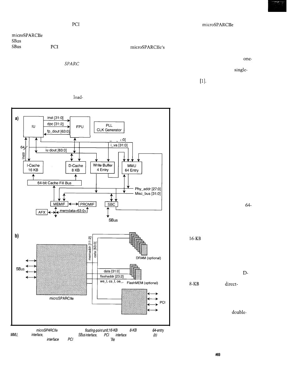
DMA transfer controller, and configu-
ration registers that define the
addressing space (see Figure I b). The
supports up to four
slots via its direct interface to the
and up to four
slots through
the bridge chip.
The IU executes the SPARC integer
instructions defined in the
Architecture Manual V. 8. It contains
136 registers comprising 8 windows of
16 register sets and 8 global registers.
The IU operates on prefetched instruc-
tions, using a five-stage pipeline.
Branch folding and single-cycle
is correctly predicted.
and-store instructions improve its
throughput.
Branch folding is a technique used
for reducing the delay of branch pro-
cessing. Branch instructions are de-
tected early in the
pipeline, and the instruction flow
follows the predicted outcome of the
branch.
Since branches are removed from
the instruction stream before they
execute, the integer unit can handle
two instructions at once if one is a
branch and the outcome of the branch
d va 131
memadr bus
32-bit
Falcon (optional)
Figure l-(a) The
has an integer unit,
f-cache,
D-cache,
A four-deep store buffer can hold
memory
flash memory
interface,
and bus
via a bridge chip. The
data stored from the IU or FPU to
bridge chip’s function is to
to the
bus on one side and to the on the other.
memory or other physical devices. The
By predicting that all branches will
be taken, the
uses
simple prediction algorithms. If the
prediction is correct, branch folding
occurs, and no bubble exists in the
execution pipeline. If the branch is not
taken, execution continues with the
next sequential instruction after a
cycle delay.
The FPU fully executes all
and double-precision floating-point
instructions Quad-precision in-
structions trap in software and are
implemented there. The FPU contains
32 x 32 f registers, a general-purpose
execution unit, and an FP multiplier.
In most instances, these architec-
tural features enable the parallel ex-
ecution of an F P MU L and another FP
instruction. A three-deep queue of FP
instructions is provided to increase the
efficiency of concurrent floating-point
and integer execution.
The MMU translates the 32-bit
virtual addresses of each running pro-
cess to 3
1
-bit physical addresses. The
three high-order bits of the physical
address are maintained to support
memory mapping into eight different
address spaces.
The MMU also serves as an I/O
MMU and controls arbitration be-
tween I/O, D-cache, I-cache, and TLB
references to memory. It contains a
entry fully associative TLB, supports
256 contexts, and protects memory so
that a process is prohibited from read-
ing and writing the address space of
another process.
The
I-cache is direct mapped,
virtually indexed, and virtually tagged.
It’s organized as 5 12 lines of 32 bytes
plus 32 tag bits. Cache refill is per-
formed four 64-bit words at a time.
Cache streaming and bypass are each
supported for both the I-cache and
cache.
The
D-cache is a
mapped, virtually indexed, virtually
tagged write-through cache with no
write allocate. Data store is organized
as 512 lines of 16 bytes, plus 32 tag
bits. Single-word integer and
word FP read- and write-cache hits
take only one clock cycle.
Circuit Cellar INK@
Issue
April 1996
29
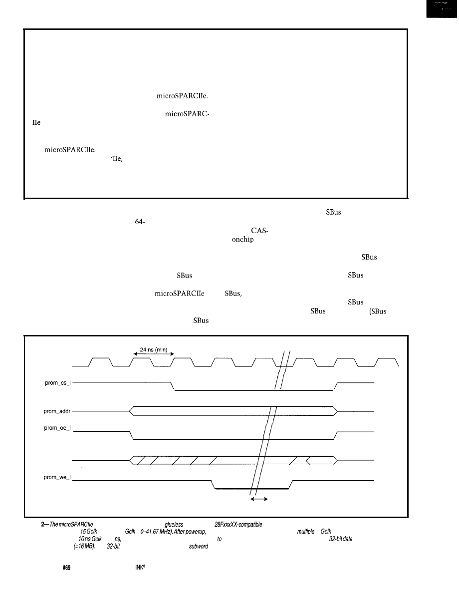
Streamlining User Development
As a major part of our second goal, we analyzed the
needs of embedded-products users. We found that cur-
rently used printer, telecom, and networking systems are
based on general-purpose high-end microprocessors. We
therefore looked for ways to provide embedded-systems
engineers a clear advantage when using
Here’s one distinct advantage. A considerable amount
of code is now readily available to support
as well as other existing SPARC processors. More
than 50% of all embedded-applications software is devel-
oped on Sun workstations and can be directly ported to
the
By porting code to the
both software and hard-
ware engineers save a great deal of time-time otherwise
needed for emulation and cross-compilation. Debugging
code via in-circuit emulation can consume weeks of
engineering resources. As a conservative estimate, it
often takes as much as 20% of the overall development
cycle.
A number of third-party development tool companies
support this concept of development and deployment on
the same platform. Such vendors as Wind River, Force,
Lynx, Sun, and Microtech offer both operating systems
and debuggers which run on Sun desktop machines and
port directly to the embedded application.
It’s prudent to maintain engineering familiarity with
the same tools and avoid cross-compiling. By developing
and deploying on the same architecture, you avoid the
problems associated with the classic routine of develop-
ing on a platform, cross-compiling from the target micro-
processor, setting up the emulator, and debugging.
store buffers are 64-bit registers. As in
the I-cache, cache refill is done two
bit words at a time.
The DRAM memory-interface con-
troller generates all the signals neces-
sary to support up to 256 MB of system
memory. The DRAM bus is 64 bits
wide with two parity bits, each one
covering 32 bits of data. System
DRAM is organized as eight banks,
each of which may be 2, 8, or 32 MB,
depending on the size of the DRAM
used.
RAM-refresh-control logic provides
complete DRAM refresh control, and
the refresh controller performs
before-RAS refresh. The
re-
fresh control is programmable, and
self-refreshed DRAM
S
are also sup-
ported.
The
interface performs all
functions necessary to connect the
to the
including
dynamic bus sizing, cycle rerun con-
trol, burst-cycle reordering, arbitration,
and general
control. This inter-
face controls
devices sharing the
bus and supports the following trans-
actions:
l
Programmed Input/Output (PIO)
between the CPU and
devices
l
Direct Virtual Memory Access
(DVMA) between
masters and
local resources (Local DVMA)
l
Direct Virtual Memory Access
(DVMA) between
masters and
other
slave devices
DVMA)
Gclk
(for read cycle)
prom-data
(for write cycle)
Programmable Latency
Figure
flash-memory interface provides
connection to
flash-memory devices. The read/write cycle shows programmable
latency, which defaults to
if desired (1
=
this latency can be reprogrammed to any
of
between 2 and 15. For example, if
the ‘//e’s internal clock is
is 30 and if f/ash-memory latency is programmed 4, it becomes 120 ns. This latency is based on a
bus, with an address
range of 4 megawords
Only
word accesses are a//owed, so
accesses require a read-modify-write sequence.
30
Issue
April 1996
Circuit Cellar
DSP
in
Embedded Processors
by Richard Pedreau
new
family
of 32-bit SPARC-compatible micro-
controllers comes with integrated
DSP functions.
To optimize the
functionality tradeoff,
approach is to find out which DSP
functions are necessary in the dedi-
cated field targeted by each of the family’s products. It then integrates
those functions as hardware
during product definition.
This methodology offers two advantages:
l
DSP functions are deeply integrated in the CPU and use the regular regis-
ter file and instruction set. They are considered part of the CPU core
rather than an add-on.
l
it follows SPARClet’s basic rule-maintain the development chain con-
sistently and avoid a cross-development or dual-processor environment.
CPU and DSP cores usually have to be programmed separately, which
generates extra code-writing and debugging.
The TSC701, the first member of the SPARClet product line launched
by TEMIC in 1996, is a good illustration of this strategy. Its dedicated tar-
get is the low-end communication market [hubs, routers, ISDN adapters,
cellular base stations, etc.).
Most emerging applications use an additional DSP core to implement
filtering algorithms based mainly on iterative multiplication. The TSC701
addresses this issue by including a 32
x
or
fully parallel
Multiply-and-Accumulate (MAC) unit.
In contrast, the highest-performing DSP cores perform one-cycle multi-
plication. Despite this, the TSC701 achieves the same or even higher over-
all performance for a lower cost.
What are the challenges?
l
The
have x- and y-buffer input queues (previously stored by the
main processor) that must be loaded from external memory. The
701’s MAC unit uses regular window registers as operands and result. So,
bus traffic is reduced by two.
l
The TSC701 multiplier takes four or five cycles, depending on whether
the accumulation register is the same as before. But, during this time,
the Load/Store Unit can load the next two operands.
Thus, the TSC701 remains very close to the one-CPI (Cycle Per Instruction)
rate on the whole loop. Such a rate is unreachable by most
associations (which use dual-port RAM most of the time) because of the loss
in main-processor-to-memory and memory-to-DSP buffer transactions.
Use of a secondary DSP remains valid in configurations employing all
the DSP functions. However, in embedded applications requiring intensive
use of just a few DSP functions, it makes much more sense to integrate
them into the main controller.
For other products being introduced in the same product line, TEMIC
follows the same approach: it fits the DSP capabilities of each derivative to
its targeted application field.
(
C
O
N N
E C
TS
Rs-232)
AR-16 RELAY INTERFACE (16 channel) . . . . . . . . . . . . $ 89.99
Two 8 channel (TTL level) outputs are provided for
AR-2 RELAY INTERFACE (2 relays, 10
44.99
RP9 REED RELAY CARD (8 relays, 10
RELAY CARD
amp SPDT, 277
A N A L O G
D I G I T A L
To Rs-232)
CONVERTER* (16
AD CONVERTER* (9
Input voltage, amperage. pressure.
light,
joysticks and a wide variety of other types of analog
signals.
available (lengths to
Call
for info on other A/D configurations and 12 bit
converters (terminal block and cable sold separately).
Includes Data Acquisition software for Windows 95 or 3.1
TEMPERATURE INTERFACE* (8
Includes term. block 8 tamp. sensors
to
STA-9 DIGITAL INTERFACE* (8
Input on/off status of relays, switches, HVAC equipment,
security devices, keypads, and other devices.
SELECTOR (4 channels
an
port into 4 selectable
CO422 (RS-232 to RS-422 converter) . . . . . . . . . . . . . . . . . . . 39.98
l
EXPANDABLE...expand your interface to control and
up to 512 relays, up to 576 digital inputs. up to
128
inputs or up to 128 temperature inputs using
expansion cards.
l
TECHNICAL
over the
by our staff. Technical
disk
test software&pro
i n
GW Basic,
Turbo C, Assembly and others are provided.
for
24
hour
industrial
10 years of
in energy management
Circuit Cellar
Issue
April 1996
33
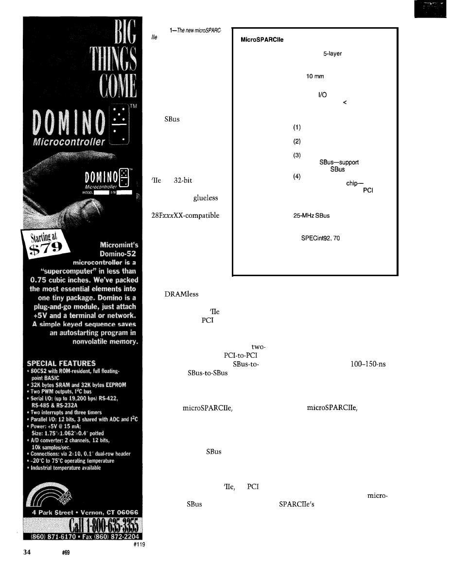
Table
targets three high-end
embedded-system applications:
networking, telecommunications,
and printer/copier.
The
interface
works with the MMU
to arbitrate the system
and memory resources
and for I/O address
translations.
System Level
Architecture:
Integrated on the
is a
flash-
memory interface
which allows
connection to Intel
flash-memory devices.
This interface has a
software-program-
mable latency (de-
scribed later). It’s
suitable for embedded
systems which take
advantage of diskless
and
small form-factor sys-
tems.
Direct programmable
DRAM interface
Direct interface to
flash memory
Direct interface to
for up
to 4
slots
Interface to PCI bus
via bridge
supports up to 4
slots
Clock Speeds:
33-MHz 32-bit PCI bus
CPU Speed:
125 MHz
Performance:
85
SPECfp92,
160 Dhrystones
On-Chip Memory:
16-KB instruction cache
8-KB data cache
Also new to the
is direct hook-
up to the Falcon
bridge chip. This
feature gives a transition path to ac-
commodate the growing industry ac-
ceptance of PCI. Falcon provides
way XI-to-DRAM and
DMA capability similar to
DRAM and
DVMA.
To save device pins, the flash mem-
ory interface block shares the data bus
with the DRAM interface and has
extraneous control for writing to flash
memory. Supported flash memory
devices include Intel parts in the 28F
series.
These devices have specified access
times of approximately
access period, and data widths are
typically 8 or 16 bits. These flash
memory accesses are about one-third
to one-half as fast as DRAM ones.
In the
the flash
access is kept to 32 bits at all times.
From a software perspective, the flash-
memory access behaves the same as
the DRAM access, even though it is
physically addressed in a different
address space.
Specifications
Process:
Transistors:
Die Size:
Power:
0.5 micron,
metal CMOS
One million
10x
Fully static, 3.3-V core
5.013.3-v
Power-down mode 10% of nominal
Peak power 7 W
MODULARITY
As one of our major strategies in
designing
we wanted
to make the functional blocks as mod-
ular as possible.
For example, modular design en-
ables future elimination of the FPU if
desired. Also, the
interface can be
omitted to comply with certain other
embedded-systems design require-
ments.
In derivatives of the
the
interface can be brought on-chip, re-
placing the
interface. Cache sizes
can also be modified or, in applications
where data caching is unnecessary,
eliminated entirely.
All flash-memory accesses can be
cached similarly to DRAM accesses.
Thus, you can run tight-looped code
from within cache. Also, the
flash-memory interface
has programmable latency. This fea-
ture can be important to the embed-
ded-system designer who wants to
Issue
April 1996
Circuit Cellar INK@
Fujitsu’s SPARClite Alternatives
by John Bums
Fujitsu’s latest entries in the embedded market, the
and
MB86936, have met with success in imaging and communications ap-
plications.
The newest parts carry on the tradition Fujitsu began in 1990, when
they adapted the SPARC architecture specifically for embedded applica-
tions where price and performance are paramount.
Both new processors include the popular features of previous family
members and maintain code compatibility. Both integrate peripherals
to minimize glue logic.
The
is intended for applications which require excellent
performance at the lowest possible cost. The MB86936, with on-chip
FPU, three DMA channels, and a video-rasterization interface for prin-
ter applications, is geared for high-performance applications.
To achieve superior performance, the
is built around the
SPARClite integer core. The core features a five-stage pipeline which
operates at a sustained rate of 1.08 CPI.
Additions to the SPARC architecture, pioneered by Fujitsu to en-
hance embedded performance, include hardware MU LT I P LY, I V I DE
STEP, and SCAN instructions.
To show the benefit of the SPARClite SCAN instruction, consider a
code segment that compresses long binary strings by looking for runs of
all ones or zeros and coding these so
reconstruction is possible.
Each instruction runs one cycle out of the instruction cache if it is in
the active path for a particular case.
Without a hardware implementation of SCAN, which takes one cycle,
an additional software routine requiring 43-52 cycles would be needed.
This routine would also consume instruction-cache space. Designers of
communications applications find SCAN useful where there is a large
amount of I/O management.
The D I V I DE STEP instruction was also implemented for embedded
applications without deterministic interrupts. D I V I DE STEP executes a
32 x 32-bit division in less than 40 clock cycles and efficiently handles
an interrupt at any point without losing the division in progress. The
multiplier provides 64-bit results in only
clock cycles.
The
is manufactured in
CMOS process and
runs at 25 MHz. It features a l-KB direct-mapped instruction cache.
Evaluation of standard and customer benchmarks shows that instruc-
tion cache contributes more than data cache to performance. As with
previous members of the family, cache lines can be individually locked.
To facilitate low-cost system design, the
features:
l
a configurable data bus which supports
or
memory
l
a bus interface which provides programmable chip selects and pro-
grammable wait-state circuitry
l
an on-chip interrupt controller which handles up to 15 interrupts with
external priority encoder or 4 external
interrupt requests
l
a complete DRAM controller which supports
5
1
-MB,
and 2-MB configurations in up to two banks
l
a fully static circuit design which enables the processor clock to be
slowed or stopped to conserve power with no loss of internal state. In
normal operation, power consumption is l-l W
Circuit Cellar INK@
Issue
April 1996
35
As a result of these features and a price of less than
precision operations except DIVIDE and SQUARE ROOT
$15 in high volume, the ‘933H has been designed into a
are executed in one clock cycle, as are double-precision
new generation of digital cameras that provide
ADD and SUBTRACT. This capability has proven
ment-ready images and bar-code readers that use
tive for both color laser printers and machine-vision
dimensional bar codes,
applications.
The MB86936 is designed for high-performance
All SPARClite processors comply with both V. 8 and
cations and offers many more features integrated
V. 8E (the embedded extension of V. 8) of the
chip. The part is manufactured in OS-micron CMOS,
Architecture Manual
and execute all the SPARC integer
and its SPARClite core runs at up to 50 MHz in
instructions it defines. Typically, SPARClite processors
doubled mode. Less-expensive memory systems can be
feature a register window scheme consisting of 136
used with the bus running at 25 MHz.
registers configured in eight windows of 16 register sets
To minimize system cost and reduce glue logic, the
and 8 global registers. The
reduces the
MB86936 has an integrated DRAM controller, providing
ber of windows to six.
an address multiplexer, refresh timer, and page
All SPARClite processors except the
parator. The controller’s programmable state machine
feature a debug support unit (DSU). The DSU provides a
governs the timing relationships of the multiplexed row
direct connection to an in-circuit emulator from STEP
and column addresses and the DRAM control signals.
Engineering. So, even with the caches in operation, bus
Memory space can be blocked off into sections which
transactions can be monitored without interrupting
can be marked as noncacheable. High-speed SRAM can
system operation at speeds up to 50 MHz. The DSU
also be programmed as noncacheable to further reduce
makes possible hardware breakpoints, single-step
glue logic. The MB86936 has been designed into
tion for debug, and full instruction trace. JTAG
printer applications, in which this capability is
ary scan provides further testability.
tant.
These parts meet the needs of today’s applications in
In addition, the MB86936 features a 4-KB instruction
imaging and communications. Future parts will migrate
cache, 2-KB data cache, two 24-bit timers, three DMA
to Fujitsu’s 0.35micron CMOS process to provide even
channels (one for video), and an
interrupt
more cost-effective solutions at the low end of the
troller. The caches are organized as two-way set
ket. Application-specific accelerators currently under
tive. As with all SPARClite caches, individual lines can
development will offer greatly enhanced performance
be locked.
throughout the entire range of potential applications.
The set-associative organization means one bank of
cache continues to operate as fully functional
Burns received a Ph.D. from the University of
mapped cache, no matter how many entries in the other
Minnesota in 1975. He taught mathematics and
bank are locked. In addition, the integer unit continues
puter science for 13 years. Prior to joining Fujitsu 7
processing without waiting for an entire cache line to be
years ago,
was a systems design consultant. He is
filled.
now the marketing manager for Embedded Control
A final feature of the MB86936 which has proven
Products at Fujitsu.
may be reached at
valuable to designers is an integrated
compliant FPU with a three-stage pipeline. All
migrate to faster or slower flash-mem-
which is a
period, the Gclk is
ory devices.
running at a
period.
Programmable latency for flash
memory is done in software rather
than via pins. Software-programmable
flash latency allows device access
anywhere from 50 to 450 ns in
increments. The latency on reset is
450 ns. The addressing range is
16 MB.
The second signal is the flash-mem-
ory chip-select signal
which goes active when flash memory
is accessed. The third bus is the flash-
memory address bus (prom_addr).
Figure 2 shows a typical flash-
memory read/write cycle. The clock
being referenced is the G clock (Gclk)
coming out of the processor. It runs at
one-third the CPU clock speed. If the
CPU clock is running at 100 MHz,
The fourth bus (or signal) is the
PROM or flash-memory output-enable
signal (prom_oe_l for read cycle),
which goes active when the flash
memory is accessed for reads. When
flash memory is accessed for writes,
this signal stays inactive.
The fifth signal is the flash-memory
data bus (prom-data), which is the
same data bus as the DRAM bus. The
last signal is the write-enable (prom_
for write cycle) for the flash-
memory device, which goes active on
writes.
Flash memory offers nonvolatile
storage when power is off. This capa-
bility is important in many embedded
applications in which power-saving
measures are critical and power is
controlled by relays, environmental
sensors, or even manual interrupts.
CONCLUSION
The original
product
provided a cost-effective system
36
Issue
April 1996
Circuit Cellar INK@
tion to the workstation.
provides the functionality and cost
necessary to truly put SPARC in the
embedded arena.
The embedded community is look-
ing for low-cost solutions to I/O. The
provides such a solution via
capability, while enabling the existing
SPARC user to maintain compatibility
with his previous implementation via
Direct control of flash memory and
resident code cacheability provide
high-performance code execution. In
benchmarking the
you’ll see that
it provides high sustained memory
bandwidth at a reasonable cost.
You’ll also find that the execution
of embedded code is extremely fast
due to the cacheable ROM space.
Many products provide ROM space as
memory-mapped I/O that is not
able.
For the first time, the embedded
engineering community will have a
true develop-and-deliver capability
with the
Even prior to silicon, the
embedded community can start to
develop on Sun workstations. When
the device becomes available, the code
moves directly to the embedded prod-
uct.
The impact of thousands of applica-
tions now available to the embedded
developer can significantly improve
his productivity.
And, last but not least, true compat-
ibility-from the embedded product up
through the system that does database
management and billing-is now a
reality.
q
Anindya (Andy) Ray is a staff engineer
and computer architect at Sun Micro-
systems SPARC Technology Business.
He has previously been engaged in
Sun projects including
and
derivatives. Prior to coming to Sun,
Andy worked in CPU development at
Intel, Prime Computer, Hyundai, and
Philips. He may be reached at andy.
Lee Hanson is Director of Engineering
for Embedded Products at Sun Micro-
systems SPARC Technology Business.
Prior to joining Sun, he was director of
engineering for Intergraph and was
responsible for microprocessor devel-
opment. Lee has also worked at Gould
Computers, Amdahl, National Ad-
vanced Systems, and NCR. He may be
reached
at
eng.sun.com.
Karen Gettman, Ed., SPARC
Architecture Manual, 8,
Hall Publishing, Division of
Simon-Schuster, Upper Saddle
River, NJ, 15-17, September 1991,
ISBN O-13-825001-4.
Sun Microsystems, Inc.
SPARC Technology Business
MS
2550 Garcia Ave.
Mountain View, CA 94043-l 100
(800) 681-8845
Fax: (408) 774-8769
microcontroller
TEMIC
Matra MHS SA
“Les Quadrants”
3, avenue du Centre
78054 St-Quentin-en-Yvelynes
Cedex, France
(33) 40 18 18
18
Fax: (33) 40 18 19 20
MB86936
Fujitsu Microelectronics, Inc.
3545 N. First St.
San Jose, CA 95134-1804
866-8608
Fax: (408) 943-1417
In-circuit emulator
STEP Engineering, Inc.
661 E. Arques Ave.
Sunnyvale, CA 94088-3166
(408) 733-7837
Fax: (408) 773-1073
410
Very Useful
411 Moderately Useful
412 Not Useful
A/D inputs, 12-bit accuracy Analog
outputs Relay control Counter/Quadrature
encoder inputs Buffered
serial
ports Operator interface via keypad and LCD
display Program using a PC 512K
program,
data memory 5V only
Built-in BASIC supports all on-card hardware Floating
point math From $195 in
REMOTE
PROCESSING
The embedded control company
Call for more information an
Catalog of embedded control
Circuit Cellar INK@
Issue
April 1996
3 7

Pat Baird
Embedding a
Message-based System
systems designers,
techniques to get a job
done. Usually, some off-the-shelf de-
sign is changed, modified, and sent off.
It’s not built from the ground up. In-
stead, old projects are dug up and
patched to meet new specifications.
Designs are pushed to the limit.
Decisions made in an afternoon turn
out to be critical in future product
development. Frustrating afternoons
are spent circumventing basic design
decisions made long ago.
For example, I work in the packag-
ing industry on an embedded PC con-
troller with EGA EL touchscreen.
Software includes a homespun
threaded multitasking system, inter-
rupt-driven I/O, state machines, an
embedded compiler, high-resolution
timer routines, and a message-based
control system.
These structures were added over
several years, as customers clamored
for new and improved functionality.
The message-based system proved to
be a great way to add robustness to a
product. Let me show you how to
build one into your system.
ENHANCED ROBUSTNESS
Someone once defined robustness as
the ability for a system to succeed in a
situation it wasn’t designed for. Incor-
porating a messaging system makes it
easier to implement unforeseen chang-
es later on.
Here’s a case in point. The
screen controller I work with has no
keyboard. Instead, all inputs are per-
formed by pressing on-screen buttons.
An IR matrix crisscrosses the screen
and presents each touch as a mouse
click. The underlying messaging sys-
tem handles this “mouse” I/O. Each
button press sends a message, and a
dispatch routine calls the subroutine
for that button.
Normally, each touchscreen con-
troller is a stand-alone system. How-
ever, last month a customer requested
a proposal for a network consisting of
four machines with four standard con-
trollers and one central controller.
Everything had to be run by the
central controller as the individual
machines would never be touched. I
had to figure out how to take an exist-
ing stand-alone design and graft onto it
some sort of remote control code.
It turned out the retrofit was easy.
A button press on the central machine
sends a message down a serial cable,
instead of calling a local control rou-
tine. On the remote machine, an inter-
rupt-driven I/O handler receives this
message and stuffs it into the messag-
ing queue. The dispatch routine then
grabs this message and performs some
action on the machine.
Here’s the interesting part: to show
button presses, button colors are sim-
ply inverted. This inverting is done not
by the act of pressing a button, but
rather by receiving a button-press
message. Thus, when a message is
received from the central controller,
the buttons flash on the remote ma-
chine as if someone were there push-
ing buttons.
With a message-based system, an
old (and proven) design was pushed in
a new and unusual way with little fuss
and muss. And, the manuals stayed
the same!
CONCEPT FUNDAMENTALS
With a messaging system, instead of
there being one thread of execution,
several events can occur. Each event
has an associated handler routine. Key
38
Issue
April 1996
Circuit Cellar
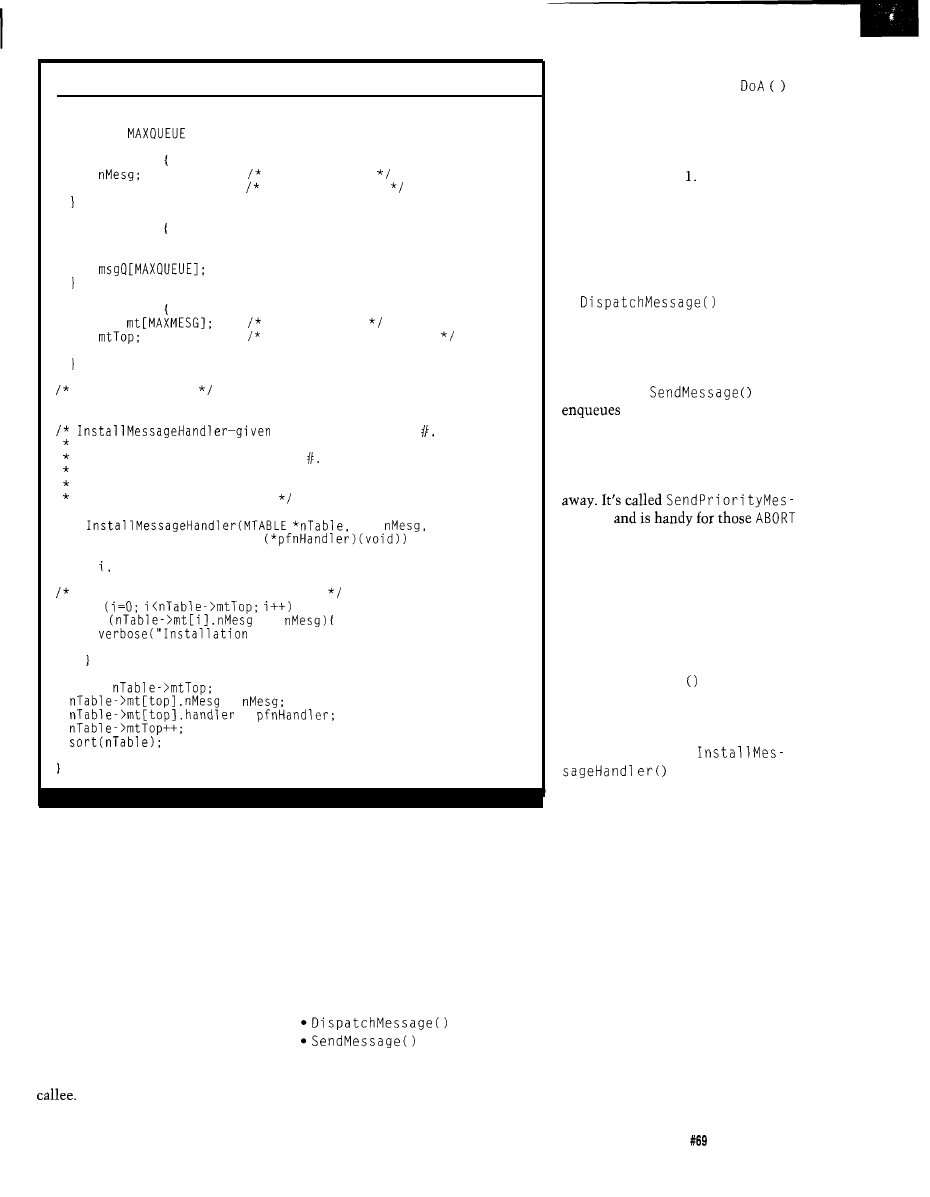
Listing l--The messaging support structures and function handler installation routine take up minimal room.
#define MAXMESG 50
#define
50
typedef struct
int
message number
void (*handler) (void): message function
MESSAGE;
typedef struct
int head;
int tail:
int
QUEUE;
typedef struct
MESSAGE
message table
int
next available position
QUEUE mq;
MTABLE:
global variables
MTABLE tabl:
a table and message
puts function into the message table.
Sorts function table by message
Returns:
0: if message already exists
1: if installed correctly
int
int
void
int top;
search for previous entry on table
for
if
==
Collision")
return 0;
top =
=
=
return 1:
presses, mouse clicks, and serial I/O
can all send messages. Different events
(or sources of events) can send the
same message. Thus, a mouse click
functions the same way as a hot key.
Windows programmers should recog-
nize this mechanism.
The device handler is responsible
for sending messages. A dispatch rou-
tine calls the appropriate subroutine.
To the subroutines, it doesn’t matter
who originally sent the message-they
execute just the same. The messaging
MESSAGE SYSTEM CORE
The concept of this system seems
simple, but building a messaging sys-
tem is simpler. The code examples
here are written in C, but these struc-
tures could be done in any language.
To build a message-based system,
just a few routines are involved:
l
InstallMessageHandlerO
code mediates between the caller and
These and a few other support routines
(see Circuit Cellar BBS) are spun to-
gether. The code doesn’t do anything
very useful (e.g., the message
prints an “A” to the screen). It’s pro-
vided as a skeletal structure on which
to build your program.
InstallMessageHandlerO
can
be found in Listing This routine first
checks to make sure that the message
you’re trying to install doesn’t already
have a handler and returns an error if it
does. If not, the routine simply adds
the ID and function to the message
table, then sorts the table.
isgivenin
Listing 2. This function dequeues a
message, searches the function lookup
table for the message ID, and calls the
appropriate function.
Listing 3’s
simply
the message ID into the
message queue.
Another routine, not reproduced
here, bypasses the message queue and
calls the appropriate routine right
sage0
NOW!
messages.
Although the program is small [it
knows just a few messages), I chose to
keep the message table sorted to re-
duce message-lookup time. This sort is
not critical and could be removed. You
could enhance it by using a binary
search instead of the simple linear
search
D i spat c h
currently uses.
The code also includes an unused
message table, which illustrates the
syntax of a predefined table. Instead of
goingthroughallthe
calls at run time, a
message table can be built at compile
time. This method is easier to read and
debug since it avoids tracking every
InstallMessageHandlerO
call.
At work, I use both a predefined
message table and messages installed
at run time. The dual system means
that I can maintain a simple table of
standard functions that remains the
same for most of my customers, but I
can also add new functions and cus-
tomize them as required.
ENHANCEMENTS
If you look at the program, you’ll
see that it has macro capabilities.
While putting together this article,
I
realized just how simple macros would
Circuit Cellar INK@
Issue
April 1996
39
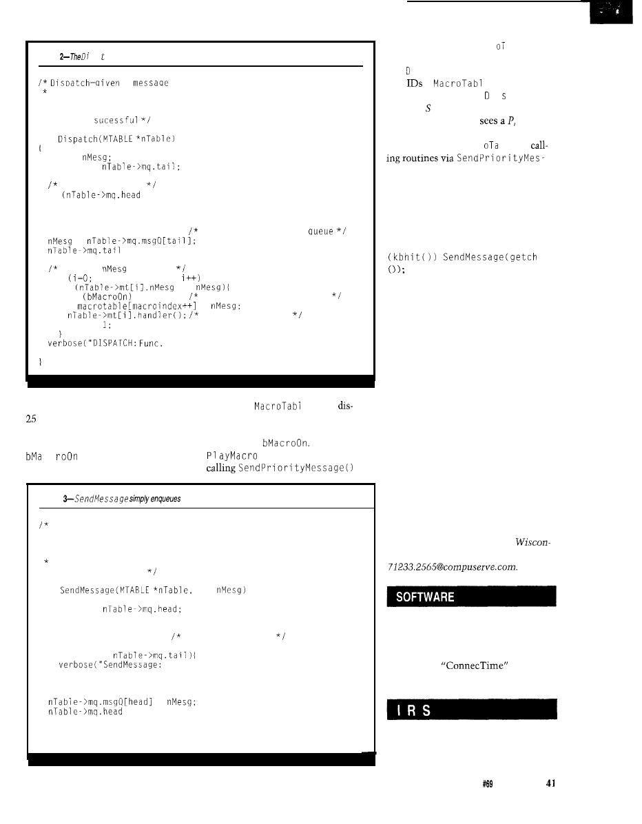
Listing
spa ch
function dequeues a message and calls the associated function.
a
table. calls the function
a t
the head of the queue.
* Returns:
*
0: if message handle not found
*
1: if
int
int i,
int tail =
is queue empty?
if
== tail)
return 0;
tail++;
tail = tail % MAXQUEUE:
wraparound a
=
= tail;
look up
in table
t end of
for
i<nTable->mtTop;
if
==
if
are we recording a macro?
=
call the function
return
not found"):
return 0;
be to implement. The code takes only
array called
e as it
lines. Here’s how it works.
patches. Messages Ma c r o On and Ma c
The D i s pa t c h routine looks at a
r o 0 f f (Record and Stop respectively)
global variable called b Ma c r o 0 n. If
set and reset
The message
c
is set, the routine records
(Play) is a simple for loop,
the message number to an integer
for
Listing
a message.
SendMessage-given a message table and message handle,
*
stuffs the message into the queue.
* Does not check if it's a valid message!
* Returns:
0: message table full
*
1: if successful
int
int
int head =
head++;
head = head % MAXQUEUE; wrap around queue
if (head ==
Table Full"):
return 0;
=
= head:
return 1:
each message stored in Ma c r a b 1 e.
So, if you record a macro by sending
an R, i s pa t c h starts copying mes-
sage
to
e
as
well as
dispatching the message. If i pa t c h
sees an message, it stops recording
macros.If Dispatch
the
P 1 ay Ma c r o routine is called and
cycles through the Mac r
bl e,
sage.
This skeleton could easily be the
base for a simple calculator program.
For instance, draw a calculator on the
screen. A mouse driver would detect
and send button-press messages. A
keyboard driver consisting of i f
would also send messages. A
serial I/O routine could grab characters
from the serial port and send messages
as well. The three different input me-
thods all give the same output.
CONCLUSION
Message-based systems are imple-
mented straightforwardly and are an
easy way to extend a project.
It’s hard to predict a product’s fu-
ture. Designs are often pushed in un-
usual ways. Adding a messaging
structure won’t make a program run
faster, improve the graphics, or jazz up
the user interface of the final product.
What it will do, however, is keep
future expansion readily available and
painless.
q
Pat Baird works as an engineer in the
packaging industry and is an under-
graduate at the University of
sin-Parkside. He may be reached at
Software for this article is available
from the Circuit Cellar BBS, the
Circuit Cellar Web site, and on
Software on Disk for this issue. See
the end of
for down-
loading and ordering information.
413
Very Useful
414 Moderately Useful
415 Not Useful
Circuit Cellar INK@
Issue April 1996
CUSTOMIZABLE EMBEDDED COMPUTER
The
EPC-33
and
EPC-34
single-board computers, based
on the Intel
processor, are unique. They
offer a high level of integration
and graphics options includ-
ing flat-panel and SVGA moni-
tor support and integrated net-
work interfaces. With optional
1 O-Base-T Ethernet, both prod-
ucts can operate as a network
server or network node run-
ning applications remotely. The
units are suitable for medical
instrumentation, telecommuni-
cation equipment, and other
portable, space-conscious en-
vironments.
Users can customize both
units to meet specific needs by
choosing from several options.
Either board can be ordered
with optional
Ethernet
interface and SVGA video
graphics. Otheroptions include
flash and
KB of bat-
tery-backed SRAM. The flash/
SRAM option enables users to
develop diskless systems.
The EPC-33 and EPC-34 use
the Intel DX2 processor run-
ning at 50 MHz and the Intel
DX4 processor running at 100
MHz, respectively. Features
common to both include one
72-pin SIMM socket providing
4, 8, 16, or 32 MB of DRAM;
one RS-232C serial port
one serial port
(COM2) as RS-232 or
485; IEEE
parallel printer port
en-
hanced local-bus IDE harddrive
interface;
compatible
keyboard interface; and a stan-
dard ISA-bus card-edge con-
nector.
The base price for the
33 is $550 and for the EPC-34
is $740, both in quantity. These
prices are for standard con-
figurations and do not include
DRAM, flash, video, or net-
work-interface options.
Corp.
15025 S.W.
Pkwy.
Beaver-ton, OR
(503)
Fax: (503) 646-l 850
EMBEDDED MOUSE SOLUTION
The
offers system integrators and
a turnkey
embedded-mouse solution. This compact, lightweight, ergonomic
device combines a mouse’s functionality with a joystick’s ease of
use to offer both accurate and effortless cursor control.
The
uses a proprietary sensor technology pioneered
by Fujitsu-a magnetic-fielddetection method that uses Hall-effect
devices. The sensor outputs coordinate data according to the
direction and degree of travel of the mobile section. It offers 10”
motion in all directions for positive cursor control and user
feedback. Because the sensors use magnetic technology, they
never wear out. This feature, coupled with a low-profile design that
contains no parts to break or moving elements to collect dust, makes
the
sensor extremely durable.
The
controller IC translates the motion of the sensor
with an Advanced Motion Algorithm. This algorithm, optimized for
the physiological abilities of humans, provides a heightened level
of control. Because little resistance is placed against the user’s
finger, the sensor responds to a feather touch, making exact cursor
positioning easy to attain. The IC provides autoselectable RS-232
and
output and supports both the IBM and Microsoft
button and Logitech’s three-button mouse protocols. Various con-
figurations are available for off-the-shelf design implementation.
The
assembly, including the sensor, IC board, and
driver is available from USAR Systems. An evaluation kit, compris-
ing the assembly, cables, and documentation, sells for $95. A User
Input Device
is also available.
Systems
568 Broadway
l
New
York, NY
(212)
l
Fax: (2 12) 226-32 15
44
CIRCUIT CELLAR INK APRIL 1996
SING
COM
co
CPU:
SBC 1
expar
5 x 8 6
intern
floatir
cycle]
a
cessir
the Ic
make
expa
local
spea
P C /
max
The
C
104
is
tion
1
war
for
S I N G L E - B O A R D 5 x 8 6
C O M P U T E R
Computer Dynamics has re-
leased a pair of single-board
computers based on the 5x86
CPU: the PC/l 04-expandable
and the
expandable SBC-586. The
5x86 processor offers a 64-bit
internal data path, an
floating-point unit, branch pre-
diction (which allows multiple
instructions in a single clock
cycle), and speeds faster than
a 75-MHz Pentium. This pro-
cessing power, combined with
the local bus video controller,
makes each board a GUI engine ideal for driving flat panel
displays and running demanding software.
Pentium-class performance creates an unequalled PC/l
expandable platform for graphics-intensive applications. Data
never slows down, from CPU to video and out to the hard drive. The
local bus IDE port supports up to two hard drives, each up to
8.4 GB. The
6.5” board also features up to 32 MB of DRAM,
speaker and keyboard interfaces, a real-time clock, and the
to
interface. The
is rated at
operates at
V only, and consumes less than 10 W.
The SBC-586 board local-bus video controller runs at 32 bits for
maximum throughput and features built-in Windows accelerators.
The
7.75” board drives XGA
x 768) color
VGA color
or
passive matrix color
in 64,000 colors. Up
to 64 MB of DRAM is offered
Three sockets
port 5
EPROMs, 5
and 256-KB flash
memory for a total RAM and
ROM capacity of
MB.
The SBC-586 has an IDE
hard-disk controller which sup-
ports up to two 8.4-GB hard
disks. Other SBC-586 features
include two COM ports, a
printer port, watchdog timer, real-time clock, speaker and key-
board interfaces, and a standard Phoenix BIOS. An ISA PC bus
connector and an SBX connector are included for expansion. This
board is also rated at 0-70°C and draws 9.7 W.
Pricing for the
is
$1520
and the SBC-586 is
$1620 (in quantities of 100,
DRAM).
Computer Dynamics
7640 Pelham Rd.
l
Greenville, SC 29615
(864)
l
Fax: (864) 675-0106
PC/ 104
LCD CONTROLLER
Communication and Display Systems has introduced
104
controller to interface LCD flat panels to PC/l 04 embedded
systems. The controller is compatible with both color and mono-
chrome passive-matrix LCD panels from 320 x 240 to 640 x 480
resolution. An embedded PC/l 04 system with a flat-panel display
is useful in industrial, commercial, scientific, and medical applica-
tions.
The VGA-l 04 features a standard PC/l 04 format and hard-
ware VGA compatibility. Colors are converted to 64 gray shades
for monochrome panels and 4096 colors for passive, dual-scan
color panels. The board includes 5
display memory, vertical
centering, and
generation of all display voltages. It
measures 3.775“ x 3.550” and draws less than 180
at 5 V.
Communication Display Systems, Inc.
194-22 Morris Ave.
l
Holtsville, NY 11742
(5 16)
1143
l
Fax: (5 16)
1496
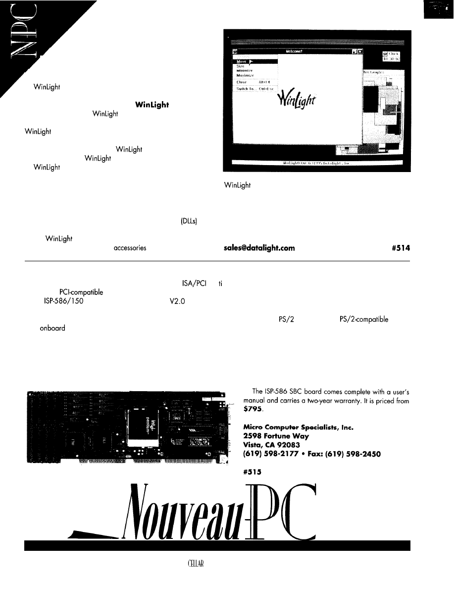
E M B E D D E D O P E R A T I N G S Y S T E M
Winlight,
a Windows-like operating system,
.
is designed specifically for embedded and mobile
systems. It enables developers to use standard Windows
desktop development tools for creating applications that
operate with less than 256 KB of code space.
supports only the calls needed for an embedded
system, so it requires smaller ROM and RAM. Source code for
device drivers is included in the
Software
Developer’s Kit, so
can be customized for nonstand-
ard hardware such as unusual screen sizes, shapes, and types. The
SDK also includes software utilities to create a ROM disk
for placing applications and the operating system in ROM. It can
even run the code portions of
and most applications
directly out of ROM.
source code is also available.
features a Graphical User Interface (GUI) and coop-
erative multitasking, and runs in protected mode like Windows.
The GUI enables developers to create user-friendly screens with
pop-up menus, buttons, and windows. An end user selects from
among buttons representing valid selections on each screen, rather
than having to use a keyboard and know proper syntax. It also
supports Windowscompatible Dynamic Link Libraries
and
resources that enable easy application customization.
The
Software Developer’s Kit sells for $595. The kit
provides the software tools and
necessary to configure
for various hardware environments and includes a
certificate for 20 duplication licenses. License fees vary from $12
per copy for 500 to $6 per copy for 10,000.
Datalight
188
10 59th Ave. NE
l
Arlington, WA 98223
(360) 435-8086
l
Fax: (360) 435-0253
PENTIUM-BASED CPU BOARD
Operating at speeds up to 150 MHz, the ISP-586
Pen rum board combines a full-featured passive-backplane CPU with a
high-speed
bus and a PC/l 04 expansion port. This mix makes it ideal for high-speed embedded applications.
The
MHz performs at a Landmark
rating of 863 MHz. The PCI expansion bus is compatible with the PCI Industrial
Computer Manufacturers Group (PICMG) specification and supports up to four PCI master peripheral boards. The board includes two
serial ports, a bidirectional parallel port, a dual floppy-disk port, an IDE hard-disk port, a
keyboard port,
mouse
port,
speaker, watchdog timer, and up to 128 MB of DRAM.
In addition, each board has a standard PC/l 04 expansion port for adding optional boards such as an EPROM/RAM disk-emulator
board, video controller, or digital I/O. Since the ISP-586 was designed for embedded and industrial applications, the BIOS boots without
either a keyboard or monitor.
The watchdog timer makes the board ideally suited for controlling critical processes where unattended operation is essential. It can
be programmed to generate a nonmaskable interrupt or system reset in the event of an I/O timeout delay or external failure. The timeout
delay is adjustable from 1 to 220 s.
46
CIRCUIT
INK APRIL 1996
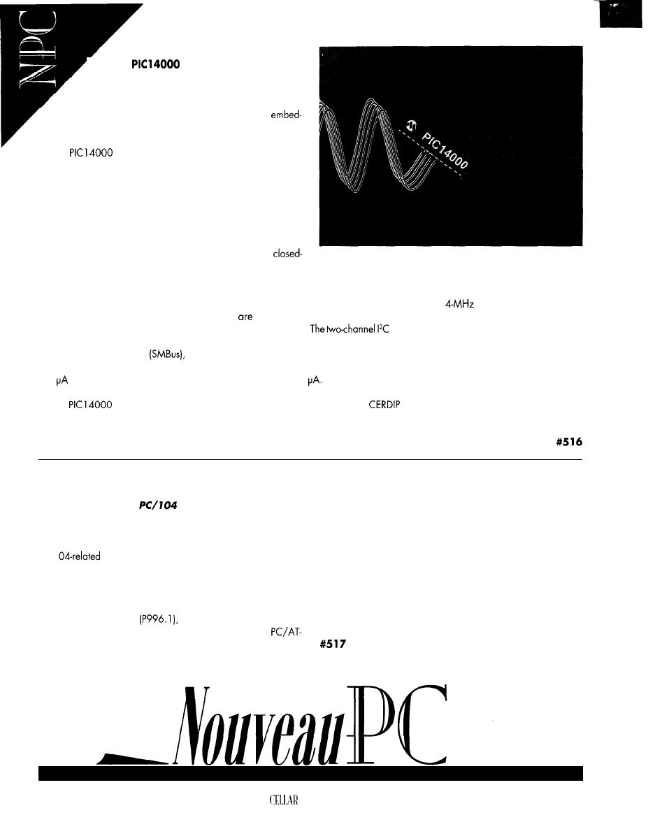
PROGRAMMABLE CONTROLLER
,
The
mixed-signal controller targets
a variety of applications where analog signals are
measured and digital control and communications are
Implemented. Typical applications include smart batteries,
battery chargers, portable computers, instrumentation,
ded temperature sensors, and systems needing high-resolution
data acquisition and processing.
The
offers 4-KB x 14 on-chip EPROM program
memory and 192 bytes RAM based on an 8-bit RISC core, enabling
it to support algorithmic-intensive calculations at up to 5 MIPS.
Other features are 35 single-word instructions, up to 20-MHz
operating speed, 6 internal and 5 external interrupt sources, 11
interrupts, 8 levels of hardware stack, and 38 special-function
hardware registers.
The A/D and D/A converters measure and generate analog
signals enabling the design of inexpensive, single-chip,
loop systems requiring few external components. A slope A/D
converter offers programmable resolution up to 16 bits, enabling high-precision measurement of real-world signals. Two multirange D/A
converters can be used for precise control applications such as charging batteries. To reduce the need for external components, the device
features an on-chip low-voltage detector, temperature sensor, voltage-regulator control, and internal
clock oscillator.
Twenty I/O pins with individual direction control
available for interfacing with displays, interrupts, data input, and communications
interfaces to supportanythree-wire, two-wire, or single-wire interfaces.
port enables high-speed serial communications
between other microcontrollers as well as data storage with nonvolatile memories. The PIC 14000 supports the ACCESS.bus, Intel/Duracell
Systems Management Bus
and Standard Battery Data standards.
To address low-power concerns, particularly in portable systems, the chip supports both a Sleep mode that dissipates no more than
200
and a new Hibernate mode that dissipates no more than 5
The device can be programmed to wake from Sleep on sensing
a specific level of current flow, within a range of current flow, and outside a given range.
The
sells for $6.85 in quantity and is available in DIP, SSOP, and
packages.
Microchip Technology, Inc.
2355 W. Chandler Blvd.
l
Chandler, AZ 85224-6199
l
(602) 786-7200
l
Fax: (602) 899-9210
PC/l 04 RESOURCE GUIDE
The PC/l 04 Consortium announces the Eighth Edition (Novem-
ber 1995) of its popular
Resource Guide.
Like its
predecessors, the 200-page booklet is available free to engineers
and companies developing embedded systems. It includes an
overview of the PC/l 04 standard, a cross-reference of available
PC/l
products and functions, and product listings from
over 130 of the Consortium’s member companies which describe
the companies’ PC/l 04 modules and related boards, peripherals,
and software.
The PC/l 04 standard, which has also become the basis of a
new IEEE draft standard
defines a compact, self-stack-
ing, modular form factor for embedding IBM PC and
compatible system functions within embedded microcomputer
applications. The PC/l 04 modules’ small size (3.6” x 3.8”) and
low-power requirements (typically l-2 W per module) make them
ideally
suited to embedded-control applications. Such applications
include vending machines, test equipment, medical instruments,
communications devices, vehicular systems, data loggers, and
industrial control subsystems.
PC/ 104 Consortium
P.O. Box 4303
Mountain View, CA 94040
(4 15) 903-8304
Fax: (415) 967-0995
48
CIRCUIT
INK APRIL 1996
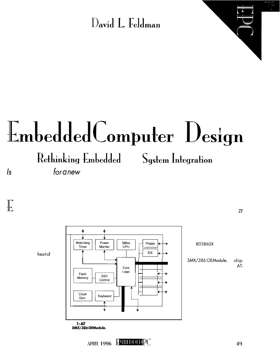
PC
there
room
form factor in the embedded systems market? New
chip-based plug-in modules with ISA compatibility offer designers another way
to speed embedded designs to market.
mbedded systems are so widely used
An option that increases the integration
computers is chip-level integration.
in the appliances of everyday life that we
of embedded systems and single-board
Microsystems recently introduced the
largely take them for granted.
From the microwave ovens, cof-
fee makers, cellular telephones,
and fax machines to the elec-
tronic systems of complex medi-
cal instruments, embedded ap-
plications form the
many
consumer products.
Nonetheless, designing a
new embedded system poses
great challenges to system inte-
grators. The search for smaller,
faster, and less expensive prod-
ucts remains critical.
While most embedded-PC
vendors seek higher levels of
integration by redesigning the
form factors of board-level prod-
ucts, others rethink the way
a
PC
is integrated into an embedded
system.
DRAM
Bus
Parallel
Serial 1
Serial 2
ISA Bus Speaker
Figure
the functions of a PC/AT motherboard are integrated into
the
Embedded DOS delivers the C: prompt when
the system is powered up.
Single-Device Personal Com-
puter (SDPC), a line of ultramin-
iature, PC-compatible modules.
The modules incorporate an
Intel
microprocessor
and all associated logic chips in
a single module. Thecompany’s
a
like module, complete with
compatible BIOS, embedded
DOS, and a PC ISA bus stan-
dard interface, works well in a
broad range of embedded sys-
tems requiring PC compatibility.
S P E E D I N G
D E V E L O P M E N T
Whilecreating smaller, faster,
cheaper, and lighter products,
designers are looking for the
best and fastest way to get their
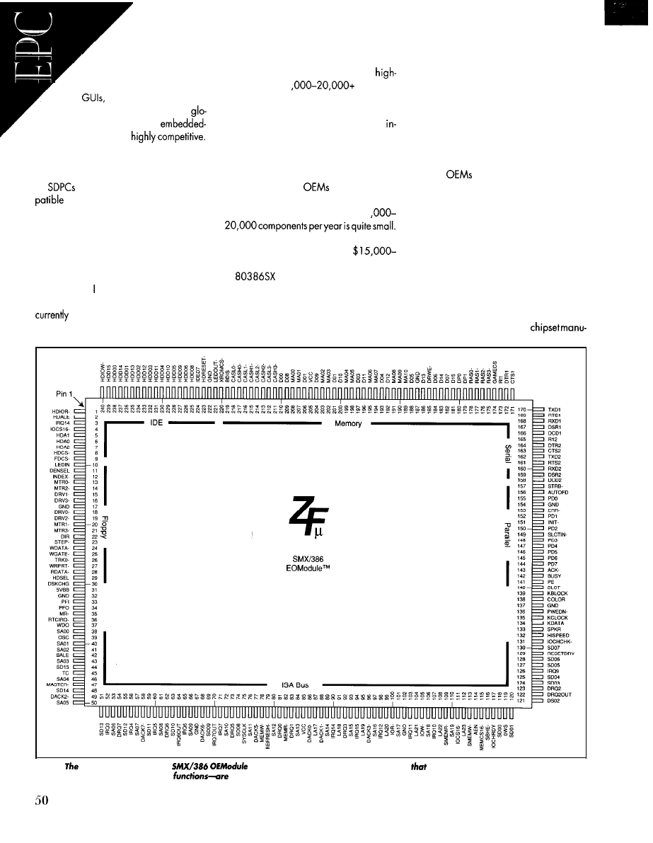
embedded products to
market.
With its readily available
and cost-effective development
tools,
and operating systems,
the x86 architecture has achieved
bal dominance. As a result, the
PC market has become
There’s a need to provide solutions other
than the standard board-level offerings
currently available.
The obvious advantages are that
house design typically offers the lowest
hardware cost and greatest integration.
You therefore gain the smallest, most reli-
able overall solution.
provide complete PC/AT-corn-
However, these
have significant
subsystems in a semiconductor-like
obstacles to overcome with in-house de-
module that provide CPU, I/O, and flash
sign. To semiconductor suppliers, 1
disk functions based on Intel’s x86 archi-
tecture. They’re application independent
At today’s prices, Intel or Advanced Micro
computer subsystems that can be incorpo-
Devices stand to gain only
rated directly into a customer’s proprietary
$150,000 of annual revenue from the sale
circuitry.
of
processors to such accounts.
But, before elaborate about the SDPC,
let’s check out what problems engineers
experience
in designing and build-
ing products that are PC compatible.
For the large chip suppliers, the amount
of revenue is too low to merit the sales and
support costs. Thus, such customers are
rarely given direct attention. Instead, they
I N - H O U S E D E S I G N
This approach is most common when
product volumes are in the mid- to
level range (1
units per
year). However, designing from scratch
has both advantages and disadvantages.
are typically pushed through an industrial
distributor.
Component pricing from industrial dis-
tributors is quite high compared to direct,
higher-volume pricing. Distribution mar-
gins rarely support the high level of techni-
cal support required by the OEM’s engi-
neering staff. As a result, consultants are
frequently used, which drives development
costs even higher.
The
in this segment are thus
caught in the middle. Board-level systems
cannot deliver the best solution in terms of
cost, size, or reliability. And, semiconduc-
tor manufacturers don’t want to deal with
them directly since their business potential
is simply too small.
In addition, in-house design, which is
based on discrete components, is particu-
larly vulnerable since any one component
designed into the board could become
obsolete. As the desktop market leaves
older technologies behind,
Top View
Figure 2:
pin assignments on the
enable designers to locate the module so
connections to peripherals-mars rtomge,
memory, video, and other external
convenient and simple.
CIRCUIT CELLAR INK APRIL 1996
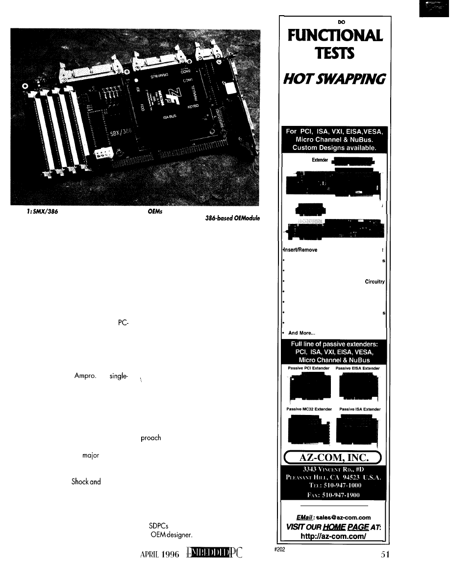
Photo
plug-in development boards offer
the fastest possible time to market.
Developers gain an easy development environment that includes the Intel
on a PC card along with PC AT-compatible BIOS and embedded DOS.
facturers often discard components which
n o l o n g e r h a v e m a s s - c o n s u m e r a p p e a l .
T h i s v u l n e r a b i l i t y p o t e n t i a l l y j e o p a r d i z e s
an entire project. The greater the
n
u
m
b
e
r
o
f
discrete components in the design, the
higher this risk becomes.
Finally, board solutions involve the on-
going cost of procurement and inventory
management of the up to 100 individual
components required to produce the
compatible portion of an in-house design.
O F F - T H E - S H E L F B O A R D S
Engineers can also use an off-theshelf,
board-level computer from companies like
Megatel, Radisys, or
The
board computer, connected via a series of
cables, then becomes the engine driving
the OEM’s proprietary electronics.
Although these boards have found wide-
spread use in applications requiring 1,000
or fewer boards per year, they don’t satisfy
the requirements of higher-volume applica-
tions where size, power consumption, or
harsh environments are a
concern.
The main drawback of this type of
embedded solution lies in the inherent
decrease in reliability.
vibration
can cause the interconnecting cables and
mounting hardware to loosen.
Additionally, many board-level suppli-
ers build bus-oriented products, requiring
large backplanes and card cages. The
form factors of these products are typically
too large and costly for most high-volume
applications.
The business structures of these suppli-
ers are oriented toward the small to me-
dium OEM and industrial end-user markets
(100-l ,000 units). The products are built
in relatively small volumes and carry rela-
tively high price tags (e.g., a $100,000
anesthesiology machine).
The higher cost of these solutions and
the additional overhead of power, space,
and assembly time limit the OEM designer
to use these solutions in similar low-volume,
high-end products.
S U B S Y S T E M I N T E G R A T I O N
E ngineers can also integrate a sub-
system with a single-board computer in
their equipment either with their own team
or an outside VAR doing the integration.
However, this is just a bolt-on approach.
The advantage of the subsystem ap
is that the subsystem becomes a
“standard” unit that can be easily inte-
grated into additional projects. It also rep-
resents a convenient method for easy field
service swap-out.
The penalties of large size and higher
cost remain, thus again limiting solutions to
high-end, low-volume applications.
S I N G L E D E V I C E P C
represent a new alternative for
the
The modules offer many
IF
YOU
YOU NEED
ELECTRONIC
EXTENDERS
Electronic ISA
I
PC Mini Extender
Electronic PCI Extender
PCI Mini Extender
Cards With PC Power On!
Save Time Testing And Developing Card
Save Wear On Your PC From Rebooting
Adjustable Overcurrent Sensing
NO Fuses, All Electronic For Reliability
Single Switch Operation W/Auto RESET
Optional Software Control Of All Feature
Breadboard Area For Custom Circuitry
24-Hour
Fax on Demand:
51
O-947-1 000 Ext.7
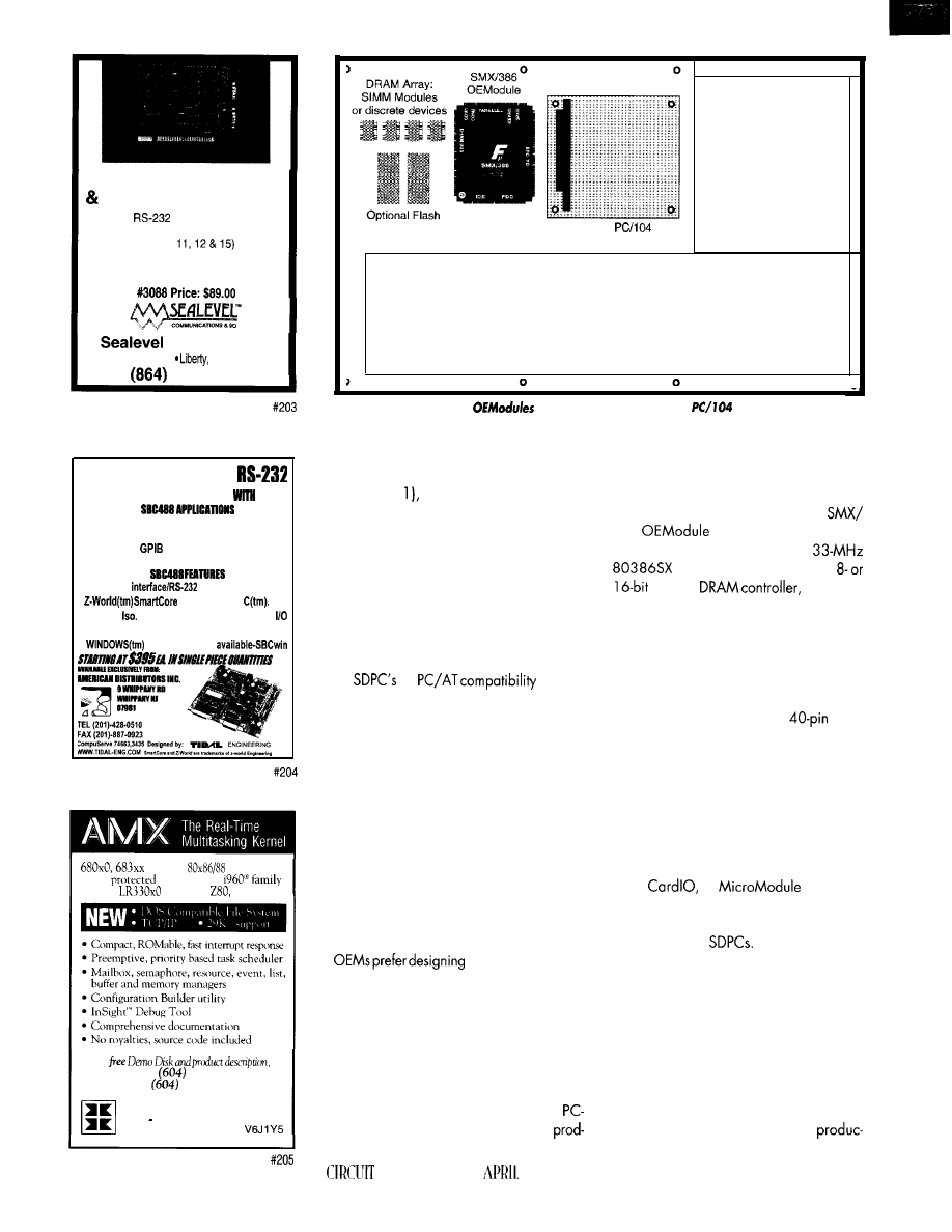
Enhanced Windows
OS/2 Communications
l
Two
Ports
l
Independently Selectable Address
l
IRQ(2-5, 10,
l
16550 UART Standard
l
16 Bit Addressing
l
Free Technical Support
Part
Systems, Inc.
P.O. Box
830
SC 29657
8 4 3 - 4 3 4 3
SBCIEEE-488 AND
SINGLE BOARD COMPUTER
C
Why tie up a PC/Workstation? The SBC488 is a
stand alone test controller,
an OEM
8 RS-232 interface and
an RS-232 to IEEE 488 converter.
. IEEE 488.2
interface.
.
with DYNAMIC
. Optically
12 Bit D/A, A/D and 24 Bit Digital
. Source code available for OEM applications.
l
control program
real
mode
80386
mode
R3000,
HD64180
For a
Phone:
734-2796
Fax:
734-8114
KADAK Products Ltd.
206
1847 West Broadway
Vancouver, BC, Canada
52
Proprietary Electronics
Disk expansion
Optional
peripheral expansion
Proprietary Electronics
Figure
3:
PC-compatible
can control a wide array of
peripherals. Designers
therefore not only reduce overall system costs but also speed up their time-to-market.
benefits of an in-house design. As a dis-
crete component in a proprietary design
(see Photo
the end product has a high
level of integration, reduced component
count, and increased reliability.
The attendant headaches
of developing
or licensing and modifying a BIOS and
operating system areeliminated.
Also, since
everything is within the one chip, the pro-
curement and inventory of numerous dis-
crete components becomes minimal.
Using this approach, engineers can use
an
full
to build
cost-effectiveembedded systems.Theygain
the benefits of the huge base of PC software
and hardware while dramatically reduc-
ing development overhead.
For instance, when a company builds a
medical device, such as a blood analyzer,
that is PC compatible, the challenge is not
to build a better PC, but a better blood
analyzer. By using an SDPC with an al-
ready developed BIOS, blood analysis,
not PC BIOS implementation, gets greater
attention. The end result: a product is intro-
duced more quickly and at lower cost.
Rather than outsourcing portions, most
productscompletely
because it’s expedient and volumes are
low enough to handle internally. But, with
higher product volumes, other problems
come such as reliability and testing. These
issues can make full in-house designs less
attractive or unfeasible.
For those companies, an SDPC repre-
sents a fast way to incorporate a fully
compatible system controller into their
CELLAR INK
1996
uct.
The module represents the lowest pos-
sible development risk and greatest reduc-
tion in time-to-market.
As you can see in Figure 1, the
386
includes all standard
motherboard functions. It has a
CPU, full PC core logic, full
ISA bus,
serial and
parallel I/O, floppy and IDE disk control-
lers, embedded AT-compatible BIOS, and
256 KB of user-available flash disk. Em-
bedded DOS delivers the C: prompt when
the system is switched on.
In Figure 2, you can see that the module
provides 240 pins with a full
inter-
face to a standard IDE hard disk drive. The
pins interfacing to the ISA bus are conve-
niently located to ease board layout.
The common denominator for the
multichip modules appearing in the em-
bedded market is the attempt to provide
close to PC functionality in a single device.
ZF Microsystems OEModules, S-MOS Sys-
tems
or
Systems’
Northstar series of Pentium processor mod-
ules are all examples of products that could
be classified as
Although each of these products targets
a different segment of the embedded mar-
ket, they all bring a high level of integra-
tion. The embedded designer is able to
shorten development times and eliminate
the overhead associated with incorporat-
ing a single-board computer into an em-
bedded application.
These SDPC modules represent a layer
of functionality ideal for midrange
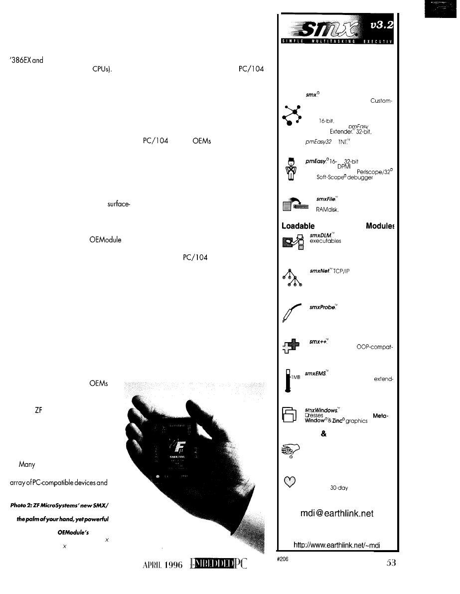
tion volume levels. They’re optimally suited
for the middle ground between high-vol-
ume embedded markets such as Intel’s
the lower-volumesingle-board
computer (including PC/l 04
Nota-
bly, with lower volume, additional cabling
and hardware mounting are acceptable
alternatives to designing from scratch.
The most significant advantage of the
SDPC’s component-like construction ap-
pears when designing for harsh environ-
ments. In a stressful environment, the issues
of mounting hardware and system size rise
to the forefront of system design decisions.
The integrated SDPC fits an entire AT
motherboard into a space that’s roughly
equivalent to that required for two Intel
486DX chips. Designed for embedded
systems, it needs minimal external compo-
nents. The chip-like design of the
mount device ideally suits SDPCs to de
signs demanding low power consumption,
high reliability, and small product size.
As Photo 2 illustrates, an
fits
easily in a hand. While many single-board
computers of equivalent technology require
a 5.75”
x
8” footprint (46 square inches),
this module only takes up 2.2” x 3” or 6.6
square inches. It replaces many propri-
etary solutions that add more cables and
wiring to embedded systems.
By SDPCs using the industry-standard
PC/AT ISA bus, designers can leverage the
most cost-effective and widely available
selection of hardware and software. This
flexibility allows product designers to start
with a proven architecture that is widely
serviced and takes advantage of low-com-
ponent prices.
With PC compatibility,
have access to many cost-effective
development tools and operating
systems. Microsystems also pro-
vides CAD files so designers can
integrate the module into board
layouts like any other chip.
ISA AND INTEGRATION
designers looking for ease
of integration want to use the vast
386 chip module is tiny enough to fit
in
enough to run many embedded PC
applications. The
overall
footprint measures a scant 2.344”
3.125” (59.54 mm 79.88 mm).
peripheral products available for the ISA
standard.
The SDPC’s fully compatible ISA bus
interface makes this possible. By adding
either an ISA PC-type slot or a
connector for expansion, hundreds of stan-
dard PC peripherals are available. The
OEM can then enjoy the best of both
worlds: proprietary in-house design ben-
efits and industry-standard peripherals.
In a sense, SDPC is the step after
PC/l 04. At the time of its conception,
helped
bring highly inte-
grated embedded devices to market as
quickly as possible. Now backed by about
130 member companies in the PC/l 04
Consortium, the standard substantially re-
duces development costs, risks, and devel-
opment time.
Embedded-systems designers also have
widespread use of PC standard hardware
and software. Components for this widely
available architecture are more economi-
cal than for traditional architectures, such
as STD, VME, and Multibus.
However,
has some inherent
limitations as a CPU platform. As embed-
ded-PC system software becomes more
complex and requires greater amounts of
memory, an embedded CPU design be-
comes less cost-effective within the con-
straints of the PC/l 04 board outline.
By incorporating an SDPC directlywithin
a proprietary design and adding a PC/l 04
connector for expansion, overall system
cost is greatly reduced without sacrificing
the benefits of the wide variety of PC/ 104
peripherals available (see Figure 3).
Complete
x86 Solution!
Multitasking in Real and
Protected Mode
Full-featured, high-perform-
ance, preemptive kernel.
ized to x86 processors. Ideal for
demanding applications. Real
mode works stand-alone or with
DOS.
segmented protected
mode works with
16 or
286 I DOS
flat
protected mode works with
or
Protected Mode Environment
or
protected
mode entry,
services,
application loaders,
and
support
DOS-Compatible File System
Full-featured file
manager. IDE, floppy, flash,
and PCMCIA drivers
available.
Dynamically
Runs independent
as tasks which may
be downloaded or loaded from
disk. floppy, flash, etc.
Networking
stack. Fast UDP.
Packet driver interface. Ethernet,
SLIP, and PPP drivers. FTP, SNMP,
NFS. Net server, other protocols
Task-Level Debugging
Provides tracing and
symbolic debugging. Works with
or without code debuggers.
Local or remote operation.
C++
Classes
Class library built upon
smx. Provides fully
ible kernel interface.
Extended Memory, Real Mode
Allows copying data
between real memory and
0
ed memory buffers or accessing
extended memory via a window.
User Interface
Text windowing.
up user interfaces.
support.
Low Cost Easy to Use
Royalty-free licenses. Supports
common, low-cost C compilers,
debuggers, and locators. Great
manuals, Source code available
Reliable
On the market 7 years. 100’s of
applications. Extensive error
checking.
free trial.
l-800-366-2491
MICRO DIGITAL, INC
fax 714-891-2363
intn’l 714-373-6862
ZF MICROSYSTEMS’
Key features:
l
Chip-like design in very small form factor (2.2” x 3”)
l
PC compatibility
l
Built-in AT-compatible BIOS and embedded DOS PC/l 04 standard interface
l
Fast, easy development environment
Body Size:
l
2.20” x 3.00” x 0.450”
Overall Footprint:
l
3.125”
leads:
l
240 (50 x 70) gull wing pins
at 0.030”
l
See Figure 2
Power requirement:
l
V
at 750
Operating environment:
l
14°F to 158°F
l
-10°C to
l
relative humidity
(noncondensing)
Storage temperature:
l
-67°F to 185°F
l
-55°C to
Weight:
l
5 oz.
l
A
WAY?
Development done on a PC/AT system
Off-the-shelf hardware and development
is easily transferred to the embedded
systems give embedded system designers
tern with little or no modification. In the
flexibility.
Theypotentiallysave
case of
customers receive not
development time and purchasing costs.
just an AT BIOS and embedded DOS for
development, but also a CAD file contain-
ing
component outline for the module.
Compact, rugged, easy. Perhaps it’s
time to seek another solution.
David Feldman is president and chief
executive officer of
Microsystems, a
startup embedded systems developer
founded in April 1995. Dave formerly
served as the founder and former chief
executive
Computers, the creator
of the PC/I 04
concept,
and
has
more than
25 years of experience in business man-
agement and the embedded systems mar-
ket. He may be reached at
zfmicro.com.
CONTACT
($260
in
1 0 0 0 s )
Microsystems, Inc.
1052
ct.
Palo Alto, CA 94303
(415)
Fox: (415)
I R S
4
16 Very Useful
4 1 17
Moderately Useful
4 18 Not Useful
$129.95 FOR A FULL FEATURED SINGLE
BOARD
COMPUTER FROM THE COMPANY THATS BEEN
BUILDING SBC
5. THIS BOARD
COMES READY
FEATURING TH
80535 PROCE
W H I C H I S
8051 C O D E
COMPATIBLE.
A KEYPAD
AND AN LCD
DISPLAY AND YOU HAVE
A STAND ALONE CONTROLLER WITH
ANALOG AND DIGITAL I/O. OTHER FEATURES INCLUDE:
UP TO 24 PROGRAMMABLE DIGITAL I/O LINES
8 CHANNELS OF FAST
10 BIT A/D
4 CHANNEL, 8 BIT D/A
UP TO
BIT TIMER/COUNTERS WITH PWM
l
UP TO 3
SERIAL PORTS
BACKLIT CAPABLE LCD INTERFACE
l
OPTIONAL 16 KEY KEYPAD INTERFACE
192K OF MEMORY SPACE, 64K INCLUDED
8051 ASSEMBLER MONITOR
BASIC OPT.
inc.
F a x
P.O. BOX
2042. CARBONDALE. IL 62902
CIRCUIT CELLAR INK
Net-Port is a corn
tern in a
nication line drivers.
no programming. A
l
RS422, and RS-485 at
bps to 115 kbps
l
Sixteen parallel I/O lines and bus
l
I-channel. B-bit
(Net-Port
l
P-channel,
ADC and
DAC (Net-Port
l
PWM output:
to 3.5
cycle
l
Simple ASCII command set, requires no programming!
l
High-performance, built-in functions: parallel I/O buffering. LCD and keypad
control, analog data averaging, data logging
l
Sixteen-character ID allows hundreds of Net-Ports
l
Small size, encapsulated construction
l
Wide power supply input range
carrier board w/power supply
‘rices do not include
subject to change
4 Park Street
l
Vernon, CT
871-6170 Fax
1996
an Building
Harsh
For computers to work in harsh environments, extra care must go into the
design and manufacturing of the systems.
characterizes harsh
environments, examining what design criteria are needed
for
specific
stresses.
e
W I
e y accepted Wintel PC architec-
ture is increasingly found in inhospitable
habitats. Unfortunately, the hardware de
signers of PC chips never intended their
products to be operated in anything but
comfortable human habitats.
So, how does one design and manufac-
ture PC-compatible computers that operate
reliably in environments like vehicles, in-
dustrial plants, and outdoors?
Designing electronic systems for harsh
environments is well understood in aero-
space applications. The Department of
Defense (D
O
D), NASA, and commercial
airplane manufacturers have designed
customized computers. and mechanical
structures with operating lifetimes of over
20 years.
Besides the clever packaging of elec-
tronic and mechanical components, they
use components specifically designed for
extreme environments. As a result, the
component technology used in aerospace
systems has generally lagged commercial
computer technology by 3-5 years.
The effect of harsh environments on
electronic components is also reasonably
well understood. Based on this informa-
tion,
and NASA have developed
qualification procedures and approved
parts lists.
These approved lists are organized
according to different harshness catego-
ries for a variety of environmental condi-
tions. Some parts survive the radiation
environments of low-earth orbit, some en-
dure atmospheric flight, and so on.
Most harsh environments are also char-
acterized and defined in accordance with
environmental design standards. (There
are many such standards maintained by
standards organizations worldwide.) In
addition many companies, particularly
vehicle manufacturers, develop their own
proprietary environmental specifications.
After looking at the characteristics of
harsh environments and their affects on
components,
provide some techniques
for designing and developing PCs to oper-
ate in harsh environments.
C H A R A C T E R I Z I N G H A R S H
E N V I R O N M E N T S
Computers are used in many harsh
environments: industrial plants, ground
vehicles (on and off road), airborne ve-
hicles, geophysical, traffic monitoring, and
so on. Each of these environments has its
own thermal, vibration, shock, humidity,
power, and
characteristics.
Computers have to be designed and
manufactured to operate reliably in these
adverse conditions. To do so, we need to
understand the effect of extreme conditions
on rugged computers. Characterizing and
then simulating these extreme conditions is
required to design and test a rugged com-
puter for proper operation in the field.
Let me spend some time characterizing
the environmental conditions that rugged
computers need to operate in.
Temperature extremes range from the
cold of Canada to the heat of Saudi Arabia
and are caused by extreme ambient tem-
peratures. These extremes are also man-
made. For example, there’s the cold of a
5 5
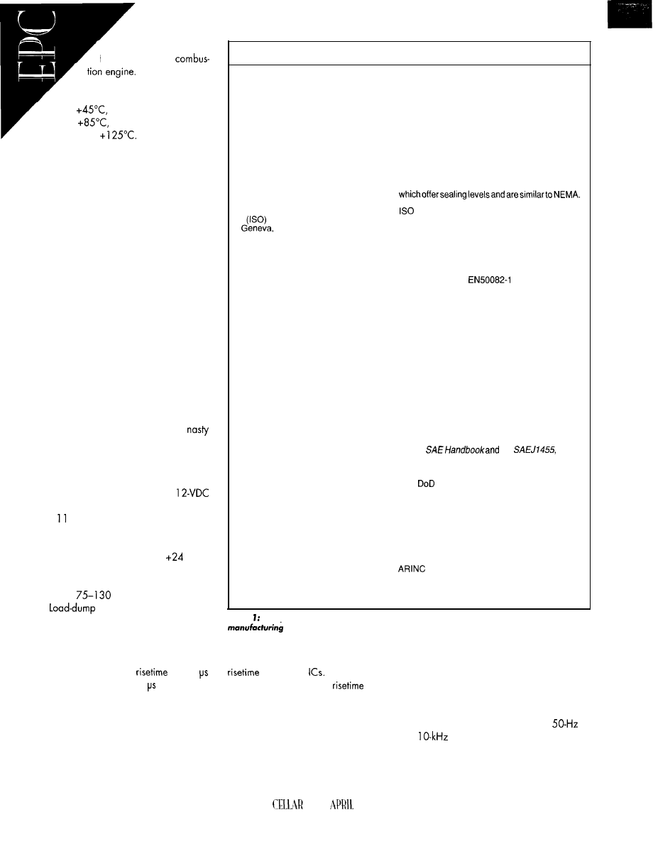
food freezer or the heat
from an internal
Generally, commercial prod-
ucts are designed to operate from
0°C to
industrial products from
-40°C to
and military avionics
from -55°C to
However, there
are as many exceptions to these standards
as there are computers using them. Nota-
bly, for most applications, the industrial
temperature range is sufficient.
All computers, rugged or not, are sub-
jected to shipping-and-handling shock dur-
ing the trip from their place of manufacture
to the place of operation. Computers in
environments with rotating or translating
machineryaresubiected to additional shock
and vibration during their operational life.
The severity of the shock and vibration
depends on the role of the machine and its
condition. A computer mounted on an
injection-molding machine is subjected to
repeated shocks as the mold iscompressed.
A forklift-mounted computer, on the other
hand, experiencescontinuousvibration and
occasional collision shock.
Barring lightning surges, AC power
from national power grids is generally
pretty stable. On vehicles, however, DC
and AC power is noisy and full of
transients and voltage surges. Rugged com-
puters must deal with power fluctuations
without data loss and their power supplies
must survive the power aberrations.
In a heavy-duty vehicle with a
power system, the power normally varies
from
to 16 VDC and dips down to as
low as 4.5-6 VDC during a cold crank
(engine starting at -40°C). Jump starts can
cause voltage surges of -12 to
VDC.
Voltage-regulator failure causes the battery
electrolyte to boil off with resulting voltage
surges of
VDC.
transients occur when the
vehicle’s alternator current load abruptly
reduces. This fallout happens, for example,
when headlights are switched off. This
simple action can cause a voltage spike of
up to 150 VDC with a
of 100
and a decay time of 100 to 4.5 s.
Rugged PCs are subject to electrostatic
shocks similar to desktop computers. Hu-
mans generate charges in normal daily
activities of more than 10,000 V. When
we touch a computer, the faceplate, or an
I/O connector, the electrostatic discharge
(ESD) can damage the computer.
56
Standards Organization
Description
National Electrical Manufacturers
Association (NEMA)
Washington, DC
International Electrotechnical
Commission (IEC)
Geneva, Switzerland
International Standards Organization
Switzerland
European Commission (EC)
Brussels, Belgium
Electronic Industries Association (EIA)
EIA defines electrical and communications
Washington, DC
standards that apply to rugged computers.
Institute of Electrical and Electronics
Engineers (IEEE)
Piscataway, NJ
IEEE defines electrical and communications
standards that apply to rugged computers.
American National Standards Institute
New York, NY
ANSI defines electrical and communications
standards that apply to rugged computers.
Federal Communication Commission
(FCC)
Washington, DC
FCC outlines manystandardsfor RF compatibility.
Part 1.5, subpart B defines emission limits for
unintentional radiators such as rugged computers.
Class A is
for industrial usage.
Society of Automotive Engineers (SAE)
Warrendale, PA
U.S. Department of Defense
Washington, DC
American Association of Railroads
Washington, DC
Aeronautical Radio Incorporated
(ARINC)
Annapolis, MD
NEMA hasstandardsforpracticallyeveryelectrical
component or system used in electrical products.
The most commonly used specifications for rugged
computers are the NEMA l-l 2, which outline how
enclosures have to be sealed. NEMA 3 is for
outdoor use (e.g., light rain), NEMA 4 is for indoor
hosedown, and NEMA 12 is for indoor dripping
liquid.
IEC gives comprehensive standards for all
environments that an electronic device may
operate in. IEC 801 defines electromagnetic
compatibility for industrial-process measurement
and control equipment. IEC 529 refers to IP Codes,
has over 700 standards for components and
systemsused invehicleapplications. Italsodefines
standards for other rugged applications.
The EC defines the European Norms (EN)
directives that are published in the Official Journal
(OJ) of the European Commission. EN55022
defines emissions (Class A is for industrial
applications) and
defines immunity
levels for information technology equipment.
SAE defines standards for operating equipment
on vehicles. The most commonly used standards
are the
the
which
recommendenvironmental practicesforelectronic
equipment design (e.g., heavy-duty trucks).
U.S.
offers comprehensive standards for all
environments an electronic device may operate
in.
AAR defines standards for operating equipment
on locomotives and rail cars. For rugged
computers, the ATCS Specification 110 defines
environmental requirements for electronic
equipment on locomotives.
defines standards for operating computer
equipment on aircraft. Enclosure standards are
referred to frequently for rugged computer
applications.
Table Many industry environmental standards exist and can be used in designing and
rugged-PCs.
Rugged computers usually operate in
noisier RF environments than desktop com-
puters. In vehicles, power-supply transients
can easily be induced into I/O cabling that
is routed around the vehicle.
Although ESD has a very short period,
the ESD waveform is fast rising. It is this fast
that harms
Typically, an ESD
event lasts 1 ns. Its fast
is what
causes parasitic-inductive effects (conduc-
tive ESD) and induced voltages (radiated
ESD).
ESD can cause three types of failures:
catastrophic (e.g., a dead I/O port), reset
of computer [e.g., a soft failure), and latent
(i.e., component lifetime reduces).
CIRCUIT
INK
1996
Electrical noise as a result of engine
operation can add 3 Vp-p and
to
noise into the power system. Rug-
ged computers themselves can emit debili-
tating RF, disrupting other equipment such
as wireless radios that are in proximity.
Rugged computers
may need to survive sub
mersion, salt spray,
down, a n d
combined
with high temperature)
environments.
There are many industry standards that
characterize the rugged environments PCs
operate in. Some of these are presented in
Table 1.
HARSH ENVIRONMENT EFFECTS
Not surprisingly each harsh environ-
mental stress causes different damage to
electrical components. go through each
stress, outlining what damage can occur.
erating temperature, the life expectancy of
a semiconductor halves. Atypical semicon-
ductor device has a MTBF of 200,000
hours at 50°C or 23 years operating con-
tinuously. At 80°C operating temperature,
the MTBF reduces to 3 years.
Vibration and shock stresses also cause
component fatigue. Occasional vibration
and shock, such as those caused during
shipping, can be debilitating, but the cyclic
vibration and shock caused by moving
vehicles or rotating machinery causes simi-
lar fatigue cracks to those of thermal cy-
cling stress.
Humidity corrodes metal parts because
of galvanic and electrolytic action. It also
Parameter
Durability:
l
mating
l
thermal shock
l
humidity
Electrical:
l
dielectric
l
insulation
Shock Vibration
Gas Tightness
square inches. Generally, the hottest com-
ponent in a rugged PC is the CPU, and it is
the most challenging component to ther-
mally manage.
Though memory densities are increas-
ing almost as fast as
CPU
processing power,
heat dissipation is not a major problem for
memory.
drives are the most fragile
subsystem in rugged PCs, mostly because
they have a poor tolerance for shock,
vibration, and temperature extremes.
Smaller
particularly the 2.5” and
1.8” form factor, have become more toler-
ant to occasional shock, but are still quite
vulnerable to repetitive shock and continu-
ous vibration.
Measure of no appreciable degradation in low-level contact resistance in connector pins.
Durability over a number of mating cycles. Look for wear in gold plating.
Changes in resistance of connectors after thermal cycling and thermal shock.
Resistance to high humidity and temperature, including moisture penetration and migration.
Abilitv to withstand overvoltaaes after thermal cvclina.
Resistance of insulation to
leakage current
operation and after humidity test.
Effect of shock test on connector. Short and long term vibration effects.
Effect of hostile gas atmosphere on connector.
Many rugged com-
puters now offer
state flashdisk storage
instead of HDD storage.
Flash prices are de-
creasing rapidly and
densities are creeping
Flash disk drives
Table
2:
Connectors are a key source of component failure in
When choosing connectors for a
_ _
tend not to be used in
rugged PC design, these parameters should be provided by the connector manufacturer.
Thermal stress, caused by power on/off
cycles and ambient thermal fluctuations,
causes alternating stresses in the computer
assemblies. These stresses lead to cracks in
the structural elements as the fatigue life of
the component is used up. Elements such as
solder joints, PCB plated through-holes,
and crimped wires in connectors are the
most likely to develop fatigue cracks and
result in failures.
changes electrical properties, condensa-
tion (resulting in electrical shorting), and
decomposition of organic components due
to attacking organisms such as mildew.
rugged PC, except to add or save data
from the hard drive. As a result,
are
seldom the weak point in a rugged system.
Batteries have limited lifetimes and are
generally difficult to repair in rugged com-
puter in-field applications. Commonly,
batteries power static
during power
shutdown. These
use more current
at higher temperatures, thereby shortening
battery life.
Each stress cycle a system is subjected
to uses up a part of its fatigue life. Materials
can fracture when subjected to repeated
stresses below their rated static strength.
Submicroscopic cracks are caused by these
stresses. Eventually, these minuscule cracks
join to form visible cracks.
Common experience shows that the
most common failure as a result of relative
motion caused by thermal cycling, vibra-
tion, shock, and transportation is in inter-
connect systems. About 30% of all failures
are in connectors, cables, and PCB inter-
connects. Other components in a rugged
computer system also can fail during stress
in different ways.
ing in size and increasing in complexity.
No other component represents this trend
more than microprocessors. The Intel
Pentium 5-V CPU running at 75 MHz gen-
erates 10 W of heat in a surface area of 4
Rugged PCs generally use graphic dis-
plays in place of the alphanumeric displays
of field instrumentation. There are several
graphic flatpanel technologies: electrolu-
minescent (EL], liquid crystal display (LCD],
plasma, and new ones under develop
ment.
Steady-state extreme temperatures also
affect component life. The effect of junction
temperature on electronic com-
ponents is directly related to
component life. Elevated
Maximum
Maximum
Maximum
tion temperatures of 120°C
CPU
Power(W)
Corn.
sults in 30% more end-of-life
2.0
85
failures (lifetime defined as
4.6
85
110
6.0
85
110
90,000 power-on hours) than
4.3
85
operating at junction
Pentium
10.0
7 0
tures of 100°C.
To put it another way, for
Table 3:
are a leading source of “hot” components in
every
10°C rise in junction-op
PC designs. This table shows the thermal porameters of Wintel
These displays have lower operating
temperature boundaries and are suscep
to shock and vibration,
though not as sensitive as hard
disks. For
backlight lon-
gevity is also a problem. The
fluorescent tubes (cold and hot
cathode) degrade in brightness
with use.
As mentioned, the most com-
mon failure modes for rugged
computers are in the system in-
terconnects. The choice of
CIRCUIT
1996
regular operation of the
ACTIVE COOLING SYSTEMS
Rugged computers operating in elevated ambient tempera-
tures benefit from two types of active cooling systems: liquid
cooling and thermoelectric cooling.
liquid Cooling Systems
A water-cooled cold plate with copper tubing is an inexpen-
sive way to cool a rugged PC. These liquid cooling systems are
rated by thermal resistance (HSR)
versus water
flow.
Typically, copper-tubing cold plates have a thermal resis-
tance of 0.005-0.03
at a water flow rate of
l-l gal./
min. Multiplying thermal resistance by the heat load gives the
temperature differential between the computer enclosure and
ambient air.
These plates can be attached to a computer enclosure
surface, which acts as a heat-sinking surface for internal
components.
Thermoelectric Systems
A thermoelectric module is a small solid-state device that acts
as a heat pump. Heat is removed from one surface and
dissipates to the surrounding air using the Peltier
Effect.
The Peltier Effect, along with discoveries by
and Lord Kelvin, shows thatcurrentflowing through two
types
of conductors causes a temperature change.
Solid-state thermoelectric coolers are constructed as a sand-
wich of two ceramic plates with n- and
semiconductor
pairs. When DC voltage is applied, this device transfers heat
from one ceramic plate to the other.
If the current flow is reversed by reversing the voltage, the
heat transfer occurs in the opposite direction. Hence, a thermo-
electric device cools in high-ambient temperatures and heats in
cold ambient temperatures.
Several thermoelectric devices can be used in parallel to
produce distributed cooling. In addition to the thermoelectric
device, a heat-sink unit ond fan is needed to dissipate the heat
pumped by the thermoelectric module.
Also, most thermoelectric devices operate on DC voltage
and require a power supply and thermalcontrol circuit. These
components have to be carefully mounted to the computer
enclosure to avoid adding further active heat load.
cables, and proper integration of
cable harnesses in a rugged system are
imperative. The connector and cable pa-
rameters to be considered are presented in
Table 2.
DESIGNING RUGGED PCs
Knowing the environmental conditions
a rugged PC has to operate in is one thing.
Designing one that operates reliably for
that particular environment using off-the
shelf components and subsystems within
often stringent budgets is tricky. Let me give
you some techniques for designing rugged
PCS.
With thermal stresses, the components
of primary concern include the CPU, hard
drive, and LCD. Intel 5-V
(3-V
dissipate less heat) need considerable cool-
ing as shown in Table 3.
The CPU can be cooled with airflow.
However, most rugged computers do not
use fans because they are unreliable, and
in the case of sealed computer systems,
cool air is unavailable.
Thermoelectric cooling is another form
of activecooling that removes heat from the
CPU surface. But, with this method, you
face the problem of dissipating the heat
from its hot surface (see “Active Cooling”
sidebar).
Passive cooling is the ideal method to
remove heat from
Photo 1 offers an
example of the passive cooling of a com-
mercial PC CPU card. The Kinetic 8905
Pentium chip to the rugged card cage they
Kool is a conduction-cooled card that’s
are plugged into.
integrated with a Ziatech ZT8905 Pentium
Fluorinert liquidcooling gel-paks offer
CPU board. It conducts heat from the
another easily integrated method
to achieve
Your Choice
for
C Compilers
Byte
optimizing C compilers are fast
and efficient. C extensions provide control
over bit manipulations,
port and memory
definitions, as well as support for direct
register access and interrupts.
We respond to your C compiler needs.
Byte
421 King Street N., Waterloo, Ontario CANADA
Tel: (519) 888-6911 Fax: (519) 746-6751
BBS: (519) 888-7626
MELPS740
H E A T L O A D T O
The total heat load
calculated as follows:
Active Heat toad
B E D I S S I P A T E D
to be dissipated from a rugged computer is
where V is the voltage supplied to rugged computer (V) and represents the current
consumption of rugged computer (A).
2. Radiation heat load
=
where is the shape factor (worst case value =
e is the emissivity (worst case value
=
s is the Ste an-Boltzman
f
constant (5.667
x
A is the area of
cooled surface
is the ambient temperature (K), and is the cold-plate
temperature (K).
3. Convection heat load
=
where is the convective heat-transfer coefficient
“C) (a typical value is
2
a flat-horizontal plate in air at 1 atmosphere),
A is
the area of cooled surface
is ambient temperature (“C), and is cold-plate temperature (“C).
4. Conduction heat load
=
L
where k is the thermal conductivity of the computer enclosure
“C)),
A
is the
area of conducting surface
is the length of conducting path, and
is the
temperature difference from hot to cold side (usually
passive cooling. The fluorinert liquid is
contained in hardy pouches that can be
placed between a heat-generating compo-
nent and a heatsink. The fluorinert convects
heat from the hot component to the cold
heatsink. It also spreads heat over other
components, reducing thermal gradients.
Designing PCs with extended-tempera-
ture CPU cards is also recommended. The
extended-temperaturecards useoff-the-shelf
chips, but augment them with:
*‘industrial- or military-temperature-range
l
other wider-temperature-range compo-
nents
l
slower clock speeds which put a safety
margin into chip timing
l
PCB material with a lower thermal coef-
ficient of expansion
l
a screening process that
exposes the systems to
elevated temperature
burn-in
In many custom aero-
space computers and Ml
VME designs, computer
Photo Kinetic Computer
designed the
cooling card to conductive/y
remove heat from the
pentium chip on the Ziatech
32 Pentium CPU card
and dissipate it into a Kinetic
RCC-32 sealed, rugged
32
enclosure.
boardsareconstructed with aluminum core.
This layer of aluminum is sandwiched into
PCB material that conducts heat from com-
ponent leads to the edge of the board and
then to the capturing enclosure.
Once heat is removed from PCB compo-
nents, it needs to be dissipated from the
computer enclosure to the ambient air. If
the ambient air temperature is sufficiently
lower than the computer enclosure tem-
perature, computer-generated heat can be
dissipated via convection and radiation.
Enclosures depending on convection
and radiation generally use cooling fins to
increase thermal-transfer surface. These fins
need to be oriented in the same direction as
gravity so air can rise through the fins.
In higher-temperature ambient environ-
ments, supplemental active cooling may be
required. This additional cooling can be in
the form of liquid cooling (e.g., cold water
loops) or thermoelectric cooling.
When looking for a rugged PC to oper-
ate in a high-ambient-temperature environ-
ment, the designer should determine the
total heat load of the computer in the
mounting location (see “Heat Dissipation”
sidebar).
To deal with vibration and shock, in-
creasing the harmonic frequency of rug-
ged computer components, particularly
is essential. For example, a PCB
mounted in a card cage with plastic card
guides could have a vibration harmonic
frequency below 20 Hz. When this same
card is held in with a wedge-lok securing
system, the harmonic typically increases to
150
Hz. The former card will likely experi-
ence component or structural failure before
the latter card.
Photo 2 shows how Kinetic Computer’s
Card Module secures an off-the-shelf STD
CELLAR INK APRIL 1996
32 card so it can operate in high-shockand
-vibration environments (see Photo 3).
Elastomar shock mounts are the most
common method for attenuating a
shock and vibration environment to protect
sensitive components. They are often used
on the hard drives of rugged computers.
You can also specifically seek compo-
nents and subsystems geared for vibration
and shock (e.g., hard drives). Unfortu-
nately, harddrive specifications are gener-
ally not useful in determining whether a
HDD will survive a certain environment.
Instead, you must qualify several HDD
vendors by simulating the characterized
environment in a vibration test system.
Mount the HDD as it would be in the final
product. Impart vibration and shock in all
three axes with and without the disk being
read from and written to.
Power surges and transients are com-
mon in severe environment applications,
particularly on vehicles. Large transients,
caused when loads switch off, are the norm
on heavy-duty vehicles. Known as load
dumps, these transients can be protected
against with tranzorbs and transient sup-
pressors. They also protect from voltage
surges.
PTC thermal fuses protect against volt-
age surges. Battery backup, especially of
system RAM, provides graceful software
shutdown in the event of power brown-outs
and interruptions.
Protecting against ESD occurring at the
enclosure or at I/O connectors is not diffi-
cult. Anyconductivecomponents,
nal
should have a 0.5” air gap to the
enclosure.
All I/O connector pins can have ESD
protection devices, which are essentially
low-power, fast-acting transient-voltagesup
pressors. These devices need to be located
as close to the ESD entry point as possible.
Using a ground plane layer in
and
diverting ESD to the ground plane via these
devices is recommended.
Membrane keyboards and other input
devices such as touchpads are especially
vulnerable to ESD. Membrane keyboards
should have a large border that is free of
printed conductors. Membrane keyboards
can also have a guard ring around its
perimeter to divert ESD to the enclosure the
keyboard is mounted into.
For
and EMC, most rugged comput-
ers must comply with FCC and CE Mark
emissionsand immunity (vehiclecomputers
photo 2: Kinetic Computers’
32 Card Module allows an off-the-shelf
32 board to be
captured in a RCC-32 enclosure while providing a vibration resistant friction mount using
industry-standard
are exempt from these regulations). Since
only method available therefore is to block
most rugged PCs use off-the-shelf boards,
emissions at the enclosure.
tweaking board design and layout to meet
Fortunately, most rugged computer
and EMC requirements is difficult. The
closures are constructed with metal, which
Real-Time Multitasking for DOS
RTKernel is a professional, high-performance, real-time
multitasking system for MS-DOS and Embedded
Systems. It can use
device drivers and BIOS, and runs
other DOS applications as a task even Windows!
is
loaded with features:
an unlimited
number of tasks, excellent performance, a full set of inter-task
communication functions (semaphores, mailboxes, synchronous
message-passing), real and protected mode support, drivers for
up to 38 COM ports and Novell’s IPX services, and lots more...
It’s
and very compact (about
code,
6K data), making it ideally suited for Embedded Systems.
is well-documented and easy to use. All hardware
drivers always come with source code; kernel
source code
available
at extra charge. No
run-time royalties.
Use
for:
process control
l
data acquisition
real-time simulations
ä
background processing
Join thousands of satisfied customers!
In North America, please
On Time Marketing
$495
Christian Avenue
New York
USA
Phone (5
Fax (5
I72
BBS (5
I5
733
other countries, please
On Time Marketing
O n T i m e -
M A R K E T I N G
Hamburg. GERMANY
Phone
Fax
I96
Photo 3: Kinetic Computer
provides rugged LCD dis-
plays for vibration-prone en-
vironments such as those on
vehicles. These displays
are available as a dumb monitor driven
by
a rugged PC or as stand-alone rugged
smart displays with PCs built into them.
is an excellent shield. You can also create
additional shielding through using foil,
metal plates, and
gaskets.
Proper design of power and ground
cabling can dramatically reduce
Fil-
ters on I/O and power-input lines are
usually necessary to meet regulations. Plas-
tic enclosures can be either impregnated or
coated with metal to provide conduction.
If board designs can be altered, soften-
ing system clock edges reduces emissions
at critical frequencies. Adding bypass ca-
pacitors, minimizing lead lengths, and
keeping I/O lines away from clock signals
further reduce
Ground and power plane layers in
are
recommended. Filtering of
power and I/O signals by adding damp
ing resistors, inductors, and ferrite beads
also reduces
from a PCB.
The ideal way to protect electronic com-
ponents and subsystems from condensa-
tion resulting from high humidity is to apply
conformal coating on
the
components. There
are many different types of conformal coat-
ings. The designer should use a coating
that doesn’t harm the components being
protected.
Phoenix Technologies Ltd.,
the
over 10 years, has your complete
s o f t w a r e s o l u t i o n f o r t h e S p e c i a l
BIOS software
for the
widest variety of core
logic and
phoenix Power
Management
software is the
industry’s first and best with system
and device power control for
extended battery life
system
stability.
Embedded BIOS Extensions
enable unique functions required in
the versatile environments of
Special Purpose PCs.
Phoenix
is
the
only PCMCIA solution
that enables full
with hundreds of
PC cards in
limited systems.
The
OEM
Adaptation Kit
includes all of
the
software in a kit
that
reduces development
times,
is
easy to use
and
effective!
C O N C L U S I O N S
The Wintel PC has become synonymous
with automation worldwide. The relentless
increase in the price/performance ratio of
desktop PCs is driving these computers into
diverse applications.
PCs can be designed to operate in
tough environments, but it requires appro-
priately designed electronics and packag-
ing, design qualification testing, and proper
manufacturing. Despite the pressure on
rugged PCs to match the price and perfor-
mance of desktop PCs, suppliers of rugged
PCs always suffers from lower production
volumes and additional packaging costs.
Customers have to be convinced that the
price difference is worth it.
There is sufficient experience that desk-
top PCs and laptop PCs do not survive in
rough environments. As this experience
becomes widespread, customers will truly
begin to understand the value of rugge
dized PCs.
Vinit Nijhawan is president and founder of
Kinetic Computer Corp. in Cambridge,
MA. Kinetic Computer is a leading manu-
facturer of rugged PCs for vehicles, out-
doors, and industrial plants.
was
previous/y a principal of Payload Systems,
a space hardware manufacturer. He may
be reached at
4 19
Very Useful
420 Moderately Useful
42 1 Not Useful
CIRCUIT
INK APRIL 1996
The soft Side
Rick takes a step away from hardware to zero in on what’s available on the
side of PC/7 04.
a brief overview on embedded DOS
applications, he focuses on real-time
Windows, and the BIOS.
C/l 04 software?” you ask.
Why not?
I’ve talked before about how
modules represent
system building blocks. It’s similar to the
approaches used in struc-
turing software using C or C++.
When you use PC/l 04 hardware along
with oblect-oriented software, your whole
system-hardware and software-be-
comes a collection of objectoriented build-
ing blocks. Looked at this way, it’s easy to
see why software is every bit as important
as hardware in a PC/l 04-based system.
Take a look at your last embedded-PC
solution. Did you decide to use an embed-
ded PC because of the PC’s raw computa-
tional horsepower? For its sophisticated
hardware architecture? Probably not!
However, what the PC lacks in hard-
ware elegance, it more than makes up for
in software. Think about the number of
operating systems, drivers, function librar-
ies, and development tools. Poll the grow-
ing number of designers using embedded
PCs. You’ll
quickly see
it’s not PC hardware
but software that drives the trend.
This is especially true, since software
represents the main cost and risk in devel-
oping embedded systems.
S O F T W A R E A R C H I T E C T U R E
In theory, applications should follow the
“well-behaved” software model of Figure
However, the modest performance (I’m
being kind!) of PC hardware and MS-DOS
has prompted programmers to circumvent
MS-DOS. Instead, they interface directly
with the
BIOS
or device drivers (see Figure
2) or, in performance-sensitive situations
(such as screen updates], directly control
the PC’s hardware (see Figure 3).
From these approaches, you can see
there are lots of ways to skin the
PC software cat!
C H O I C E S , C H O I C E S , C H O I C E S
In deciding how to structure the soft-
ware side of your
application,
there are lots of options available:
l
Standalone applications-perhaps you
don’t need an operating system at all!
Did you know a standard
BIOS lets you run an application directly
out of an EPROM without DOS, device
drivers, or anything else?
l
Normal DOS-based applications-this,
of course, is the mostobviousand straight-
forward approach. Write your applica-
tion as a DOS EXE file and include a
bootable DOS drive in the target system.
l
Real-time applications-if your applica-
tion demands multitasking or high-per-
formance software features, you may
need real-timesupportsoftware. Depend-
ing on your system’s needs, there are
several suitable approaches.
Now, for a more detailed look....
K E E P I T S I M P L E
Like a lot of
system de
signers, you’ve probably worked with
single-chip microcontrollers in the past.
There, the standard approach is to burn
6 3
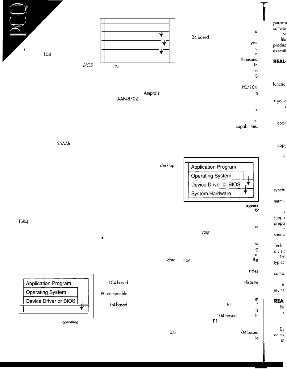
code into an EPROM,
after assembling or com-
piling it into separate code
and data address spaces. If the
application is relatively simple, you
may feel inclined to do the same thing
with your PC/
project.
It so happens that the PC architecture
has a handy mechanism called a
extension that lets you execute code within
an EPROM on system startup. The exten-
sion is a standard feature of the PC BIOS.
In fact, your PC’s video BIOS software is
loaded from a BIOS extension EPROM
located on your VGA display controller
card. Here’s how it works.
After system initialization and self test,
but before booting the operating system
from a floppy or hard drive, the BIOS scans
upper system memory on 2-KB boundaries,
looking for specially formatted blocks of
code to execute. These blocks must start
with the data pattern
If this pattern is found, the BIOS reads a
length byte and performs a checksum on
the remainder of the block. If the checksum
is correct (it must equal 0), the BIOS per-
forms a
FAR CALL
to the fourth byte of the
BIOS extension. In this manner, you can
run a simple embedded-PC application out
of an appropriately formatted EPROM.
However, you may want to think about
the limitations of this approach before
using it. Specifically, since BIOS exten-
sions run before DOS boots, you can’t take
advantage of DOS services or DOS-loaded
device drivers (or
You can, how-
ever, use
B I O S
s e r v i c e s .
Also, don’t count on using your favorite
compiler since many compilers require a
DOS run-time environment to execute their
compiled code. Listing 1 provides an ex-
ample of a BIOS extension that simply
outputs a message to the screen and returns
control to the BIOS.
Svstem Hardware
Figure 3: By
bypassing the
system,
BIOS,
and
device drivers, the user gets to
direct/y control system hardware, but loses
the advantages of an object-oriented
approach.
64
Application Program
I
Operating System
Device Driver or BIOS
System Hardware
Figure A well-behaved software is
characterized by a layered software
architecture.
For more information on how to create
a BIOS extension, check
applica-
tion note
DOS-BASED APPLICATIONS
If you’re like most embedded-PC de-
signers, you probably write your applica-
tion in C, compile it into an EXE file, and
run it under DOS. Plain old DOS.
But, why use DOS?
Even if your application has no need for
any operating system services whatsoever,
DOS may offer some important benefits:
l
DOS lets you use your favorite
PC compiler and debug tools by provid-
ing the required run-time environment.
As a result, you can program an embed-
ded application without any special
embedded tricks (or compilers)!
l
With DOS in your embedded system, the
target and development environments
are exactly the same. This parallelism
simplifies the task of porting your appli-
cation from the development computer
to the embedded target computer. Life
becomes easier in a lot of ways.
Even if your embedded application
doesn’t require DOS service, DOS or
DOS-based utilities ease system instal-
lation and maintenance. For example,
an MS-DOS Interlink utility transfers
to and from the system.
On the other hand, it’s not unusual for a
For example, imagine an intelligent
PC/
embedded application to
log data on or read parameter files from a
PC/l
paint-mixing machine that
floppy.
reads color matching parameters from a
floppy. It could easily be programmed to
support an endless variety of paint brands
or customerdefined requirements.
Another example might be a PC/l
basedenvironmental monitoring instrument
CIRCUIT CELLAR INK APRIL 1996
which logs its data onto a hard drive fo
subsequent analysis.
r
Where do you get DOS licenses for
PC/l
embedded system?
It depends on what kind of DOS
need and how many copies you require
For real MS-DOS, buy a few copies fror
the local computer store or a few
from Microsoft. For needs somewhere
between, try Annabooks. They’ve bee
designated by Microsoft as an MS-DO:
distributor for the PC/l 04 market.
There are also a couple of
oriented DOS alternatives. Datalight offer
ROM-DOS and General Software ha
IS
Embedded DOS. These products offer som
e
interesting enhancements peculiar to en
bedded-system requirements. Embedded
DOS includes normal DOS functions
IS
well as real-time, multitasking
GET REAL!
“But, real-world applications can’t ru
on a PC,” you say?
n
Figure 2: Some application programs
the operating system, communicating direct
with the drivers or even the hardware.
What? Are you worried that DOS is to
“soft” for
rugged, perhaps missio
critical application? What should you dc
For sure, there are many embedde
applications that must continue runnin
around the clock without operator interve
Perhaps, your embedded PC is
heart of an automated toll booth.
No doubt, you’ve seen this message c
your desktop PC: “Press to continue..
What happens when DOS outputs th
message to a PC/
system wit
What if it stops running? Everyone
free until the technician arrives to reboot
out a screen or key? Someone has
This is nice for the commuter, but a
for the Transit Authority. And for you,
press reset, that’s what!
might mean you lose the next contract!
Don’tdespair! Turning a PC/l
system into a real-time machine is the so
n-
)?
it!
it
to
wide
I
A m
time su
througt
benefit
ties
ecuti
l
funct
it’s ti
or fu
l
you
l
initic
be
On
vided
basic
switch
order
netwo
In
work
brarie
the lit
DOS
you
time
more
real-ti
use
purpose of a sizable group of real-time
software companies. And, the result is a
wide variety of excellent alternatives.
like to divide these real-time software
products into three categories: libraries,
executives, and operating systems.
REAL-TIME LIBRARIES
A minimalist approach to adding real-
time support to a PC/l 04 application is
through the use of a real-time, multitasking
function library. There are several potential
benefits to this approach:
l
you don’t need to deal with the complexi-
ties of a more full-featured real-time ex-
ecutive or operating system
l
function libraries often include full source
code, which may prove invaluablewhen
it’s time to debug or tune the application
or functions included in the library
l
you usually aren’t required to pay
copy royalties
l
initial out-of-pocket expenses are likely to
be low
On the other hand, the functions pro-
vided by the library are usually limited to
basic things like task management, task
switching, queue management, and event
synchronization. You won’t get
order services such as memory manage
ment, console I/O, serial communications,
networking, or a file system.
In short, if you need basic multitasking
support for a real-time application and are
prepared to
do
the hardware management
work yourself, this approach may be rea-
sonable. Two typical real-time function li-
braries are Interwork from Block Island
Technologies and DIVVY from the Drumlin
division of Micro/sys.
Table
1
shows what is offered by a
typical real-time library. As you can see,
the library’s functions are quite primitive in
comparison to what you’d expect from
DOS or Windows! listing 2 shows how
you might use these services to manage a
multitasking application.
REAL-TIME EXECUTIVES
Next in order of complexity are the real-
time executives. These packages provide
more system services than the multitasking
real-time libraries.
Despite additional vigor, real-time
mean.“They
use system resources-hardware and
PC-Based Instruments
HUGE BUFFER
FAST SAMPLING
SCOPE AND LOGIC ANALYZER
C LIBRARY W/SOURCE AVAILABLE
POWERFUL FRONT PANEL SOFTWARE
DSO Channels
2
Ch. up to 100
1 Ch. at
4K or 64K
Cross Trigger with
L A
125 MHz Bandwidth
Logic Analyzer Channels
$1799 DSO-28204 (4K)
$2285 DSO-28264 (64K)
8 Ch. up
to 100 MHz
4K or 64K
Cross Trigger with DSO
PAL
GAL
EPROM
EEPROM
FLASH
MICRO
Free
software updates on BBS
Powerful menu driven software
up to 128 Channels
up to 400 MHz
up to 16K Samples/Channel
Variable Threshold Levels
8 External Clocks
16 Level Triggering
Pattern Generator Option
$799 LA121 00 (100 MHz, 24 Ch)
$1299 LA32200 (200 MHz, 32 Ch)
$1899 LA32400 (400 MHz, 32 Ch)
$2750 LA64400 (400 MHz, 64 Ch)
Call (201) 808-8990
Link Instruments
369
Passaic Ave, Suite
100, Fairfield, NJ 07004
fax:
808-8786
1996
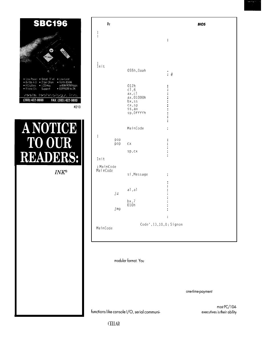
Circuit Cellar
will
occasionally provide a
listing of subscribers to
vendors with offers of
substantial interest to
our readers. If you would
prefer not to be part of
this listing, send the
mailing label from the
front cover of Circuit
Cellar INK
along with
your request to:
Circuit Cellar INK
Subscriber Service
Department
P.O. Box 698
Holmes, PA 19043-9613
listing
Here’s an assembly language program structured as a
extension.
This initialization code is for a tiny model with code,
data, and stack in the same segment.
BIOS-END equ
00060h
end of RAM used by BIOS
DGROUP
GROUP PROG
PROG
SEGMENT BYTE PUBLIC 'PROG'
ASSUME CS:PROG, DS:PROG
Unitialize run-time code. place stack in RAM, all else in ROM
PROC FAR
db
ID pattern
Blocks db 1
of 512 blocks code and data
Entry
int
Get number of Kbytes in AX
mov
Divide by 64
shl
to get paragraph address
sub
64 Kbytes for stack
mov
Get caller's FAR return
mov
address
mov
Now set up
mov
the real stack
push cx
Save the caller's return
push bx
address on my stack
call
execute your program
if program exits (via a FAR return). control returns to the BIOS
bx
Get the BIOS
stack back
mov
ss,bx
Restore
mov
them
ret
and ret to BIOS and boot
ENDP
is a simple sample program. It signs on and returns.
PROC
NEAR
lea
Point to the message
MainCodeLoop:
cld
Ensure forward direction
lodsb
Get the next character
or
Is it the end?
MainCodeExit
Yes, exit
mov
ah,14
No, get TTY output parm
mov
Screen attribute
int
Output the character
SHORT MainCodeLoop
and loop for more
MainCodeExit:
ret
Return to BIOS
Message db
'Main
message
ENDP
PROG
ENDS
END
ware--thriftily, and are performance-ori-
ented. Also, most real-time executives are
offered in a
only use
(and payfor)thecomponentsyou need.
Depending onyourreal-timeexecutive,
you can get just about any function you
need. The core component, called a ker-
nel, provides basic system and task man-
agement and control including resource
initialization,
task
queuing and switching,
memory management,and so forth.
Optionalsoftwarecomponentssupport
cations, networking, disk read/write, and
so on. Figure 4 illustrates the key services
offered by a typical real-time executive.
Depending on the vendor, source for
both the kerneland device drivers may be
available, so you can troubleshoot sticky
problems yourself. Also, real-time execu-
tives are commonly (though not always)
sold on a
basis, which
eliminatesthecostandoverheadofpaying
royalties each time you build a system.
An interesting feature of
oriented real-time
6 6
CIRCUIT
INK APRIL 1996
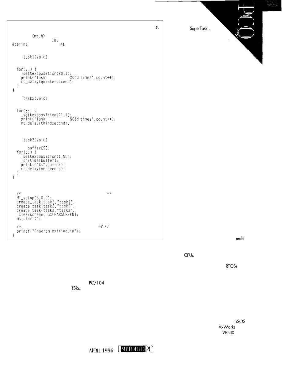
listing 2: A sample C application uses the DIVVY real-time functions presented in Table
#include
#define onesecond
quartersecond
#define thirdsecond 6L
void
static unsigned int count:
1 has run
void
static unsigned int count:
2 has run
void
char
main0
3 tasks, no flags, standard tick rate
5, 2048, NULL);
5, 2048, NULL):
5, 2048, NULL);
system is multitasking here until
Kodak’s AMX, U.S.
Software’s
and
Microtec Research’s VRTX are
good examples of real-time ex-
ecutives.
REAL-TIME OPERATING SYSTEMS
to be used alongside DOS. Your system
boots from DOS and then loads the execu-
tive and your application from an EXE file.
Real-time executives with this capability
usually provide a function call so your
application can use DOS and BIOS ser-
vices such as file or console I/O. You can
therefore use DOS device drivers
and
Assume that the appropriate DOS net-
work drivers are present to convert the
network drive into a local DOS resource.
Your application-running under a real-
time executive-can then access a remote
disk drive across an Ethernet LAN using
DOS file read/write services.
Keep in mind that DOS and BIOS are
not reentrant, so only a single task can be
permitted to access BIOS or DOS functions
at a time. To prevent problems, the real-
time executive must provide a suitable
“locking” mechanism.
Although this restriction may be unac-
ceptable in some systems, quite a few
applications don’t need shared
access to peripheral resources such as a
disk, display, network, or keyboard. They
therefore benefit from this approach.
Another problem exists if your applica-
tion needs to run in protected mode. To
take advantage of BIOS or DOS services,
a protected-mode application needs to
switch in and out of real mode, which
would result in unacceptable inefficien-
cies.
At the high end of the scale is the full-
featured real-timeoperating system (RTOS).
“What’s the difference between a real-
time executive and a real-time OS?” Since
there’s no universally accepted answer to
this question, I’ll give you my version.
An executive manages the computer’s
basic resources-CPU, memory, interrupts,
timers, and DMA. An operating system
does all this while managing the system’s
peripheral devices, which typically include
disk drives, keyboard and display, serial
communications, and networking.
In truth, a lot of RTOS offerings are
modular, consisting of a real-time kernel
and an assortment of device managers. As
a result, it may be difficult to decide whether
a particular package is a real-time execu-
tive or a real-time OS.
In a minimal configuration, it may fit the
definition of an executive. Yet, when its
peripheral device managers are included,
it becomes a full-fledged RTOS.
In fact, it doesn’t matter what you call it!
It’s a full-fledged RTOS if:
l
it includes all the basic services of a real-
time executive (described earlier)
l
it includes file system, console I/O, com-
munications, and networking
l
once running, it completely eliminates
the use of the normal PC BIOS
l
all these functions support full,
threaded (multitasking) operation
l
it can do all this in protected mode (on
‘386
and up)
Increasingly, PC-compatible
pro-
vide GUI support with built-in drivers for
VGA display, a standard PC keyboard,
and a standard mouse. took at Figure 5 to
get an idea of what you can easily accom-
plish using this kind of RTOS GUI.
Some popular PC/l 04-oriented prod-
ucts appearing to meet all of these require-
ments are QNX from QNX Software
Systems, Lynx from Lynx Real Time Sys-
tems, OS-9000 from Microware,
from Integrated Systems,
from
Wind River Systems, and
from
Venturcom.
67
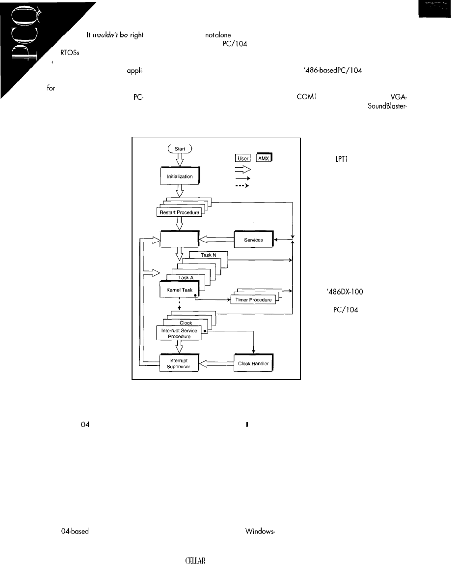
to leave the subject of
without talking about
device drivers.
Assuming your RTOS and
cation runs in protected mode, device
drivers
all hardware must be 32-bit,
reentrant code. The RTOS can’t use the
compatible BIOS since the BIOS doesn’t
meet this condition. So, the RTOS you use
must replace the BIOS with its own version
of the functions within the BIOS.
This is a blessing and a curse.
You can expect improved speed
and robustness. However, any non-
standard hardwarefunctionsin your
PC/l O&based system require pro-
tected-mode drivers for your par-
ticular RTOS and hardware.
An RTOS claiming to support
PC/l 04 applications should pro-
vide a complete set of drivers for all
standard PC-compatible controllers
and peripherals. What you need to
worry about is support for embed-
ded-PC extensions such as watch-
dog timers and solid-state disks or
interfaces like PCMCIA, SCSI, and
LAN adapters since these haven’t
attained chip-level standardization
with desktop PCs.
Don’t be surprised to find your-
self haggling with both your RTOS
and hardware suppliers over who
should supply the drivers! You may
end up creating some yourself.
In some cases, you can circum-
vent the RTOS driver problem by
using a real-time executive, instead
of an RTOS, along with DOS. How-
ever, this
only
works in applications
that don’t run in protected mode or
need multithreaded access to the
resources in question.
You’recertainly
in this thought.
There are quite a few
applica-
tions, both completed and under develop-
ment, that use Windows!
But, you may object that you can’t
implement a real-time system using Win-
dows.
However, this depends on your defini-
tion of “real time.” Or, to be more practi-
cal, it depends on your real-world
application’s performance requirements.
Control Flow
Function Calls
Interrupts
Task Scheduler
But if your application demands quick
response to external stimuli, efficient use of
A
CPU module
system resources, or high confidence in
runs Windows 95. A touchscreen emulates
a standard serial mouse and is connected
uninterrupted system operation, you’d be
to
while the display is a
compatible color LCD. A
better off with a full-fledged RTOS.
compatible PC/l 04 module adds speech
and musical audio output, and the data-
base is stored on a hard drive. A
CD-ROM provides animation and
entertainment, and a small thermal
printeron
generates hardcopy
of selected information and sale
coupons. The database is periodi-
cally updated from a central office
over a modem connected to COM2.
You could easily run this entire
application within Windows or
Windows 95. If you found the sys-
tem too slow at accessing the hard
disk, reading the CD-ROM, or up-
dating the display, you’d
simply do
what you would with your desktop
PC-upgrade the CPU!
For this application, a ‘386SX
or ‘486SLC is probably too slow,
but a
would be fine.
Fortunately, these are now avail-
able in
modules. Next
year, you’ll be able to upgrade to
a Pentium-based PC/l 04 module!
My point-if millisecond re-
sponse times aren’t needed, you
may be pleasantly surprised with
the capabilities of the world’s most
popular multitasking operating sys-
tem (yes, that’s Windows!). Don’t
forget to provide an externally ac-
cessible reset button or a watch-
dog-timer.
Figure 4: The functions offered by AMX are representative of
typical realtime executives.
Officially, a real-time system is one that
behaves deterministically. But, prefer to
think of it as any system that needs to
With my definition, a real-time system
provide enough performance to success-
interact with external real-world stimuli
fully perform its defined task. Some appli-
cations require millisecond precision while
during its operation.
others respond to a single event per hour.
Under this interpretation, even Win-
dows can support some real-time require-
ments! (Please don’t be offended, anyone!)
What’s an example of a
based PC/l 04 embedded system?
While many
PC/I
applications meet
these constraints, others do not. Beware!
DO YOU DO WINDOWS?
Despite all this talk about the exotic
world of real-time libraries, executives,
and operating systems, you may be won-
dering about Windows. It has the ability to
manage system memory and protected
mode, run multiple tasks, support graphics
functions, and simplify user interfaces.
So, why not use Windows (or Windows
95) in a PC/l
embedded appli-
cation?
Consider an information kiosk at an
airport. It offers information about shop-
ping, local entertainment, and community
services.
DON’T FORGET THE BIOS
With all this discussion of application
and operating system software, don’t over-
look a very intimate part of every PC/l 04
system: the CPU module’s BIOS. After all,
it’s responsible for some important stuff:
l
initializing the CPU, memory, and sys-
tem/peripheral controllers
68
CIRCUIT
INK APRIL 1996
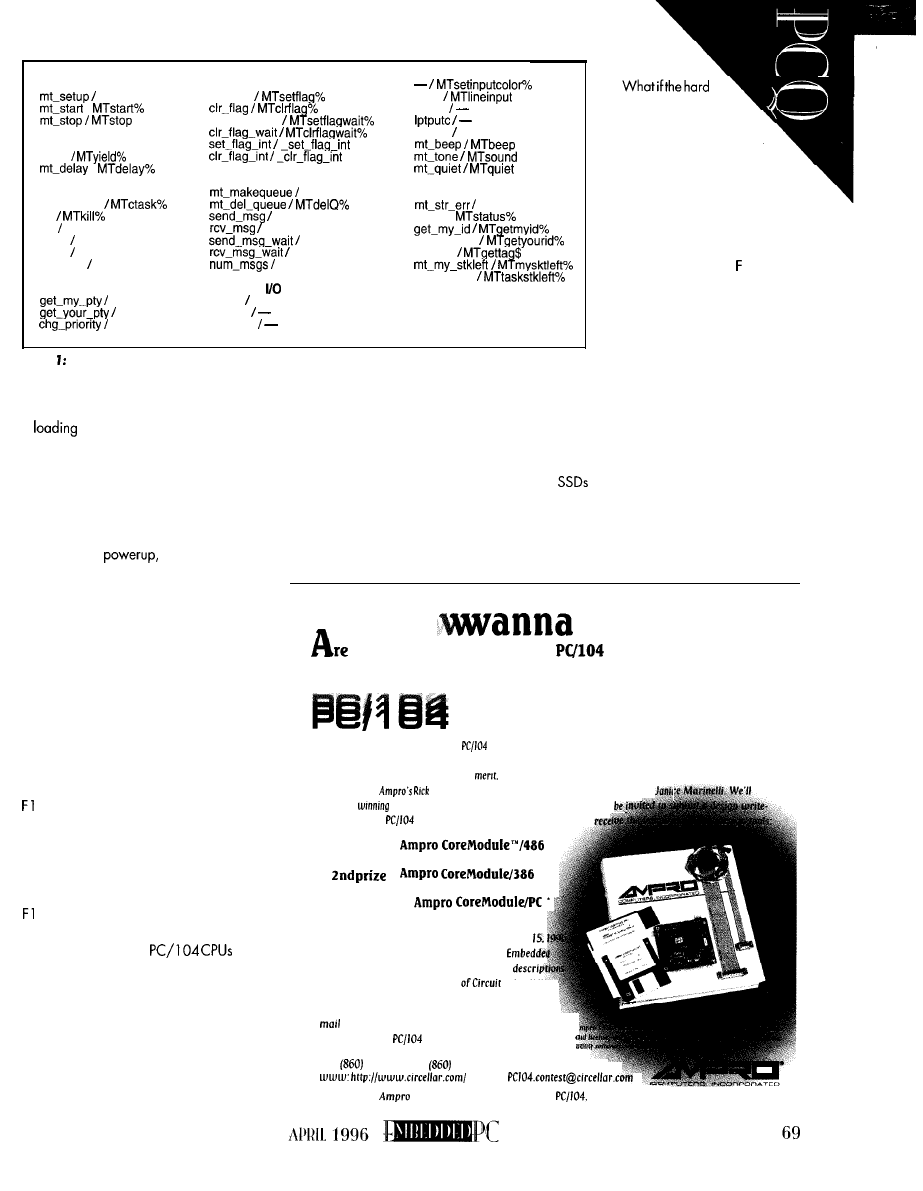
Startup and Exit
MTsetup%
I
Dispatcher and Timing
yield
I
Task Control
create-task
kill
die MTdie%
sleep MTsleep%
wake MTwake%
suspend MTsuspend%
Priority and Tags
MTgetmypri%
MTgetyourpri%
MTchgpri%
Flags
set-flag
set-flag-wait
(assy)
(assy)
Queues
MTmakeQ%
MTsendmsg%
MTrcvmsg%
MTsendmsgwait%
MTrcvmsgwait%
MTnummsgs%
Standard
tgetch MTinkeywait$
tgetche
tungetch
tgets
tcgets
lptputs MTlprint%
Status
MTerrorstr$
status I
get-your-id
get-tag
task_stkleft
Table The functions offered by a typical real-time library don’t compare with what you can get in
DOS or Windows, but can get a lot of simple jobs done.
l
performing the system power-on-self-test
l
BIOS extensions (if present)
l
booting the operoting system (if present)
l
providing hardware interface support
during system operation for keyboard,
disk, serial, parallel, and timer functions
These ore important things to get right!
What if, on
a system perform-
ing critical control or monitoring functions
doesn’t successfully boot its operating soft-
ware? What if that system offers security
surveillance or temperature or pressure
monitoring? System failure could endan-
ger lives or property. In an intelligent vend-
ing machine, down time costs its owners
substantial revenue.
What if a hard
disk drive spins up a bit
too slowly after a power brownout? When
the BIOS fails to boot the operating system
from a not-quite-ready disk drive, a normal
desktop PC hangs until someone presses
or reset. Such a failure mode is undesir-
able-more likely, unacceptable-in many
(most?) embedded applications.
Your PC/l 04-based application may
need to perform its task around the clock
without failure. With its reliance on “Press
to Continue,” the normal desktop-PC
BIOS doesn’t make it easy for you to sleep!
Fortunately, some
now
include BIOS enhancements that address
the special concerns of embedded applica-
tions. Here are some features you should
look for in an embedded-PC BIOS:
l
Battery-free startup
Did you know your desktop PC won’t
power up and boot when the battery that
l
Fail-safe boot
drive spins up slowly
or there is a soft read
error when
the BIOS attempts
to boot?
An embedded-PC BIOS accom-
modates this condition by looping
(indefinitely) in its attempt to boot
from the designated boot device. It
won’t just give up and display,
“Disk Read Error, Press 1 to Con-
tinue...”
l
Solid-state disk support
Conventional disk drives may
simply be too “soft” for reliable
operation in your PC/l 04-based
embedded application. Your con-
backs up the CMOS setup data (in the real-
time clock chip) is dead?
Eliminate this risk by keeping a redun-
dant copy of the setup data in a tiny
inexpensive EEPROM. In fact, you can
eliminate the battery entirely (an actual
requirement for certain applications), pro-
vided you don’t need a battery-backed
time-of-day clock function.
cerns may include shock and vibration,
operating temperature, mechanical fail-
ure, and speed.
You may need a solid-state disk (SSD).
can be nonvolatile RAM (NVRAM),
EPROM, or flash memory. Whatever SSD
you choose, the BIOS probably needs to
support it.
be famous?
you or your company using
technology in an
interesting or unusual way? Tell us about it.
DESIGN CONTEST
CO
You are invited to submit unique
projects or applications to our design contest. Be sure to include
functional block diagrams with descriptions of the hardware. software. and peripherals used. Contest
entries will be judged for technical
applicability. and originality. The judges: Circuit Cellar
INK’s
Steve
Ciarcia.
Lehrbaum. and Embedded PC’s Managing Editor
highlight
applications in Embedded PC. plus designers
will
up for a future
Quarter. And there’s more! Winners will
l
1st prize
Development Kit
l
Development Kit
. 3rd prize
Development Kit
All entries must be received no later than August
Winners will be announced at September’s
Systems Conference and the winning project
will appear in December’s issue
Cellar INK,
Contact us today for your entry form and then
your contest entry to:
A
Janice Marinelli.
Quarter Contest
Circuit Cellar INK 4 Park Street Vernon, CT06066
Tel:
8752199 Fax:
872-2204
E-mail:
‘sponsored by
Computers, Inc., the originator of
and Circuit Cellar INK. home of Embedded PC
Has your desktop PC
ever crashed? (Dumb ques-
tion, right?) You reach for the
power switch or reset button. No
great harm is done. You lose ten min-
utes of editing that you can usually
On the other hand, if your embedded
PC crashes, no one may know anything is
wrong-let alone be able to restart it.
These occasions mark the times a simple
embedded-PC enhancementsaves the day.
It’s inexpensive and easy to include a
watchdog timer on a PC/l 04 CPU. But, for
best results, the embedded-PC BIOS needs
to support the watchdog timer function.
l
Fast boot
Some embedded systems can’t tolerate
the lengthy self-test and startup delays typi-
cal of a desktop PC. The system may need
to be up and running within a few seconds,
not tens of seconds. Your embedded-PC
BIOS should let you shorten initialization.
l
Serial console
Your PC/l 04-based embedded system
may not include normal desktop-PC
interface hardware like a PC keyboard,
VGA controller, or CRT monitor. Yet, there
may be times when you need to see what’s
going on
DOS (or application) prompt.
Your BIOS should offer you the option of
routing the DOS console (keyboard and
display) functions to a serial port.
l
Serial loader
Another useful enhancementcomesfrom
a BIOS function that loads executable code
through a serial port prior to system boot.
This feature can load a test program or
reformat an internal disk drive (or SSD) that
lost data or requires an update.
l
System customization hooks
Your embedded system probably in-
cludes specialized hardware for keypad
input, data display, or real-time control.
Often, such devices need to be initialized
immediately on
(i.e., before the
system loads the OS and application).
You might think you need BIOS source
code to customize the BIOS. But, once you
find out how much it costs, you’ll change
your mind. (You’d rather buy a BMW!)
Fortunately, some
in-
clude a BIOS enhancement that lets you
70
Figure 5: A typical user interface implemented using services provided by photon, the QNX
includes elements familiar most GUI users.
patch in custom initialization routines. You
don’t need to buy and modify BIOS source.
NOW, FOR MY FAVORITE APP
A couple of years ago, following one of
my
seminars, a member of the
audience described what has become my
all-time favorite embedded PC/l 04 soft-
ware story.
His project for UC Santa Barbara was a
PC/l 04-based atmospheric datacollection
system carried aloft by a weather balloon.
The data was collected and transmitted by
two-way radio to a ground station. He also
used the two-way radio to modify the
application program from theground while
the balloon was aloft.
Initially, he ran into a problem. The
radio transmission data rate was too slow
to upload (literally!) the entire application
program. So instead, he used an embed-
ded PC/l 04 CPU’s special features.
He put the application source code,
DOS editor, and C compiler directlyon the
system’s disk drive. He enabled the serial
console option of the PC/l 04 CPU, which
routed the DOS console (keyboard and
display) functions through the radio mo-
dem (via the
serial port).
This way, when he modified the appli-
cation, he could perform the same steps as
on a desktop PC: exit the program, start the
editor, edit the source code, compile the
application, and run the recompiled code.
INK
1996
I call this “Compiling on the Fly.” Some
programmers sure do have guts. I’d defi-
nitely recommend the CPU’s watchdog
timer function in a system like this!
Think what happens if the recompiled
program crashes! Do you think he tested
the code on the ground first before perform-
ing the edit, compile, and execute process
in the air? bet he did!
YOUR FAVORITE APP?
I’d like to find out what your favorite
application is. Check the advertisement on
page 69. No doubt, you’ve come up with
a splendid PC/l 04 application that we all
need to hear about. Write it up and send it
in. Not only might you win one of three
prizes, but you just may end up being one
of PC/l 04 Quarter’s greats.
So, what is it? Do
wanna be fa-
mous?
Special thanks to Drumlin for Table and
to Kadak Products and QNX for the Figures
4 and respectively. Your support is
greatly appreciated.
Rick
Comput-
ers where he served as vice president of
engineering from
to
Now, in
addition to his duties as
president,
Rick chairs the
Consortium.
CONTACTS
Application Note
Computers, Inc.
990
Ave.
Sunnyvale, CA 94086
(408) 522-2 100
Fax: (408) 720-l 305
3447 Ocean View Blvd.
Glendale, CA 91208
(818) 244.4600
Fax: (8 18) 244-4246
Embedded MS-DOS
Annabooks
1 1838
Plaza Ct.,
102
San Diego, CA 92 128.24 14
(6 19) 673.0870
Fax: (619) 673-l 432
Real-Time Executives
AMX
Kadak Products, ltd.
206-l 847 West Broadway Ave.
Vancouver, BC
Canada
lY5
(604) 734.2796
Fax: (604)
1 14
DOS
Alternatives
ROM-DOS
Dotalight
307 N. Olympic Ave., Ste. 201
Arlington, WA 98223
(360) 4358086
Fax: (360) 4350253
U S Software
142 15 NW Science Park Dr.
Portland, OR 97229
(503) 64 l-8446
Fox: (503) 644.2413
Embedded DOS
General Software, Inc.
320 108th Ave. NE, Ste. 400
WA 98004
(206)
Fax: (206) 454.5744
VRTX
Microtec Research
2350 Mission College Blvd
Santa Clara, CA 95054
(408) 980-l 300
Fax: (408) 982.8266
Real-Time Function libraries
Block island Technologies
15455 NW Greenbrier Pkwy., Ste. 2 10
Beaverton, OR 97006
(503)
1
Fax: (503) 6457732
Real-Time Operating Systems
QNX
QNX Software Systems, ltd.
175 Terrence Mathews
ON
Canada
1
(613)
Fax: (613) 591.3579
DIVVY
Drumlin Division
Lynx Real Time Systems
Here’s a great deal on new
12 volt 9 amp/hour
rechargeable lead acid bat-
teries. These batteries
were recently manufactured
and prepped for use in a
product which hasn’t yet
to market. The OEM didn’t
to hold them in stock, so we got
them at a greatly reduced price. They are 5.9”
2.55” x 4.42” high and have a strip of foam
padding stuck to one side.
They have standard
quick-connect/ solder terminals.
Wt: 8 Ibs.
GC-129
NSL 4582
Sulfide photoconductive cell.
ohms in bright light. 2 meq ohms dark.
I
16780 Lark Ave.
Los Gotos, CA 95030
(408) 354-7770
Fax: (408) 354-7085
OS-9000
Microware
1900 NW 114 St.
Des Moines, IA 50325
(515)
Fax: 15) 224-l 352
p s o s
Integrated Systems Inc.
3260 Jay St.
Santa Clara, CA 95054
(408) 980-l 500
Fax: (408) 980.0400
Wind River Systems
1010 Atlantic Ave.
Alameda, CA 94501
(5 10) 748-4 100
Fax: (510) 814.2010
Inc.
2 15 First St.
Cambridge, MA 02 142
(617)
Fax: (617) 577-l 607
422
Very Useful
Moderately Useful
424 Not Useful
Visit Our World Wide Web Site...
CHERRY
S.P.D.T.
Body size: 0.51” long X 0.255” high
X 0.255” wide. Lever with ridged end
simulates roller action. Rated 3
amps 125
2 amps 30 Vdc.
Miniature silicon solar cell converts liaht
impulses directly into electrical charges which
can easily be amplified, using a transistor
for example, to activate a control mechanism.
Unlike a conventional photo diode or transistor,
it generates its own power and does not
require any external bias. Generates 0.4 vdc
in moderate light. Silicon cell is mounted on a
0.31” 0.23” 0.07” thick plastic carrier and
has pc leads on 0.2” centers.
Large quantity available.
CAT # PVD-2
Optex
Invisible infrared beam and
switch is useful for a vari-
ety of security, safety and
sensing applications such
as perimeter alarms, elec-
tric gate or garage door
controls or conveyor line
sensing. Modulated beam covers a 20 meter dis-
tance even with poor
IP-66 enclosure
makes it dust proof and splash resistant, suitable fo
most outdoor conditions. Light/dark switching selec-
tor. Sensitivity adjustment control. LED power and
sense indicators. Two position cable entry gland
deg. apart) accepts
threaded conduit and a
ety of wire sizes. Glass fiber-reinforced plastic
ings are 3.05” 2.5” 1”. Supply voltage:
Solid State Output: 0.5 amp (must have load tc
operate). Includes mountina brackets and hardware
and
listed.
CAT # PES4
ALL ELECTRON
k
ac aging
Far too often, packaging is
to the end of the design phase. However, it can
make the
between a design being a kludge and a reliable product.
Russ categorizes design types, suggesting which type is best to use when.
the past few columns, I’ve looked at the
attributeswhich makeembedded
lar, investigated the various buses and
boards available, and explored some of
the intricacies of driving clusters of small
displays in embedded applications.
It’s time now to take a look at the various
options available for physically packaging
embedded systems.
Generally, the end use dictates how an
embedded system must be packaged. The
options fall into four main categories:
l
open-frame construction
l
rack-mount systems
l
PC embedded within the display
l
portable and hand-held units
I’ll look at each of these approaches in
detail, checking out the specific hardware
components available to the system de-
signer in each category. Since
packaging was covered in
04 Quar-
ter” (INK
I’ll avoid PC/l
systems here.
72
Packaging often takes a back seat to the
more glamorous aspects of implementing
an embedded system, such as system de-
sign, CPU and interface selection, and
programming.
Yet, packaging is critical to the imple-
mentation of a robust and efficient design.
It requires that you take into account the
overall degree of integration, shock and
vibration, cooling, and powering aspects.
Packaging can make the difference
between creating an unreliable kludge that
never seems to get completed or work right
and a reliable, serviceable product.
O P E N - F R A M E C O N S T R U C T I O N
Anyone following Circuit Cellar’s HCS
applications is familiar
with
propensity for screwing modules and sys-
tem components to large wooden boards
and hanging them on the wall.
This structure represents the extreme in
“open-frame” construction! Few embed-
ded system applications lend themselves to
such a state of “open” construction.
INK
Nevertheless, the benefits of this ap-
proach are many:
l
rapid and flexible configuration
l
ease of servicing
l
simple modification and modular expan-
sion
l
adaptability to various form factors
l
robustness and good cooling in benign
environments
When using this approach, you just need
to select the system components and then
conveniently arrange,
fasten, and intercon-
nect them. With modifications, this ap-
proach can be used in other applications.
I’ve mentioned before an ATM de-
signed for bank lobbies. In this case, the
system components were certainly not
bolted to a piece of wood hanging on a
wall. But, the
components (CRT dis-
play, keypad, ticket printer, deposit enve-
lope chute, gating solenoid, and collection
bin) were fastened to various custom brack-
ets fastened to the enclosure.
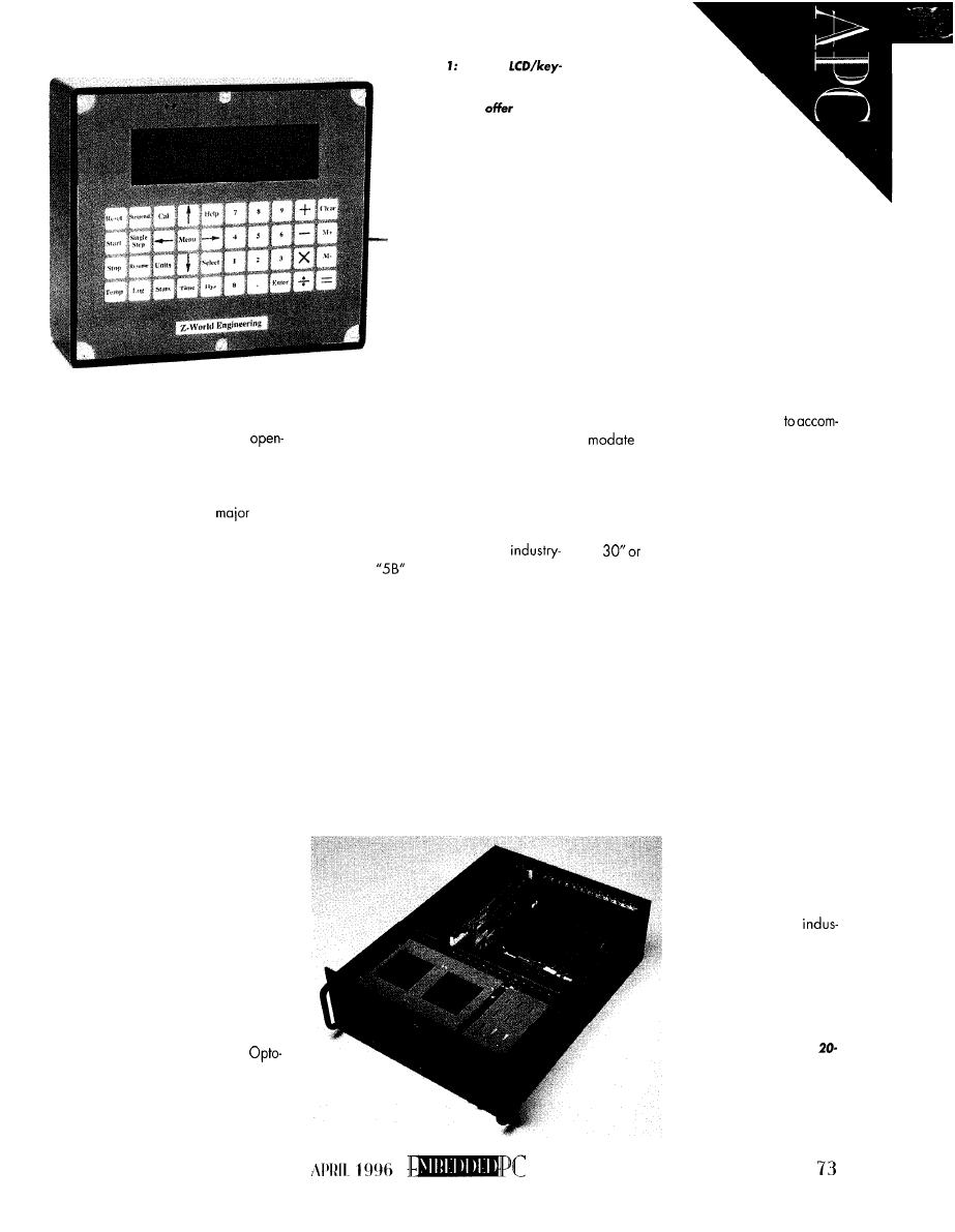
The rest of the electronics-a floppy
disk drive for booting the program and
saving transaction data-were bolted
frame fashion to a large metal shelf within
the ATM housing. A wiring harness with
numerous disconnect points provided elec-
trical interconnect between the
com-
ponents and the electronics shelf.
In this manner, any element of the sys-
tem could be easily removed for replace-
ment or servicing. While the approach
may seem unorthodox, it was perhaps one
of the most cost-effective, yet serviceable,
systems I’ve ever seen.
When using this open-frame approach,
you need to give careful consideration to
mounting stiffness. Warping, twisting, flex-
ing, or bending of electronic components
can wreak havoc with circuit-board reli-
ability and lead to early failure.
Often, getting the right rigidity requires
design and fabrication of custom brackets
to handleeach subassembly. While thicker
plywood works for prototypes and home
use, sheet-metal panels are normally used.
They
should be reinforced with cross-braces
to resist warping.
When a number of circuit boards are
needed to implement the embedded PC
element of the design, a rack of STD, VME,
or MicroPC boards can serve as one of the
subsystems mounted totheelectronics shelf.
In many systems, interconnection with
real-world AC and DC signals is required.
When discrete digital I/O is involved,
connection can be achieved through
22 assemblies (named after their origina-
tor, but available from many other sources).
These racks, which are most likely famil-
iar to many of you, house a wide variety of
photo Modular
boardpackayer like the one
pictured here from Z-World
Engineering
a quick
and inexpensive operator
interface in some low-end
embedded PC applications.
Purchasing an off-the-shelf
unit can save valuable engi-
neering time and effort.
AC or DC input/output
modules for interfacing
logic levels to real-world
AC and DC voltages and
currents. The optoisolated
interfaces provide excel-
lent isolation from tran-
sients caused by starting motors and
inductive kickback from relays for the com-
puter and other low-voltage logic signals.
A similar panel supports signal-condi-
tioning equipment for real-world low-level
sensors such as thermocouples, optical
sensors, pressure transducers, and so on.
Similar in appearance to the Opto-22 car-
rier boards, these units accept
standard
analog and digital I/O
signal-conditioning modules.
The output of these modules then con-
nects to A/D and D/A converters within the
embedded PC. Modules are available for
connecting low-level thermocouples (com-
plete with cold junction compensation) and
a host of other data-acquisition functions.
For user interaction in embedded sys-
tems, a conventional CRT monitor and PC
keyboard are often unsuitable. However,
small modular keypad and display sub-
systems, like that shown in Photo 1, may be
adapted quickly to meet custom needs.
You mightalsoconsider
the small embedded dis-
plays I discussed last time
(INK 67).
R A C K - M O U N T S Y S T E M S
A N D C A R D C A G E S
The most classical housing for industrial
and laboratory embedded systems is the
conventional card cage which mounts in
relay racks. The cages are best suited to
situations where other large instruments
are needed to complete the overall system.
The components generally are bulky
and heavy, requiring a sturdy structure to
hold them all together. Relay racks have
been used for this purpose for as long as
there have been electronic instruments.
Relay racks come in a variety of sizes
and styles.
They
are usually sized
devices 19” wide, though some
handle 24” units. The racks range from 1’
to over 7’ in height and may be bolted into
bays for very large systems.
Stylish units are available which mount
under a desktop work surface. With depths
of
more, it is often possible to mount
equipment from both the front and rear,
which essentially doubles capacity.
When computers first arrived, it was
natural to mount them with the rest of the
system components. However, to accom-
modate the many circuit cards that make
up the computer and I/O electronics sub-
system, card cages are now used.
These cages are available for all com-
mon embedded PC bus standards: STD,
VME, ISA, MicroPC, and those typically
employing a passive backplane. The cages
usually include provision for mounting
power supplies, floppy and hard drives,
CD-ROMs, and other com-
puter peripherals.
A typical STD bus card
cage is featured in Photo 1
of my INK65 column. Op-
tionally, complete
Photo 2: Interlogic In-
dustries’ RK720 industrial
rack-mount computer sup-
ports ISA cards with a
slot passive backplane,
room for 3.5” drives, and
single or dual-redundant
power supplies running
from either
48 VDC or
110 VAC.
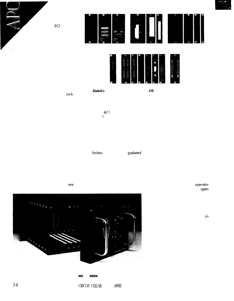
trial PCs, like shown in
Photo 2, use of conven-
tional ISA and
cards in
robust rack-mounted systems.
Getting signals in and out of the
card cage are big concerns. Two ap-
proaches are normally used. Connections
can be made to the backplane via transi-
tion connectors which terminate on custom
panels mounted to the rear of the relay
rack.
However, when it’s more convenient to
bring signals out the front of the rack, the
ancillary access plates [see Photo 3) pro-
vide a neat, clean, simple, and reliable
solution.
Powering the electronics in the card
cage is also important. Separate
mounted power supplies can be used when
the load is great, or you can use plug-in
supplies that fit into the card cage itself.
The reliability of the power supply has
become an important issue for embedded
systems. It seems that the power supply is
often the weak link keeping systems from
running reliably without interruption.
Ziatech recently introduced an STD32
card cage sporting dual power supplies
which keep the system running even if one
supply should fail. The backplane is de-
signed to hot swap, so the
faulty supply
can
be replaced without powering down the
system. This redundant power supply is
also available for Interlogic’s rack-mount
unit shown in Photo 2.
Embedded systems frequently operate
under extreme environmental conditions in
vehicles (trucks, tractors, aircraft, and
Photo 3:
removable and interchangeable
access plates provide a convenient and
robust means of bringing signals in and out of an embedded card cage PC.
tercraft) and industry. Kinetic Computer
has several rugged solutions.
Their NEMA
2 and MIL-STD-8 10,
-975, -1540, -46 -rated card cage (Model
RCC32 shown in Photo 4) tolerates up to
20-G shock and 12-G random vibration as
well as water spray, dust, and other con-
taminants. This ruggedness is achieved
through special backplane connectors, the
lock of the card and cage, special fins
which remove up to 100 W of
heat
from
the
sealed
enclosure, and
front panel for sealed MS connectors.
EMBEDDING PCs IN DISPLAYS
In embedded PC applications where
human interaction or data presentation is
paramount, the display is the most obvious
and important feature. With reduction in
Photo 4: For embedded PC applications in extreme environments involving water spray, high
shock, and vibration, Kinetic Computer’s RCC-32 rugged card cage provides a convenient
solution for STD-based systems while meeting
and
standards.
the size of computer electronics, you can
embed the entire PC within the display
subsystem itself. The number and variety of
such offerings are staggering.
If this approach suits your needs, you
should search carefully for the most highly
integrated solution possible. After all, there’s
not much sense in having all but 10% of
your system in one neat enclosure, when
you then have to go to extremes to find a
home for the remainder of the components.
There’s also little sense in attempting to
create a package yourself. Subtle consid-
erations like cabling, noise pickup, com-
patibility of flat-panel displays and touch
screens, and integration of operating sys-
tems and support software can quickly
destroy any savings.
At the low end, nearly every
control-panel vendor offers a simple,
frame display pack, like the one shown in
Photo 5. As you can see, it gets the display
portion of your design over with in a hurry.
Some of these units contain nothing but
a monochrome or color flat-panel display
and an optional touch panel. Others
cludeelectronicswhich interfaceateithera
digital or an analog level with a controller
in the PC assembly.
The analog flat-panel displays are par-
ticularly convenient as they directly replace
color VGA (and larger) monitors with no
hassle. But, these are often only partial
solutions that leave a lot of electrical and
mechanical design in your court.
More fully integrated solutions, like the
one shown in Photo 6, also include built-in
power supplies and provide numerous slots
for ISA cards and for mounting disk drives.
INK
1996
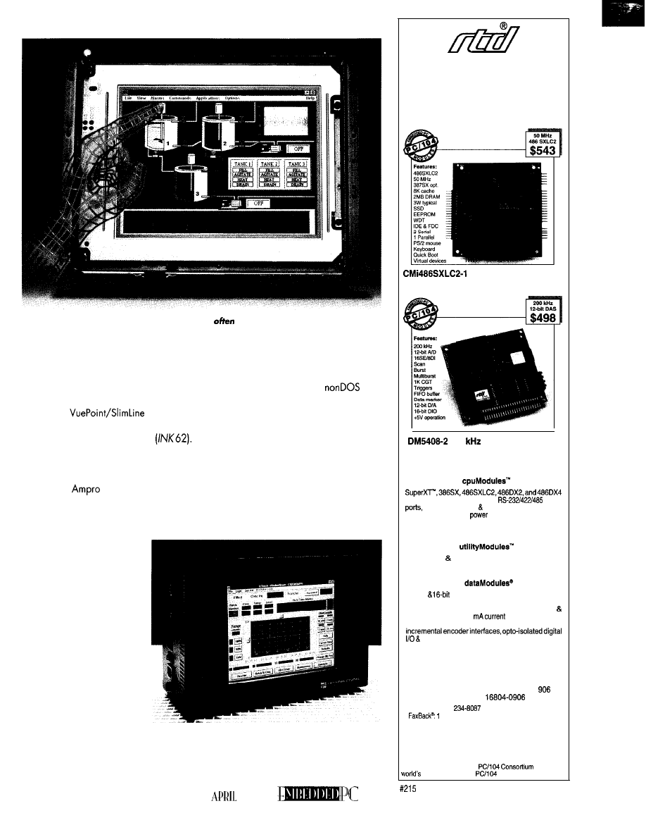
Photo 5: Simple OEM display requirements can
be met with modular packages like this
one from Teknor. Manufacturers
of similar units include Computer Dynamics and interactive
Display Systems.
A solution which combines the conve-
nience of an integrated operator control
panel with complete embedded PC, key-
board, and mouse, and is also rack mount-
able is the
offered by
Interactive Display Systems. It’s shown in
Photo 2 of my September column
There are also two other extremes in
embedded PC display systems. You can
have very small LCD subsystems like that
offered by
(see Photo 7). It can
marry neatly with a stack of PC/l 04 com-
puter modules.
At the other end are the
large,
bulky
CRT-based indus-
trial operator consoles which
have been around for years.
These cumbersome units have
given way to flat-panel tech-
nology. The consoles often
include touch screens and/or
sealed membrane keypads
and function buttons, which
survivewash down in extreme
environments.
HAND-HELD PCs
Only a few years ago, it
would not have been conceiv-
able to carry an embedded
PC in your attache case or
pocket. But now, there are
devices which permit just that.
Hand-held PCs are rapidly emerging
with almost unlimited applications. They’re
no longer limited to simple
solu-
tions built around 805 1 s in custom pack-
ages. You’re hardly ever forced to roll your
own or face high costs for portability.
While Two Technologies calls its offer-
ings hand-held terminals, in fact the com-
pany offers a complete line from dumb
terminals to complete hand-held PCs, like
the one shown in Photo 8.
At about $1000, these little computers
offer solutions to many portable computing
photo 6: Interactive Display Systems’ deluxe full-size enclo-
sure provides not only a flat-panel display (color or mono)
and optional touch panel, but also a complete embedded PC
and power supply.
Sets
the Pace
in Low Power,
High Performance
PC/l 04 Technologies
Fully Integrated PC-AT
with Virtual Device Support
200
Analog l/O Module
with Channel-Gain Table
Make your selection from:
9
processors. SSD, 6MB DRAM,
serial
parallel port, IDE floppy controllers, Quick
Boot, watchdogtimer,
management, anddigital
control. Virtual devices include keyboard, video,
floppy, and hard disk.
7
SVGA CRT LCD, Ethernet, keypad scanning,
PCMCIA, intelligent GPS, IDE hard disk, and floppy.
16
12, 14
data acquisition modules with high
speed sampling, channel-gain table (CGT), sample
buffer, versatile triggers, scan, random burst
multiburst, DMA, 4-20
loop, bit program-
mable digital I/O, advanced digital interrupt modes,
signal conditioning, opto-22 compatibility, and
power-down.
&Real Time Devices USA
200 Innovation Boulevard
l
P.O. Box
State College, PA
USA
Tel:
1 (814)
l
Fax: 1 (814) 234-5218
(814) 235.1260 *BBS: 1 (814) 234-9427
RTD Europa RTD Scandinavia
Budapest, Hungary
Helsinki, Finland
Tel: (36) 1 325-l 130
Tel: (358) 0 346-4538
RTD is a founder of the
and the
leading supplier of
CPU and DAS modules.
1996
75
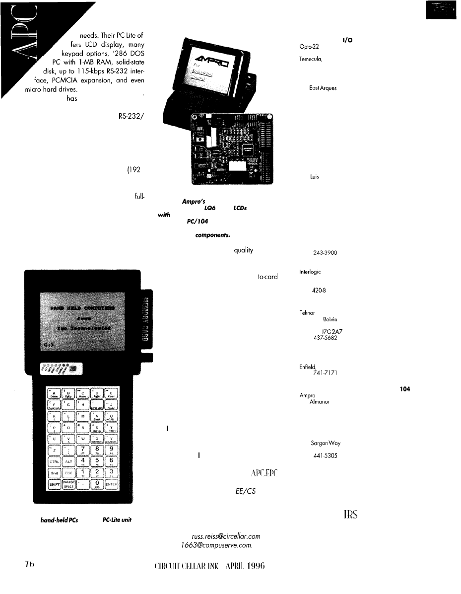
CONTACTS
Analog and Digital
Panels
43044 Business Pork Dr.
CA 92590
(909) 6959299
Fax: (909) 695.2712
Advantech
750
Ave.
Sunnyvale, CA 94006
(408) 245-8268
Fox: (408) 245.8268
LCD/Keyboard Modules
Z-World Engineering
1724 Picasso Ave.
Davis, CA 95616
(916) 757-3737
Fax: (916) 753.5141
STD Bus Card Cages and Accessories
Ziatech
1050 Southwood Dr.
San
Obispo, CA 93401
(805) 541.0488
Fax: (805) 541.5088
Kinetic Computer Corp.
270 Third St.
Cambridge, MA 02 142
(617) 547.2424
Fax: (617) 547.7266
Computer Dynamics, Inc.
16530 Commerce Ct.
Middlebury Heights, OH
(2 16)
Fox: (216) 243.3901
Industrial Rack-Mount Embedded PCs
Industries
85 Marcus Dr.
Melville, NY 1 1747
(5 16)
1 1 1
Fax: (5 16) 420.8007
Display Pack Systems
Microsystems, Inc.
616 Cure
Boisbriond, QC
Canada
(5 14)
Fax: (5 14) 437.8053
Interactive Display Systems
198 Freshwater Blvd.
CT 06082
(860)
Fax: (860) 74 l-70 17
Miniature LCD Display Modules and PC/
Computers, Inc.
990
Ave.
Sunnyvale, CA 94086
(408) 522-2 100
Fax: (408) 720-l 305
Hand-held PCs
Two Technologies, Inc.
419
Horsham, PA 19044
(215)
Fax: (215) 441.0432
Kilo Systems
2300C Central Ave.
Boulder, CO 80301
(303) 444.7737
Fax: (303) 786.9983
Kila Systems
a
similar offering touted
as a PC-in-a-Box with OEM pricing as low
as $500. This system offers three
485 serial ports, a printer port, and a
24-bit parallel port. They’re powered from
internal batteries (4-20 hours of operation)
or external DC power for extended use.
Unfortunately, the’re monochrome only
and have restricted display resolution
x
128 pixels). Of course, they only show a
portion of a conventional DOS screen. But,
it’s only a matter of time before we’ll get
color- screen, hand-held PCs.
C O N C L U S I O N S
While the form your embedded PC
takes varies tremendously depending on
your application, it’s best to consider the
options and details of packaging early in
Photo 8: Operating from batteries or a wall
pack,
like this
from
Two Technologies permit the embedded PC to
travel anywhere for on-site data entry and
collection, machine setup, data acquisition,
and other remote computing needs.
Photo 7:
Mini-LCD Adapter permits
compact Sharp
color
to
operate
their minimodule display controller. A
miniature
embedded system com-
plete with operator display can be assembled
around these
the development cycle. The
of pack-
aging affects everything that follows.
With the plethora of packaging options
available-from simple backplanes
cages, industrial boxes, complete PC-based
display systems-there is seldom a good
reason to reinvent the wheel. Investigate
several approaches and multiple vendor
offerings before deciding on this important
aspect of your embedded PC design.
TYING THE BOW
It’s
been a pleasure this past year to
introduce you to the fast growing and
exciting world of embedded PCs.
However, due to work pressures, I’m
forced to resign my position as columnist of
Applied PC. There’s much I’ve not yet
touched on, but I’m sure others will pick up
where I’ve left off.
may be back from time to time to
discuss specific topics. And, you’ll still see
my PIC projects and other INK feature
articles when can find the time to bring
them to you.
Again, it’s been a pleasure.
Russ Reiss holds a Ph.D. in
and
has been active in electronics for over
25 years as industry consultant, de-
signer, college professor, entrepreneur,
and company president. He may be
reached at
or
70054.
425 Very Useful
426 Moderately Useful
427 Not Useful
DEPARTMENTS
Firmware Furnace
Ed
From the Bench
80x86 Performance
Cache Craziness Redux
Silicon Update
ome years ago,
an innovative PC
designer came up with
a system board that
wrung incredible performance from
seemingly stock hardware. Nobody
understood quite how it worked, but
the standard benchmarks agreed that it
ran rings around the competition!
This guy [I can’t bring myself to call
him an engineer) noted that bench-
mark programs use standard PC timing
facilities. The usual approach to high
performance packs more instructions
into each second. His approach simply
made each second slightly longer..
Closer to home, when upgraded
my test system from a 33-MHz ‘386SX
to an
the Firmware
Furnace Task Switcher’s
mode performance jumped by a factor
of six. A few tests showed that the
new system’s cache memory account-
ed for essentially all of the perfor-
mance increase. A better CPU, wider
data path, and nearly tripled processor
clock mattered hardly at all!
In this column, I’ll explain why
memory limits PC performance, show
how caching can help, describe how a
Direct Digital Synthesis loop reveals
the cache in action, and present a sim-
ple circuit we’ll use next month to get
some detailed timing information.
If you’ve ever wondered how a
MHz CPU uses
DRAM, read on.
78
Issue
April 1996
Circuit Cellar INK@
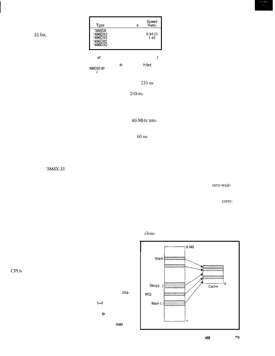
WHAT’S THE PROBLEM?
The Firmware Furnace Task
Switcher, for those of you new to the
column, is a
protected-mode,
cooperative multitasking program
I
built last year. While not a full-fledged
operating system, it exercises and
demonstrates a big chunk of the mys-
terious protected-mode hardware
found in current PCs.
When I began writing the FFTS
keyboard handler, I discovered that I
had zapped the ‘386SX system board’s
keyboard hardware sometime in the
last two years. Rather than fix it, I
simply jacked up the box and slid an-
other system board underneath. After
twiddling a pair of delay loops that
matched some peripheral gadgets to
the CPU speed, the rest of the FFTS
code worked perfectly.
After I adapted the code, I wondered
just how much difference the new
hardware actually made. Because the
FFTS kernel displays the number of
task switches per second on the video
monitor, I used that as a simple figure
of merit. Table 1 summarizes the re-
sults, with the old
setting
the performance baseline.
The second line of that table may
raise some eyebrows. The FFTS kernel
actually ran 6% slower on the new
board when I disabled both caches!
Obviously, memory performance dom-
inates everything else for this combi-
nation of hardware and software.
Enabling just the external cache
boosted task-switching performance by
more than 50%. Enabling only the
internal cache gave better results,
improving performance by a factor of
five. Running with both caches en-
abled added another 20%.
You might think that every ‘486
system should run with both caches
enabled. It turns out that not all ‘486
have the same internal cache
size, some embedded PC boards lack
external caches, and sometimes cach-
ing hurts.
But, if a six-times performance
difference doesn’t get your attention,
flip to the next column!
WHO’S RESPONSIBLE FOR THIS?
In the beginning, the Original PC
ran an 8088 CPU at 4.77 MHz. Each
C P U
Caching
S w i t c h e s
per
none
4 0 0
1 .oo
none
3 7 7
external
5 7 7
internal
2 0 6 8
5.17
both
2 4 4 4
6.11
Table l--The 80486 CPU’s internal cache contributed
heady the factor of-six performance improvement
saw when porting the protected-mode Firmware
Furnace Task Switcher the new board.
the
actually ran slower than the ‘386%33
when disabled both caches!
instruction required several
clock cycles, which quite nicely
matched the system’s
DRAM
access time. After all, when a simple
JMP took 15 cycles, waiting a cycle or
two for each memory access was no
big deal.
Today, however, an
DX2 executes that same J M P in three
12.5ns CPU clock cycles. The five
CPU cycles required for a
DRAM access look downright poky in
comparison. When the processor stalls
every time it reads or writes memory,
a fast CPU clock doesn’t buy very
much performance.
challenge. Contrary to popular belief,
just sticking fast RAM in a slow box
won’t make it go any faster.
Fortunately, most programs don’t
use all 8 MB at once. Your programs
(usually) execute a few close-together
instructions that access a few
The subject of caching would never
arise if every PC used zero-wait-state
memory. However, filling your PC
with 8 MB of blazing RAM might pose
a problem, even if your Mastercard
and air conditioner were up to the
jors call
spatial
and
temporal locality.
The former means that programs typi-
cally access memory in small, sequen-
tial areas. The latter means that, once
a program accesses an area of memory,
it generally accesses it again soon.
Obviously, those principles cannot
always be true or GUI programs would
still fit on a single diskette. Comp Sci
types refer to the collection of memory
in use at any instant as the program’s
working set.
That set changes as the
program executes different subrou-
tines, handles interrupts, and so forth.
You can think of the working set as a
small peephole sliding over your
program’s code and data.
Figure 1 shows how a relatively
small cache can hold the few sections
of main memory required at a given
moment. The working set and thus the
cache contents may be completely
different every few milliseconds as the
program moves on to new instructions
and data.
CPU must slow down for the
sponding external memory references.
Success has a simple metric: the
cache hit ratio. Because the cache
control logic cannot always predict
precisely what the program will do
next, the hit ratio must be less than
The cache, being small, can run
much faster than main memory. Ac-
cessing the cache thus imposes much
less delay on each instruction, letting
the CPU run faster. In the limiting
case, with all instructions and data in
the cache, the CPU sees
state memory. In the general case,
some accesses miss the cache, and the
together variables, most
of the time. Loops, for
example, repeatedly
execute the same in-
structions over and over
again. You don’t need 8
MB for a few dozen
instructions!
A cache depends on
two principles that
computer science
Figure
typical
program
exhibits locality of reference
because most of its memory
accesses in a few areas. A
relatively small
cache can ho/d the
programs working set, even for a
system with 8 MB of
Variables
256 KB
(
handler
.
0
DRAM
Circuit Cellar INK@
Issue
April 1996
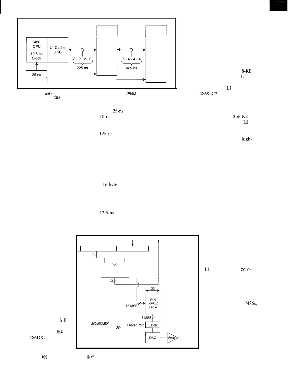
L2 Cache
256 KB
DRAM
8 M B
Clock
Figure
2-Accessing
from the external cache takes ha/f as long as reading
but whether the CPU waifs
for 425 ns or 650 ns when
isn’t in the cache depends on fhe system design. You hope for the former but may
well get the latter!
1 .OO. When the ratio falls below about
0.70, designers get worried.
As the hit ratio declines, the time
spent filling the cache with unneces-
sary data occupies memory bus cycles
that delay the proper data. For some
applications, disabling the cache actu-
ally improves the system’s overall
performance!
Collecting precise cache usage fig-
ures requires either complex CPU
simulation code or expensive instru-
mentation. While we can’t venture
into that territory, we can certainly
gain some insight into PC cache mem-
ory with the aid of some low-level
code, a few I/O bits, and nothing more
exotic than a decent oscilloscope.
First, let’s find out what we’re up
against.
CLOCKS AND CACHES
Current PC ads show
true specsmanship in
action. Numbers like 66,
75, 80, 90, 100, and 133
MHz belie the simple fact
that system-board designs
remain stuck at about 40
MHz. The CPU doubles,
triples, or quadruples the
external clock to produce
both its internal clock and
those magic numbers.
Regardless of your system,
however, the PC Compat-
ibility Barnacles and sim-
ple physics prevent a
throttle design.
For example, my
MHz
has a sys-
tem clock of 40 MHz and
thus a
basic clock cycle. It uses
DRAM, but the recommended
BIOS settings allow five cycles for the
first memory access of a burst. That
delay provides enough time to
detect an external cache miss, set up
the memory access, and fetch data
from the DRAM chips.
For reasons that we won’t go into
yet, memory accesses generally occur
in bursts of four cycles. The next three
accesses of a burst each require four
cycles or 100 ns. On the average, then,
a
access costs 26 ns per byte.
if it touches DRAM. I don’t recall
seeing those numbers in any PC ad.
However, add the numbers and
weep. Each memory access requires a
total of 17 clock cycles! An instruction
that normally completes in a few
CPU cycles must wait 425 ns
The mismatch between CPU clock
rates and DRAM access times is now
so dramatic that ‘486 and Pentium
systems sport tandem caches. A pri-
mary, internal cache on the CPU chip
provides zero-wait-state access, while
a secondary cache on the system board
reduces the effect of slow DRAM on
the primary cache.
The Intel ‘486 series has an
internal cache, also called the
cache. Other vendors have different
opinions of the proper cache size:
the IBM
has 16 KB while the
Cyrix ‘486SLC has only 1 KB. Don’t
look for those numbers (at least the
smaller ones!) in the ads either.
My system board has a
secondary cache, known as the
cache. You’ll find L2 options ranging
from zero on some embedded systems
to half a megabyte or more on
end PC boards. As with internal
caches, the effect depends on your
application.
The default BIOS settings for the
external cache on my board allow
three cycles for the first access of a
burst and two cycles for each of the
remaining three accesses. This works
out to 225 ns total or 14 ns per byte.
The system board specs don’t reveal
whether the external cache copies
incoming DRAM data while passing it
directly to the CPU. If so, the CPU
Phase Increment
Phase Accumulator
32
Adder
Figure 3-A
Direct Digital
Synthesis loop produces an
analog output from a tab/e of
values addressed by a
Phase
The
lookup fable with 16,384
bit entries holds enough
data to stress the cache and
is gross/y oversized for
normal applications.
Analog
Output
waits only 425 ns. If not, missing both
caches costs 425 ns while the external
cache fills, then 225 ns to
load the internal cache. In
other words, there’s 650 ns
of pure, unadulterated
delay!
Figure 2 shows the lay-
out of the two caches. The
cache can offer
wait-state access because it
lives on the same chip as
the CPU. The L2 cache,
while dramatically slower,
provides data at twice the
speed of DRAM. For
all data transfers occur four
bytes at a time, with four
transfers in each burst.
Most PC references
simply advise you not to
worry about caching, be-
cause you can’t control it.
80
Issue
April 1996
Circuit Cellar
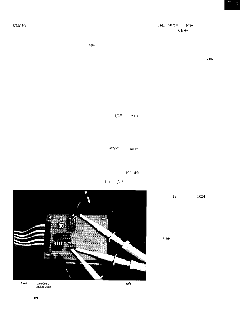
Color me paranoid, but I want to know
more about anything that drags an
CPU to a crawl.
Don’t you!
DIRECT DIGITAL SYNTHESIS
Although the FFTS kernel provides
a dramatic introduction to the subject,
it is neither convenient nor particu-
larly adaptable for our purposes. I de-
cided to write a small test routine that
exercises the cache under carefully
controlled conditions.
You have surely seen DDS (Direct
Digital Synthesis) described elsewhere,
probably in the context of generating
good sine waves with fine frequency
control. I’ve perverted the idea into a
cache exploration tool.
Engineers generally implement
DDS in hardware because the algo-
rithm requires very little control logic.
Figure 3 shows the basic idea: add an
increment to a phase accumulator that
addresses a table. Each pass through
the table produces a single cycle of the
output value, with the frequency de-
termined by the size of the increment.
Notice that the phase increment
and accumulator registers have many
more bits than needed to address the
output lookup table. This overkill
allows phase increments much smaller
than a single output step and gives the
DDS very fine frequency resolution.
The lookup table’s width has no
relation to its number of entries. You
can have a tall, skinny table or a short,
fat one. You can produce a respectable
analog output from an g-bit-wide table
and get an excellent waveform with 16
bits. The system’s amplitude resolu-
tion
determines the table width
and its frequency range sets the length.
A normal DDS loop produces out-
put values based on a fixed timing
reference. Each clock tick latches a
new (increment + phase) value into the
phase accumulator register and sends a
new table output to the DAC. The
output frequency equals the clock
frequency times the phase increment
divided by the maximum possible
phase increment.
For example, had I written the DDS
loop to produce one output value on
each BIOS tick, the lowest frequency
would be 18.2 Hz x
= 4.2
Yes, 4 nanohertz. One cycle every 2.7
days. Good for timing glacier races.
The highest frequency depends on
how ugly a sine wave you can tolerate.
Assuming you can stand 32 outputs
per cycle, the BIOS-ticked loop would
run at 18.2 Hz x
= 586
Yes, half a cycle per second.
Microcontroller applications that
need a fairly low output frequency can
use DDS loops. Suppose you updated a
16-bit accumulator with a
interrupt. The minimum frequency
would be 100
x
or about
Photo
custom
provides convenient access to the PC
parallel-port signals we use
investigating cache
82
Issue
April 1996
Circuit Cellar INK@
1.52 Hz. The maximum, again assum-
ing 32 outputs per cycle, tops out at
100
x
or 3
The DDS
loop gives you a
sine wave that
you can adjust in 1.5Hz steps.
Now you can see why real DDS
loops require hardware registers with
fast clocks.
Homework: figure the output fre-
quency range and resolution for a
MHz clock applied to 32-bit increment
and accumulator registers.
Hint: check the Analog Devices
AD9950 DDS Phase Accumulator chip
for more details. The state of the art
moves right along, but only ECL logic
can keep pace!
You must use a fixed clock to get a
known output frequency regardless of
the code’s execution time. In my test
code, however, I simply let the DDS
loop run as fast as it can, updating the
phase accumulator and producing
output values whenever it can. Given
a fixed CPU clock and no other dis-
tractions, the update rate depends on
the DDS loop’s execution time.
Here’s the punch line: the DDS loop
executes faster when it accesses data
in the CPU cache. By watching the
update rate on a scope, we can detect
cache misses as they occur. By adjust-
ing the phase-increment step size, we
can control the amount of data passing
through the cache and, thus, the cache
hit ratio.
More homework: what cache hit
ratio would you expect with a phase
increment of What about
Hint: your first guess is probably
wrong, but I haven’t given you quite
enough information to solve the prob-
lem yet.
THE HARDWARE CORNER
Although we’ll deal primarily with
the loop’s low-level timing, I built a
simple
DAC circuit that gener-
ates an analog output voltage. A PC
printer port has (barely) enough bits to
drive the DAC, produce a few timing
signals, and read a few DIP switches.
Every PC has a printer port, however,
which means we can concentrate on
code rather than hardware.
Figure 4 details the minimal cir-
cuitry and port connections. Photo 1
gives you an idea of the layout on a
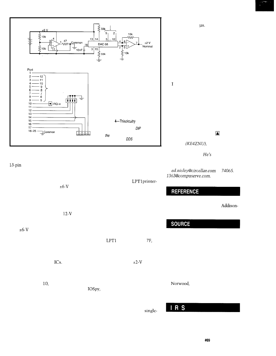
12 VDC
Battery
Printer Port
_
-6 V
Op Amps: LM324
Printer
DAC 08
DIP Switches
Output
Test Points
Figure
converts fhe
digital value from the lookup table into
an analog voltage. The
switches
select various phase
increments and
output bits monitor events
occurring in the
loop code.
2.5” x 3”
Radio Shack perfboard. I used
For this application, the additional
shielding in a round cable makes no
difference.
a ribbon cable crimped between a 2 x
socket and a DB-25F connector.
good news is, as long as you follow the
schematic, everything works OK.
control port at (base + 2). Check your
references for the details of which bits
have what polarities in each port. The
The BIOS stores the
port base address in the word at 0040:
0008. The more-or-less standard value
is 0378 hex, but you may find 03BC or
0278, depending on the hardware in
your PC. When you write your own
programs, use the BIOS address rather
than hard-coding an assumption that
works on just your PC.
A 12-V battery provides
power
for the circuit, with an LM324 op-amp
driving the centered common (ground)
voltage. This technique works well for
the single milliamp required by this
circuit.
I
happened to have a
sealed lead-acid battery on my desk
and a quad op-amp in the parts box,
but a
split supply works as well.
You must, however, connect at
least one printer port ground pin to the
analog common voltage. Don’t short
either side of the battery to the port’s
ground connection, lest you release the
magic smoke inside the
A four-position DIP switch sets the
printer port’s four status input pins.
My DDS code doesn’t, use the port’s
IRQ signal on pin but you may as
well wire it to a terminal. I connected
the port’s four output pins plus the
IRQ signal to a five-pin terminal strip.
They’re not the best scope probe test
points, but they work well enough.
The digital input bits from the DIP
switch appear in the printer status port
at (base + 1). The output bits are in the
Hardware checkout shouldn’t re-
quire much effort. I used DOS Debug
to set the
data port to 00,
and
FF and a voltmeter to verify the corre-
sponding minimum, midrange, and
maximum output voltages. The cir-
cuitry I used produces a
output.
Debug also sets the control bits and
displays the status bit, albeit with less
convenience than you’d like. The disk
with The Undocumented PC includes
a TSR that monitors and dis-
plays PC I/O ports. I watched the bits
flip as I toggled the DIP switches,
which made life much easier.
If your parts box includes a
supply DAC and op-amp, the design
may be even simpler. There are no
critical timing specs, as the software
DDS loop produces a new output value
roughly every 10
The output table I
used presumes the DAC accepts raw
binary coding.
In a real DDS application, you must
pay much more attention to the analog
circuitry. What you see in Figure 4
provides a quick-and-dirty look at the
sine output. It is certainly not the final
word on the subject!
RELEASE NOTES
can’t release the code implement-
ing the DDS loop until I have room for
the caveats. Believe me, it is a truly
hostile beast. Most programs don’t
disable all interrupts and shut off RAM
refresh, but that’s what we need for
precise timings.
Next month, we’ll take a look at
the DDS software and probe ‘486 cache
behavior in serious detail.
Ed Nisley
as Nisley Micro
Engineering, makes small computers
do amazing things.
also a
member of Circuit Cellar INK’s
staff.
You
may reach him
at
or
Van Gilluwe, Frank.The Undocu-
mented PC. Reading, MA:
Wesley, 1994. ISBN o-201-62277-7.
Analog Devices sells their data
manuals and app notes through
their literature hotline. If you in-
tend to do DDS right, get their Data
Converter Reference manuals and
the System Applications Guide.
Analog Devices
One Technology Way
P.O. Box 9106
MA 02062-9 106
(617) 461-3392
Fax: (617) 821-4273
428 Very Useful
429 Moderately Useful
430 Not Useful
Circuit Cellar INK@
Issue
April 1996
83
Jeff Bachiochi
Finally Fill the Rainbow
money mongrel Mr. Pot-
ter in the high school’s rendition of
a Wonderful Life.
The original movie,
starring Jimmy Stewart and Donna
Reed, was filmed in black and white,
as were all movies until color was
introduced during the filming of The
Wizard of Oz.
Deeming it too expen-
sive to reshoot the beginning Kansas
scenes, the directors left them as black
and white, while everything in Oz is in
splendid
As it turned out,
the split is an artistic quirk of fate.
Wheeler-dealer Ted Turner has
funded the coloration of many older
black-and-white films, including
a
Wonderful Life.
Luckily, he balked at
Oz.
I watched many a television show
in black and white. And, although I’ve
shared years of Sesame Street with my
kids, I was raised on Ding Dong School
(with Miss Francis).
Anyone else cultivated on
and-white programming knows how
living in full color helped one imagine
in the grays. The perception of black
and white is a bit different for those
raised strictly on color programming.
Photography has gone through the
same transformation. Early
white photos were developed on glass,
metal, and finally paper.
The introduction of Kodachrome
has all but wiped out black-and-white
photography. Still, to many profes-
sional photographers, black and white
continues to be the medium of choice.
If all this seems a bit outdated, look
at laptops. The relatively new
screen technology has brought full
color to
and led to the
computer revolution. Flat-panel,
screen, high-definition LCD TVs are in
our not-too-distant future.
The last hurdle preventing
color
is now being cleared. Even
though blue
were actually an-
nounced years ago, it took a hefty
wallet to purchase one until recently.
One of the first available to you and
me is a multicolor LED. In reality, it
has four
on the same substrate:
one red, one yellow, and two blues.
ELECTROMAGNETIC RADIATION
The limits of the electromagnetic
spectrum extend from audio to cosmic
rays. See Table 1 for a view of the
electromagnetic spectrum.
Of all the frequencies we are bom-
barded with each day, the narrow band
from 430 to 750
is of most impor-
tance to our limited bodies. We receive
the majority of our everyday reality
from this otherwise insignificant slice
of the universe’s spectrum.
The magic of the rainbow begins
with the color red at a wavelength of
about 700 nm, and continues with
orange (620 nm), yellow (580 nm),
green (520 nm), blue at (420 nm), and
violet (400 nm).
500
600
700
Wavelength (nm)
Figure l-Our eyes are most sensitive green and
yellow light
the tip of the
be//-shaped curve) as
opposed to red or violet, which
are located near the
ends of the curve as depicted here.
84
Issue
April 1996
Circuit Cellar
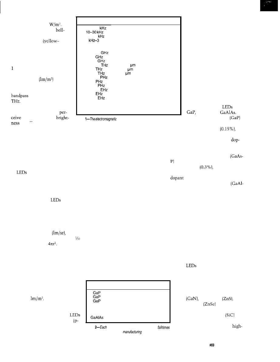
The radiant energy of this
light is measured in
However, the eye has a
shaped sensitivity curve which
peaks at 555 nm
green).
Therefore, the actual bright-
ness as seen by the eye de-
pends on the frequency. Figure
offers a graph of photopic
luminosity in lumens per
meter squared
versus
color (wavelength).
This function is similar to a
filter centered on 540
It means our eyes need to
receive higher radiation densi-
ties of reds and violets to
Freauencv
16 Hz-l 6
30-300
300
MHz
3-30 MHz
30-300 MHz
300 MHz-3
3-30
30-300
300 GHz-3
3-30
30-300
300 THz-3
3-30
30-300
300 PHz-3
3-30
30-300
Wavelength
Name
Audio Frequency
30-l 0 km
Very Low Frequency
10-l km
Low Frequency
1 km-100 m
Medium Frequency
100-10 m
High Frequency
10-l m
Very High Frequency
1 m-100 mm
Ultra High Frequency
100-10 mm
Super High Frequency
10-l mm
Xtra High Frequency
1 mm-100
100-10
10-l
1 pm-100 nm
Visible Light
100-10 nm
X-rays
10-l nm
1 nm-100 pm
100-10 pm
10-l pm
Gamma rays
1 pm-l 00 fm
100 fm-10 fm
Cosmic rays
10-l fm
as yellows and
greens.
If we assume a point light
them at the same
Table
spectrum as we know if today contains some
interesting names. The frequency and wavelength of visible light is highlighted.
source, we can count the number of
lumens which fall on the area of a
sphere surrounding it. By comparing
the power used by the source to the
total lumens falling on the surface of
the sphere, we get an idea of the effi-
ciency of the source.
don’t generally expend their
light uniformly in all directions.
Therefore, luminous intensity must be
measured and graphed with reference
to its axis of symmetry, either vertical
or horizontal. (Some
don’t have
an axis of symmetry, but I’ll leave that
for another day.)
The number of lumens falling on an
area of the sphere equal to the radius
of the sphere squared is known as the
lumens per steradian
or can-
dela (Cd), which is actually about
the sphere’s area of
In Figure 2, the candela is graphed
in relation to the center axis of a typi-
cal LED. Maximum candela is refer-
enced as 1 .O. This spatial distribution
pattern depends on the lens system
used by the LED.
The material with extra electrons is
considered to have a negative charge
(n-type) while the material with an
electron deficiency has a positive
charge (p-type). A p-n junction is
formed when n- and p-type materials
are combined. The extra electrons and
holes attract one another, which cre-
ates a current flow in the forward-bias
direction and prevents reverse flow.
Not only does the material used
affect the wavelength of the color
emitted, it also affects the rise and fall
response time (see Table 2). This varia-
tion is of concern to those interested
in fiber optics. Notably, the efficien-
cies given above also vary based on
manufacturing process.
ENTERTHEBLUES
Because the gallium materials used
in these
don’t have the potential
for emitting higher wavelengths (the
blues), other materials have been
Video cameras today are rated in
investigated.
lux, which indicates ‘the sensitivity
Material
Color
Rise Time
Fall Time
Although initial results showed
of the CCD receiver. One lux is
red
700 ns
3000 ns
yellow-green
800 ns
promise, research into gallium ni-
equal to 1
700 ns
green
50 ns
400 ns
tride
zinc sulfide
and
GaAsP
P-N JUNCTION
red
200 ns
150 ns
zinc selenium
was discontin-
GaAsP
orange
300 ns
220 ns
ued for practical reasons. It was
Like semiconductor diodes,
GaAsP
yellow
300 ns
220 ns
are made up of positive-negative
red
40 ns
60 ns
found that silicon carbide
had
the most favorable manufacturing
n) junctions. The base material has
Table
color of LED exhibits different rise and
characteristics, as well as the
an outer electron shell that is not
which depend on the LED’s
process,
est
conversion efficiencies.
When a free electron re-
combines with a free hole,
radiant energy is released
equal to the difference be-
tween the two carriers prior to
recombination. The wave-
length of the emitted energy
varies with the potential dif-
ference and the material used.
If the emitted wavelength
falls within that of visible
light, an LED is born.
LIGHT-EMITTING
MATERIALS
The most common materi-
als used in today’s
are
GaAsP, and
Gallium phosphide
is
capable of emitting red (4%
efficiency), green
or
complete on its own. Thus, outer-shell
yellow-green (0.3%). The emitted
electrons can be shared between adja-
wavelength is controlled by the
cent atoms (covalent bonding) and
ants: zinc and oxygen for red and nitro-
form crystalline structures.
gen for yellow-green.
In this form, the materials are non-
conducting because all atoms have full
outer shells. However, by adding an
atom of an element with one less elec-
tron (the element one lower than the
base element in the periodic table), a
crystalline structure is created with a
missing electron (or an extra hole).
Similarly, if an atom with an extra
electron is added to the base material,
the crystalline structure contains an
extra electron.
Gallium arsenide phosphide
is capable of emitting red (4% effi-
ciency), orange
or yellow
(0.12%). Again, nitrogen is used as a
for orange and yellow.
Gallium aluminum arsenide
As) is capable of emitting red. It has
the highest luminous efficiency, about
15%.
Circuit Cellar INK@
Issue
April 1996
85
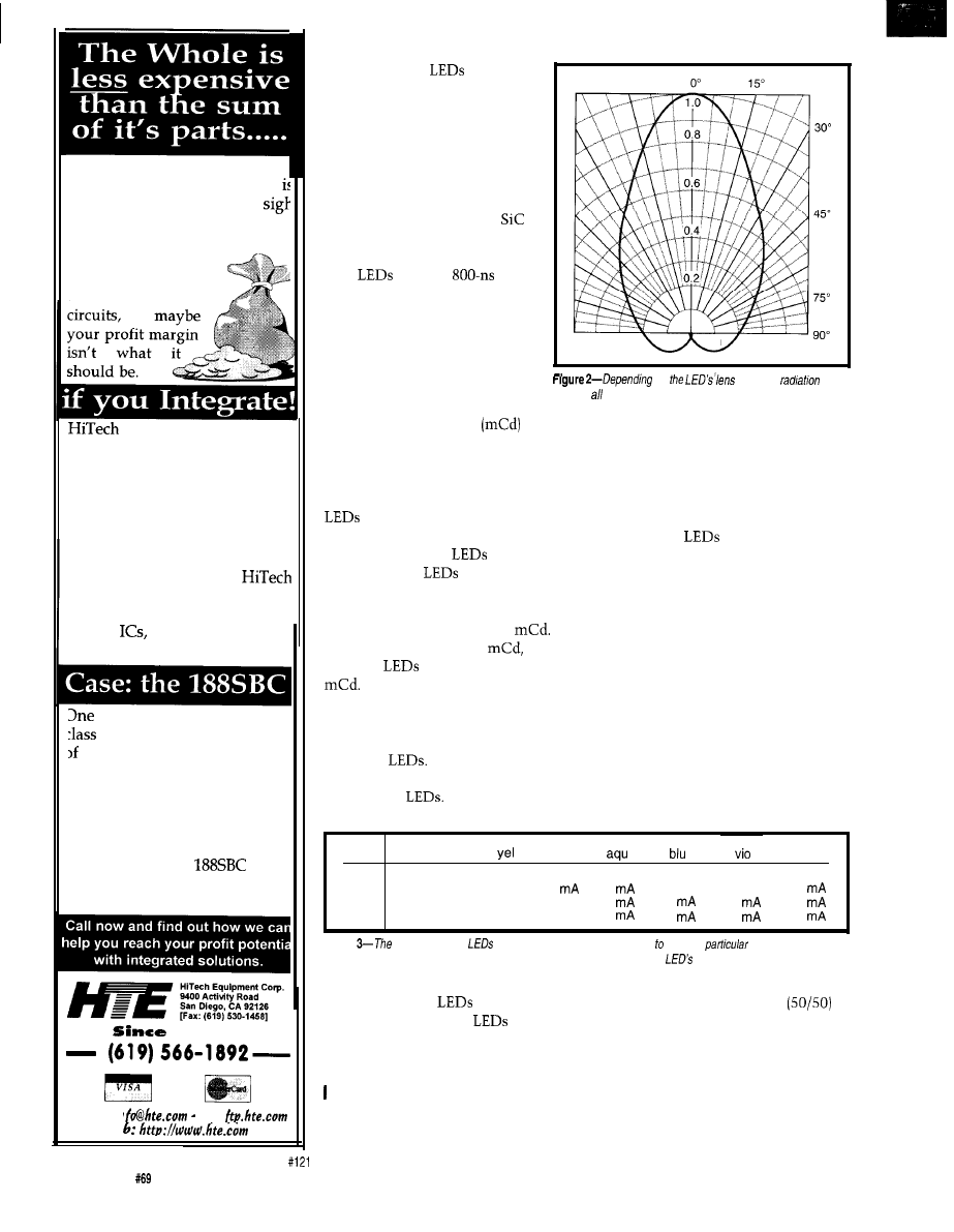
You’re shipping the first system:
out the door, the customer
happy, and you can breath a
of relief now, right? But can you
really afford to relax now?
If that system was
built using
many
different boards and
can combine all those
boards and circuits onto a single
board, saving you big money.
Reduce your unit cost with less
inventory and fewer vendors,
faster assembly time, fewer ca-
bles, and even smaller package
size. Built to your specifications,
an integrated board from
can include analog, digital,
FPGA and even custom mixed
signal
all for less money
than your current solution.
customer needed an x86
processor with 16 channels
12 bit A/D and 8 channels of
12 bit D/A, LCD, Keypad and
Opto-rack interface, two serial
ports, a printer port, real-time
clock, and more. A multi-board
solution would cost around
$1200 each. The
costs
only $749, and includes a power
supply and a custom FPGA!
1 9 8 3
V
A
E-mail: in
Ftp:
We
For the blue
as with
the others, p- and n-type materi-
als are produced by doping the
base material with tiny bits of a
material that has more or fewer
electrons in its outer shell.
Adding aluminum to silicon
carbide produces the p-type
region, and nitrogen to the
produces the n-type material.
The switching speed of the
blue
is in the
range. Efficiency is lacking. Not
only is the dominant wave-
length beyond that of the visual
spectrum, but the blue end of
the visual spectrum, like the red
end, is not as sensitive as the
green-yellow peak. Therefore,
on
makeup,
IS
not
equal in directions.
6 0 ”
very small millicandela
output
is typically produced.
THE MULTICOLORED LED
By packaging red, green, and blue
in a single package, white light
(as well as all the other colors) can be
emitted. Since blue
are so ineffi-
cient, two blue
are included with
a single red and green.
The red LED has the highest output
efficiency-it can produce 12
The green can produce 2
but the
two blue
together output only 1
Table 3 lists the currents that
each LED requires to produce the com-
plete spectrum of visual light.
Notice the high currents needed in
both blue
This requirement
demonstrates the low efficiencies of
today’s blue
In addition, while
ries-dropping resistor which limits the
current, based on your VCC. It’s not a
big deal for single-color operation.
By placing a switching transistor in
the circuit (one per color), you can add
digital on/off control for each color.
The two blue
can be run from
the same transistor, provided that each
has its own series-dropping resistor.
Choose a series-dropping resistor
that provides the maximum current
(see Table 3) for each color. By biasing
the transistors either on or off, you can
satisfy many combinations simply
with maximum or minimum (zero]
current.
This static state doesn’t offer much
control without operating the transis-
tors in their linear region. Digitally,
you can acquire that kind of analog
control with much simpler circuitry. If
LED
red
org
grn
wht
red
5 m A
5 m A
5 m A
0
0
0
5 m A
5 m A
green
0
1 2 m A
3 0 m A
20
2 0
0
0
20
blue1
0
0
0
0
3 5
3 5
35
35
blue2
0
0
0
0
3 5
3 5
35
35
Table
different-colored
require different amounts of current produce
colors. The current
required depends on both fhe LED efficiency and the eye’s
sensitivity to
fhe
color.
the red and green
have a forward
drop of about 2 V, blue
require
about 3.5 V, so they’re not appropriate
for 3-V systems.
you bias the transistor with a
square wave and use a frequency high
enough to eliminate any visible flick-
er, the LED is perceived as dimmed
(operating at a lower current).
SEE THE LIGHT
This method is used with multi-
To operate a multicolor LED in any
plexed displays to increase peak cur-
one color, choose the appropriate se-
rent while keeping the average current
86
Issue
April 1996
Circuit Cellar INK@
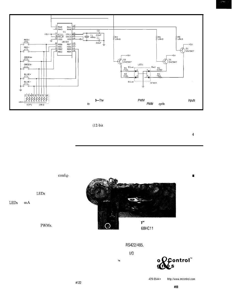
down. In this application, I vary the
TRI-PWM CONTROL
increase or decrease the three PWM
on- and off-time of each cycle to adjust
The micro’s code takes up around
percentages.
the average current through each LED.
100 words
instructions). This
The real-time clock/counter
By increasing on-time, the average
code includes generation of a master
(RTCC) is initialized with a prescaler
current and luminosity go up to 100%.
oscillator with three PWM outputs.
to create a clock tic about every us.
By decreasing it, the average current
Six push buttons (two for each color)
The master PWM frequency is set by
Figure
microcontroller produces three
signals which control three LED colors.
the micro independently increase or decrease each
duty
and luminosity go down to 0%.
This type of PWM control is widely
used in the control of DC motors. To
create three PWM outputs, I used an
inexpensive microprocessor.
Refer to the schematic in Figure 3.
Here, six push buttons are connected
to one of the micro’s ports and
ured as inputs. The remaining port is
configured as outputs which bias the
three LED drive transistors. Some
micros can drive
directly, but
not to the extent necessary for the blue
(35
each).
When you don’t have time
to reinvent the wheel
n n n
An alternate circuit might use four
LMC555 timers. The first creates a
stable oscillator, which is fed into the
trigger inputs of the remaining three
‘555s configured as
The control
inputs of each PWM come from three
potentiometers. The PWM outputs
provide the bias for each of the LED’s
transistor drivers.
There is an advantage to using a
micro in the investigation of the mul-
ticolor LED. Although both circuits
enable the user to raise and lower the
light levels of each LED, the circuit
using the micro can be easily altered
through software.
The “Small-l measures only 3.5” x 4.5”
l
Motorolla
processor offers familiar
Eliminate
programming and bullet-proof reliability
l
8K battery-backed RAM
l
Watchdog timer
the time and
l
Up to 32K on board memory
l
Real-time clock
hassle of
l
and dual-RS232 ports
extra design
l
Keypad and LCD interfaces
l
Expansion bus
turns with the
to interface
l
Single 5 volt supply
Small-l 1
controller
Micro
D i a
t i c s
Micro Control & Diagnostics, LLC
300 Main St., Suite 201, Lafayette, IN 47901
Phone:
(800) 429-6797
or (317) 429-6777
l
FAX (317)
Web:
Circuit Cellar INK@
issue
April 1996
87
writing a value of
to the RTCC
and waiting for it to roll over (once
every 25 tics). One output cycle equals
100 rollovers (10 ms). Each cycle has
100 equal parts, so the PWM control is
equal to 1 in 100 parts (1%).
Our reaction time is far slower than
that of a loop time (RTCC rollover =
100 us). To prevent a button push from
being sampled and action taken too
quickly, buttons are only sampled
once every cycle (10 ms).
A button must be sampled 8 times
(80 ms) before action is taken. This
procedure slows actions to a reason-
able level.
The two buttons associated with
each color increment and decrement a
PWM value associated with that color.
The value can range from 0 to 100
percent. Each time the master PWM
count rolls over, all the outputs are
cleared. Each time the master PWM
count is incremented, it is compared
to each of the color’s PWM values.
When a match occurs, the associ-
ated output is set high, turning on the
LED. If the color’s PWM value is low,
its off-time is short because a match
with the master’s PWM count is made
early. If a color’s PWM value is high,
its off-time is long.
Three colors, three independent
values, and three independent PWM
outputs produce about a million color
combinations. Once you’ve been
through all of them, you’ll probably
want to take this a step further.
How about reprogramming the
micro to pick pseudorandom values for
each of the three colors?
You’ll be able to generate more
colors than the old NBC peacock ever
did. Although the LED, like that pea-
cock, has been around for many years
now, it is finally here in living color.
Jeff
Bachiochi (pronounced
AH-key”) is an electrical engineer on
Circuit Cellar INK’s engineering
staff.
His background includes product
design and manufacturing. He may be
reached at
Bueche, F. Principles of Physics.
McGraw-Hill, USA, 1965.
Bliss, John. “Theory and Charac-
teristics of Phototransistors,”
Motorola Optoelectronics Device
Data, Ap. Note AN440. 1989.
Smith, George.
and Pho-
tometry,” Siemens Optoelectronics
Data Book, Ap. Note 1. 1993.
Weyrich, Dr. Claus. “Blue-Light
Emitting Silicon-Carbide
Materials, Technology, Character-
istics,” Siemens Optoelectronics
Data Book, Ap. Note 31. 1993.
CREE
multicolor LED
Corp.
P.O. Box 677
Thief River Falls, MN 56701
(218) 681-6674
Fax: (218) 681-3380
Microchip Technology, Inc.
2355 W. Chandler Blvd.
Chandler, AZ 85224-6199
(602) 786-7200
Fax: (602) 899-9210
Motorola Optoelectronics Device Data
Motorola Literature Distribution
P.O. Box 20912
Phoenix, AZ 85036
(602) 952-4103
Fax: (602) 952-4067
Sharp Optoelectronics Data Book:
Visible Light Emitting Diodes
Sharp Electronics Corp.
Microelectronics Group
5700 NW Pacific Rim Blvd., Ste. 20
WA 98607
(206) 834-2500
Fax: (206)
Siemens Optoelectronics Data Book
Siemens Components, Inc.
Optoelectronics Div.
Homestead Rd.
Cupertino, CA 95014
(408) 257-7910
Fax: (408) 725-3439
431
Very Useful
432 Moderately Useful
433 Not Useful
First in performance
n n q n
First to market
The
Controller
l
XA operates up to 30 MHz,
yet remains 8051 compatible
program address space
l
Pipelined architecture
leaves 8051
boards in the
dust, without
time-consuming
source-code
rebuilds
Phone:
(800) 429-6797
or (317) 429-6777
l
FAX (317)
l
64K battery-backed RAM
l
Expansion bus to I/O interface
l
Real-time clock and watchdog timer
l
and RS232 serial ports
l
Available expansion modules, develop-
ment software, and other accessories
l
Custom-engineered solutions
Micro Control Diagnostics, LLC
300 Main St., Suite 201, Lafayette, IN 47901
Circuit Cellar INK@
Issue
April 1996
89
Fuzzy
PID-Pona
Tom
t o
disclose the gory technical details
(such as the type and performance of
sensors) that distinguish pipedreams
from purchase orders.
67) through its paces in an actual de-
and put the AL220 (INK
sign.
The goal is to cut through all the
snake-oil test.
Without even getting to the issue of
whether R.A.P. and I agree on the
subject of fuzzy logic itself, I certainly
concur with his complaints about
dubious marketeering. I hope this
article, with real hardware addressing a
nontrivial problem, passes the R.A.P.
PID-PONG MACHINE BASICS
Readers of the earlier articles will
hype, hope, and hoopla of fuzzy and
decide once and for all if it is good (i.e.,
worthy of consideration for main-
stream designs and applications).
In “Third Thoughts on Fuzzy Log-
ic” (IEEE Micro, August 1995,
well-known fuzzy skeptic Robert A.
Pease notes that most technical papers
on fuzzy logic “are written in esoteric
symbols and couched in obscure,
scholarly phraseology.”
Fortunately, for R.A.P. and other
like-minded pragmatists in the audi-
ence, the only thing I ever write with
“esoteric symbols” is a C program, and
long-time readers certainly know that,
when it comes to phraseology, you can
count on me to eschew obfuscation.
He also writes that such papers
usually “show trivial or ‘toy’ exam-
ples.”
I have to admit the PID-Pong ma-
chine (Photo 1) has certain toy-like
qualities. Notably, when I carried one
into the local Shlep Ship delivery
franchise, a gaggle of kids surrounded
it while the parents shrunk back. Is
that the definition of a good toy or
what?
While it’s true the PID-Pong ma-
chine is quite fun, it also proves a
surprisingly tough challenge for a con-
troller. Indeed, since the original ar-
ticle
Challenge,” INK 42
incarnations of the machine have
popped up at various trade shows and
conferences. R.A.P. accepts the
note from Photo 1 that the PID-Pong
machine has undergone quite a make-
over. I’ll be the first to admit that my
previous machines, featuring tape as a
primary construction material, could
hardly be classified as robust or even
presentable. So, this time around, I
solicited the assistance of a mechani-
cally enabled colleague (thanks go to
Jim
for a much nicer version.
Having built a few machines myself
and walked a number of other people
through it, I’ve learned there are a
number of traps and pitfalls for the
unwary. I’m trying to persuade Jim to
make the various bits and pieces of the
PID-Pong machine available for those
of you more interested in controlling
the machine than building and debug-
ging it.
Nevertheless, remembering
admonition to open the kimono, here’s
everything you need to know about
building your own PID-Pong machine.
As shown in Figure 1, the machine
relies on the popular Polaroid
ultrasonic transducer to determine the
ball’s position. Just like the “sonar” in
old war movies, the transducer sends
out a “ping”
burst) and lis-
tens for the echo.
Multiplying the delay between ping
and echo by the speed of sound and
dividing by two yields the distance.
The
with
accuracy up to
is widely used in autofocus cam-
eras, collision avoidance (e.g., RV
90
Issue
April 1996
Circuit Cellar INK@
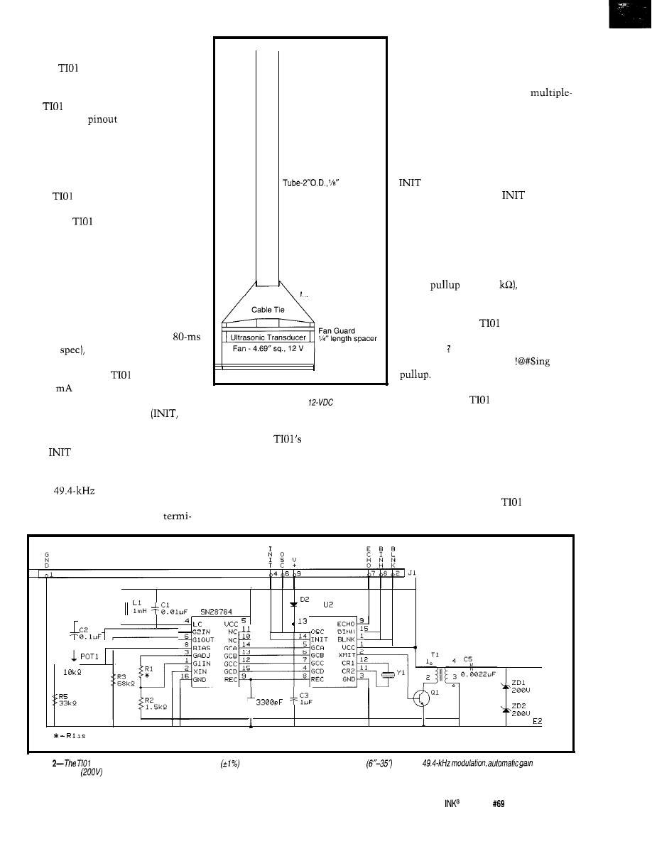
backup alarm), electronic tape mea-
sures, and the like.
The
(see Figure 2) uses seven
positions of a nine-pin connector.
Notice that somewhere along the line,
the
pin assignment seems to have
changed (this
is for a part num-
ber 615077).
Tip 1: Check your module’s pin
assignment carefully to avoid an ugly
debug session.
Starting with power, the good news
is the
can handle anything within
4.5-6.8 V. The bad news is, when it
pings, the
calls for a whopping 2
A, which is not unexpected, consider-
ing it’s really just a very tweety tweet-
er demanding a hi-fi-like 10 W to be
heard.
Tip 2: Make sure your +V is up to
snuff.
Depending on the duty cycle (which
shouldn’t be more than about 10 pings
per second to meet the module’s
recycle
you can get away with a
smaller power source using a suitable
capacitor since the
power drops
to 100
when it isn’t pinging (i.e.,
when it’s listening for the echo).
The remaining five lines
ECHO, BINH, BLNK and OSC) com-
pose the digital interface. Of these,
only
(ping] and ECHO are manda-
tory in most cases.
For reference, the OSC output is a
spare
clock for external use,
typically to drive a counter. BINH
(Blanking Inhibit) causes early
thick
3 ft. (min.) length
Manifold (e.g., ice bag)
6 W, 100 CFM (min.)
Fan Guard
Figure
l--The P/D-Pong machine relies on an
ultrasonic
transducer and a 4”
fan to test fhe
mettle of
would-be controllers.
nation of the
built-in automatic
blanking since the TIO 1 must suppress
the input for a short time after trans-
mission, lest it hear itself ringing.
In fact, it’s highly recommended
you get a small
test program or
jig working to your satisfaction before
you lash the whole machine together.
Verify that distance changes are accu-
rately detected and that there aren’t
any glitches or dropouts in the dis-
tance readings.
The blanking interval dictates the
Tip 5: Ensure there’s a good ground
minimum distance that can be mea-
and cable between the
and the
sured, with about 16” being the de-
controller to avoid false echoes.
fault. Past experience indicates that
BINH can be used. But in this applica-
tion, it only cuts the minimum a little
(to perhaps 12”).
BLNK is associated with a
echo feature, which clearly isn’t need-
ed or desired in the PID-Pong applica-
tion.
Tip 3: Remember to ground BINH
and BLNK if you aren’t using them.
Most of the action centers around
and ECHO, and it couldn’t be
simpler-just drive the
input
high and measure the elapsed time
until ECHO goes high, as indicated in
Figure 3. Well, actually it could be a
little simpler, say along the lines of
TTL compatible.
Turns out the ECHO output may
need a
(e.g., 4.7
depending
on what it’s connected to. How many
hours have been spend debugging an
otherwise perfect
setup whose
ECHO output was a few millivolts shy
of a full 1 Too many, I know..
Tip 4: Don’t forget the
“1
TL851
F I L
7
1 0
6
E l
OXDCR
c 4
OGND
s e l e c t e d a t t h e f a c t o r y
Figure
hand/es the low-level details of accurate
measurement across an extended range
including
control,
and high-voltage
transducer drive. Note that some modules have differenf pin assignments and connectors.
Circuit Cellar
Issue
April 1996
9 1
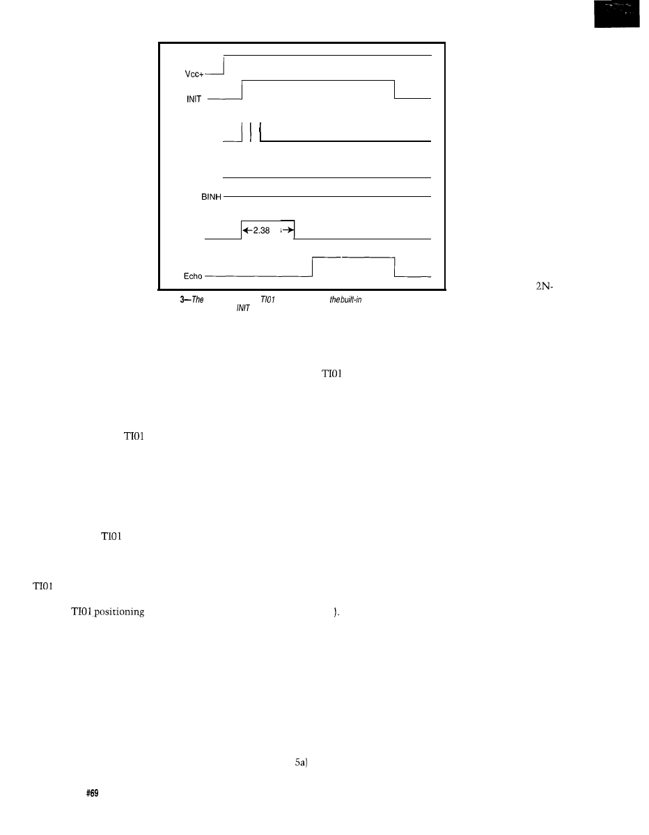
This is also a chance
to verify your driver
software. For instance,
the test program I used
indicated a distance read-
ing glitch every now and
then. At first glance,
these blips appeared to be
electrical problems like
those associated with
failure to properly heed
Tips 4 and 5.
Fortunately, I noticed
a periodicity not seen in
the typical noise-related
interference. It turns out
that the real-time kernel
on the SBC I used inter-
rupts the test program to
update its tic counter, a
distraction dispensed
with by disabling inter-
rupts altogether.
Transmit
16 Pulses
(Internal)
BLNK
Low
Low
Internal
Blanking
ms
Figure
simplest mode of
operation exploits
blanking feature to reduce
the interface to two fines,
and ECHO.
Tip 6: There’s nothing worse than
debugging hardware (that probably
actually works) with software that
doesn’t work, especially if you don’t
know it doesn’t work. Vet your soft-
ware thoroughly, so you don’t stumble
blindly if (more like, when) something
goes wrong.
With a rock-solid
interface,
the only other critical step is position-
ing the sensor relative to the bottom of
the tube. The dilemma, illustrated in
Figure 4, is that the sensor starts to
deliver false echoes if it’s located too
far below the tube.
On the other hand, if it’s too close
to the tube, the
physically im-
pedes air delivery, resulting in severe
power loss and turbulence. Using your
own test setup, verify the limits of
positioning (typically about
1”)
and mount it accordingly.
Tip 7:
and align-
ment is critical.
Another aerodynamic foible ex-
plains the machine’s open-frame con-
struction. It turns out that the airflow
is noticeably degraded by any obstruc-
tions around the fan.
Tip 8: Leave lots of breathing room
for the fan, and why not throw in a
finger guard for safety’s sake?
Once you’ve got the machine com-
pletely assembled, go back to your
previously proven test jig and verify
92
issue
April 1996
Circuit Cellar INK@
everything still works. Hook up a
variable supply to the fan and move
the ball around to make sure the dis-
tance readings from the
seem to
correlate.
Notice how the automatic blanking
makes the distance reading bottom out
at about 16”. It’s also a good idea to
place a flat object on top of the tube
and then modify the test program to
confirm that the distance reading nev-
er changes. Just let it run for awhile.
THE GRASS IS
ALWAYS GREENER
With the PID-Pong machine up and
running, it’s time to turn our attention
back to the AL220 and work up a hard-
ware interface.
It doesn’t take long before you’re
struck by a reversal of typical roles
(i.e., we’ve got an analog processor that
needs to talk to digital I/O! I imagine
a corporate version of musical chairs
in which all the analog companies go
digital at the same time the digital
companies go analog, each believing
the other guy must know something
they don’t.
Enlightened by this viewpoint, the
first step is to reexamine assumptions
(notably, a digital controller) underly-
ing the original design decisions.
For instance, the earlier fan-control
design (see Figure
relied on a digital
PWM input to set the
speed. Certainly, there’s
nothing controversial
about that, and as de-
scribed in the previous
article, the AL220 can
generate a PWM if neces-
sary.
But, wait. It may be
conventional wisdom
these digital days to
control a DC motor with
a TTL pulse train, but
didn’t they once use
dials? There must be an
easy way for the O-5-V
AL220 output to control
the 0-12-V fan.
One idea would be to
try to operate the
3055 power transistor
used in the previous
design in its linear re-
gion. These gadgets, though normally
turned hard on or off, can work as an
amplifier when driven with an inter-
mediate value. This idea was filed due
to concerns about resolution (i.e., the
linear region may be quite small) and
transistor-to-transistor variations in
this typically unspecified parameter,
but it hasn’t yet been proven unwork-
able.
Another idea is to use op-amps and
simply multiply the output voltage,
perhaps adding an offset recognizing
that the fan takes a good 5 V or so to
start. As you know by now, I’m rather
analog challenged and prefer to get by
without fooling with a rat’s nest of
chips, Rs, Cs, trimpots, and so on.
Fortunately, Jim is as good with a
transistor as he is with tools. He came
up with the disarmingly simple solu-
tion in Figure 5b. He relies on a plain
old variable voltage regulator, the
LM350.
I’m not quite sure why the LM350,
classically connected in a feedback
configuration, works in this open-loop
mode, but it does. Basically, it appears
to drive the output about 1 V above
the adjust input. Yes, converting O-5 V
to l-6 V doesn’t help much, but the
next trick is to connect the fan’s black
lead to -5 V, instead of ground. Now
we’ve got O-5 V translated to 6-l 1 V,
which works quite well.
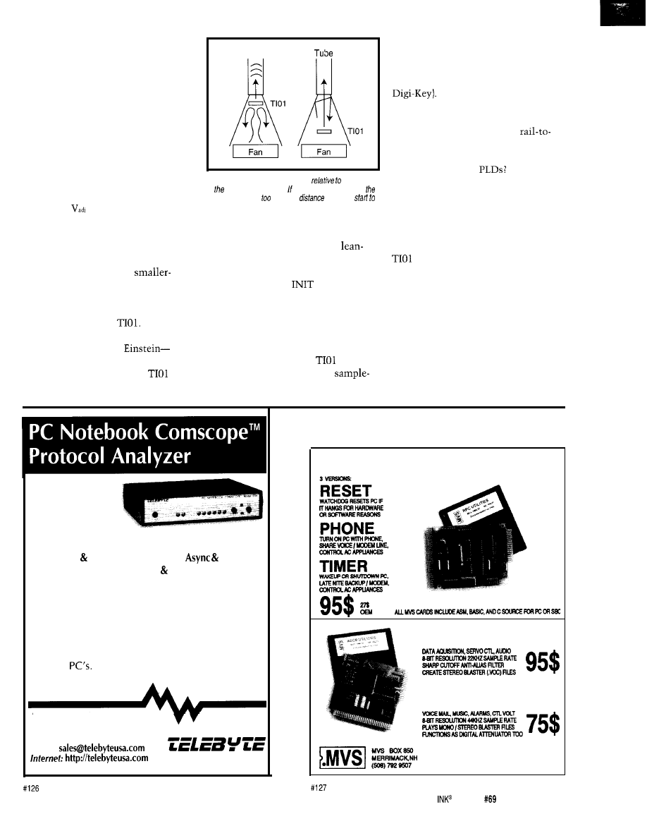
A 12-V regulator input is used for
convenient connection with a power
supply. However, remember that from
the regulator’s point of view, the mini-
mum output is about 1 V. Thus, at
low-speed settings, the regulator sees a
10-V (or more) voltage drop and has to
dissipate a few watts. Originally, a
smaller regulator that looked like it
might make it on paper was tried.
However, even with a heatsink, it
got quite hot and would even go into
thermal shutdown if the fan was left
idling (i.e.,
= 0 V) for a long time.
By contrast, the much beefier LM350
barely gets warm and probably doesn’t
even need a heatsink. Alternatively, a
lower input voltage (say 9 V instead of
12 V) might resurrect the
regulator option.
With success returning the fan to
its analog roots, the same strategy was
contemplated for the
After all,
what’s really being measured is time,
which-though I’m no
seems rather analog to me.
Knowing more about the
than
the AL220, I tried to come up with a
Tube
Figure 4-Transducer positioning
the bottom
of tube is quite critical. it’s too close, it
chokes
airflow, but if if’s far, false
readings
occur.
way
to give the AL220 exactly what it
wants (i.e., O-5 V). The classic
and-mean way to convert time to volt-
age uses an RC that starts charging on
the leading edge of
and is sam-
pled on receipt of echo.
However, at this point, I didn’t
want to impose any timing or synchro-
nization burden on the AL220, fearing
I would regret it later. What’s needed
is a way to decouple the
and
AL220 timing (i.e., provide a
and-hold capability).
The seemingly minor decision
quickly led to a very slippery slope. It
turns out S&H amps are rather arcane
items, with prices to match ($3-6 at
I may as well just use a
counter and a DAC.
For that matter, how about a PIC
processor? I could exploit its
rail outputs and a resistor network
DAC. Gee! What about one of those
newfangled analog
Come to
think of it, why not just use another
AL220 in a fuzzy multiprocessing
configuration?
Talk about tail wagging the dog. I
could see myself spending a lot more
time and transistors just to get the
and AL220 talking than in getting
them to do something useful.
I
finally recognized I’d been avoid-
ing (perhaps, denying) the inevitable.
Clearly, the optimal interface relies on
extensive insight into the detailed
operation of the AL220.
Staring the pile of chip and tool
documentation down, I knew what
had to be done. Yes, it’s a messy job,
but somebody’s got to do it.
l
l
l
l
l
l
l
l
l
l
Menu Driven
Time Stamping
Small-Portable
Travel Case
Built-in Bert Tester
Works with all PC’s Via Serial Port
Monitors Emulates X.25, HDLC,
Bisync
Split Screen Decode of X.25 SDLC
State Machine Programming
Applications Interface Programmable
The Model 904 PC Notebook
Comscope is the latest
addition to Telebyte’s line of powerful and flexible
PC based protocol analyzers. The Model 904 is a
high performance data line monitor, bit error rate
tester and emulator in a small configuration that sup-
ports all
The combination of the 904 and PC
produces a powerful protocol analyzer.
Phone:
l-800-835-3298
(516) 423-3232
Fax:
(516) 385-8184
e-mail:
TECHNOLOGY, INC.
270 Pulaski Road Greenlawn. New York
11740
REMOTE POWER CARD!
8
CHAN ADC
2 CHAN DAC
5 YEAR LIMITED WARRANTY
F R E E S H I P P I N G I N U S A
Circuit Cellar
Issue
April 1996
93
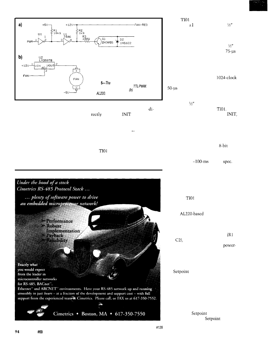
7 4 0 6
F A N - B L K
GND
Figure
original fan module (a) presumed a
digital controller by accepting a
contrast, an analog controller is a better fit with
the
And, it ain’t me, I thought. Picking
u p t h e p h o n e , I e x p l a i n e d m y d i l e m m a
to the experts at Adaptive Logic. Could
they help me finesse the interface a
bit? Needless to say, I gladly accepted
their offer of assistance.
Having successfully delegated all
the hard work to others, the interface
answers suddenly came to me. Yes, I
see now that the only acceptable solu-
tion is to make the AL220 deal with
a n d E C H O ) .
Of course, it’s true that some intri-
cate “ruleware” and clever hardware
t r i c k s m a y b e n e e d e d . .
TIME OUT
To start to get a feel for the AL220
and
interface, let’s take a quick
look at some of the basic timing and
accuracy considerations.
The
specs typical absolute
accuracy of
%,
which is about
given the length (36”) of the tube.
Sound takes about 0.9 ms to travel a
foot, which is doubled to determine
the echo delay. Thus, detecting a
change in ball position requires
echo resolution.
Remember from
INK 67
how the
AL220 runs in kind of a batch mode.
All the inputs are sampled, rules eval-
uated, and outputs set in a
chunk. Thus, the AL220 has roughly
timing resolution running at top
(20 MHz) speed. Quite fortuitously, it
looks like the AL220 is speedy enough
to resolve a
difference and fully
exploit the accuracy of the
So,
just have the AL220 drive
sample ECHO, evaluate the rules, and
drive the fan all at once. It sounds
good, except there’s a small problem.
The speed needed for good resolution
(i.e., -50 us) also means the maximum
loop delay, using the AL220
vari-
ables, is only about 12 ms. This rate is
much too fast, notably show stopped
by the TIOl’s
cycling
The folks at Adaptive were clever
enough to bring the RC delay idea off
the bench for another go. In this case,
the AL220 loops an output back to an
input via an RC to establish a leisurely
overall machine cycle time without
giving up
resolution.
Putting it all together, Figure 6 and
Photo 2 show the refreshingly mini-
malist
PID-Pong machine
controller. Besides the previously dis-
cussed LM350 fan controller (with an
added pot to limit maximum fan out-
put) and cycle time RC network
and
there’s little more to the hard-
ware than the usual clock and
up-reset circuits.
One input is dedicated to a Manual/
Auto switch. In Manual mode, the
AL220 simply copies the input voltage
on
to the Fan output with no
regard for the actual ball position (i.e.,
open loop). This option is useful for
calibrating and testing the machine
and also trying to control the ball
yourself to see how hard it is.
In Auto mode, the AL220 monitors
and regulates the position of the ball
based on the
input. Changing
the voltage input on
exercises
Issue
April 1996
Circuit Cellar INK@
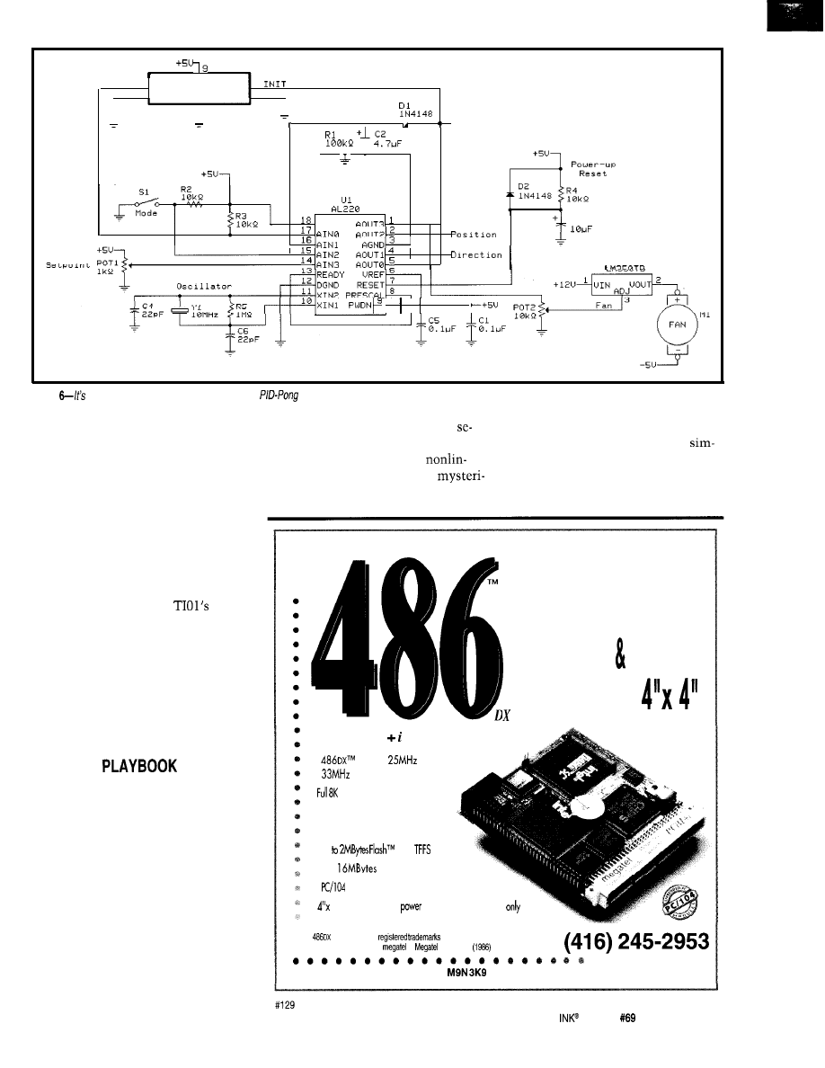
ECHO 7
S o n a r
S e n s o r
4
BLNK 2
8 B I N H
1
P R R T i m e r
M a n u a l / A u t o
UDD
-TOUT
1
c 3
F a n C o n t r o l
u 2
Figure
rather snug, but the AL220 proves up to the
challenge.
the step response of the controller and
machine.
Notice the Direction and Position
outputs don’t seem to go anywhere.
This means these are being used as
buried outputs (i.e., they’re fed back
internally). However, the signals are
available on the pins providing a useful
debug and instrumentation aid.
I think all must agree the design is
quite compelling. Despite being co-
erced into talking on the
terms
(i.e., digital), the AL220 certainly ap-
pears to hold its own against any mi-
cro in terms of chip count and system
cost.
Final judgment on whether the
AL220 deserves a spot in the PID-Pong
hall of fame depends on how well it
plays the game.
PID-PONG
The simplest drill is just to move
the ball to a position and hold it there.
This move is rather easy-even a hu-
man can do it-especially with noth-
ing said about the speed or accuracy of
the movement. Needless to say, this
minimal level of control must be mas-
tered before moving on to advanced
play.
To move the ball back and forth
between setpoints ups the ante. It
sounds easy, but a few attempts at
manual control illustrate just how
tough it is. The machine exhibits
However, even this challenge is
vere lag (on the order of a second) and
manageable by humans (or a real
also an intriguing variety of
ple controller), once you know the
earities, including gravity and
trick. The loophole is that nothing is
ous aerodynamic influences.
said about speed and accuracy. The
l
W O R L D ’ S S M A L L E S T
l
l
l
Embedded PC with
Hooting Point,
Ethernet Super
VGA Only
The
PC/II
includes:
.
CPU at
or
clock frequency
. Cache with Floating Point
. Ethernet local Area Network
. Local Bus Super VGA Video/LCD
. Up
with
. 4 or
User DRAM
l
or
ISA Bus
compatible
option (wih adapter)
. 4” Format; 6 watts
consumption at t5 volt
and Flash are
of Intel Corp.
as are PC, AT of IBM,
of
Computer
Corp.
125
Wendell Ave.
l
Weston, Ont.
l
l
Fax: (416) 245-6505
megatel”
Circuit Cellar
Issue
April 1996
9 5
ENHANCED SOLID STATE
DRIVE
$144”
4M Total, Either Drive Bootable
Card 2 Disk Emulator
Flash System Software Included
FLASH SRAM, Customs too
486 SLAVE PC
CALL
Add up to 4 Boards to One Host PC
Fast Data Transfer and
PC-l 04 Port, IDE Floppy Control
Independent Processors on One Bus
No Special Compilers Needed
TURBO XT
w/FLASH DISK
$266”
To 2 FLASH Drives, 1 M Total
DRAM to 2M
FLASH On-Board
CMOS Surface Mount,
2
Par, Watchdog Timer
Ail Tempustech
products are
PC Bus Compatible.
Made in the
U.S.A., 30 Day Money Back Guarantee
1, Qty
breaks start at 5 pieces.
TEMPUSTECH, INC.
634-0701
Fax for
fast response!
295 Airport
Naples, FL
Photo l--The latest and greatest
version of
machine
a nicer than the original (and
doesn’t use any tape).
generic strategy (whether
human or electronic) is
simply to govern the fan
power high and low limits
to a range that barely lifts
or drops the ball.
The control strategy
then devolves to a simple
bang-bang [i.e., on/off)
algorithm similar to:
IF POSITION <
THEN
FAN=ON
IF POSITION >
THEN
FAN=OFF
It’s only by adding
speed and accuracy re-
quirements that the ma-
chine starts to challenge a
controller and humble a
human operator. For in-
stance, try the following
challenge:
Move the ball between
18"
and 30”
setpoints as fast as possible for
1
min-
ute, achieving stability within
for
at least 3 seconds at each setpoint.
The score equals the number of moves
completed.
My experience is that most mortals
won’t be able to do it at all, while an
on/off controller might hit
l-2
times
as it’s limited by sluggish rise and fall
times. By contrast, an optimal control-
ler, able to move the ball quickly,
could achieve perhaps
moves a
minute.
Even this tougher test, like any
benchmark, is arguably too simple and
prone to manipulation and hijinks.
The problem is the fixed high- and
low-
pattern. It’s possible to
optimize (i.e., cheat) by tweaking gain
factors and fan limits based on know-
ing the setpoints a priori.
A more realistic test could substi-
tute a random or other interesting
pattern of setpoints for the fixed se-
quence of the previous test. The pat-
tern length (i.e., test time) would have
to be long enough to ensure statistical
validity.
An interesting embellishment
might explore the subject of adaptive
control. For instance, the
pattern could be repeated times with
the controller allowed to tune itself
between trials. Comparing the score
after trials to that of the first would
(hopefully) show the
due to
learning.
But wait, it gets even better. We
haven’t even contemplated the inter-
esting subject of disturbances yet.
Disturbances are what make
world control problems challenging, a
reality the PID-Pong machine itself
teaches. Nothing like admiring your
finely (and time-consumingly) tuned
96
Issue
April 1996
Circuit Cellar INK@
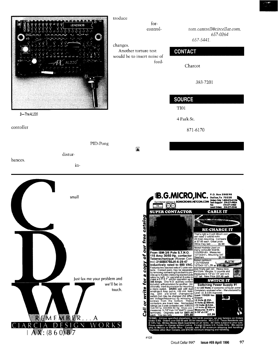
Photo
controller board requires minimal external support
components.
volleying back and forth,
only to have the ball land in your lap
when the air conditioning kicks on.
racing around, now is not
the time to define any
hard-and-fast rules for the
PID-Pong game except
one-have fun and learn something.
That’s just what we’ll do next time
when the AL220 finally takes on the
an offset. It’s not
marketing in Silicon Valley for more
uncommon to see a
than ten years. He may be reached by
merly well-tuned
E-mail at
ler struggle or even fail to
by telephone at (510)
or by
adapt to relatively minor
fax at (510)
various sorts into the
back or control loop. What
the heck, why not goof up
both loops and see how
well your controller might
work across a satellite
link.
Adaptive Logic, Inc.
800
Ave., Ste. 112
San Jose, CA 95131
(408) 383-7200
Fax: (408)
http://www.adaptivelogic.com/
With all these ideas
Ultrasonic Transducer
Micromint, Inc.
Vernon, CT 06066
(860)
Fax: (860) 872-2204
So, once you’ve got a controller
you think passes the previous tests
well, try introducing some
For instance, lay a pencil or
ruler across the top of the tube to
machine.
Let the games begin!
Tom Cantrell has been working on
chip, board, and systems design and
.
434 Very Useful
435 Moderately Useful
436 Not Useful
Does your Big-Company marketing
department come up with more ideas
than the engineering department can
cope with? Are you a
company that can’t afford
a full-time engineering staff for once-in-a-while designs?
Steve Ciarcia and the Ciarcia Design Works
1
staff may have the solution. We have a
team of accomplished programmers
and engineers ready to design
products or solve tricky engineering
problems.
Whether you need an on-line
solution for a unique problem,
a product for a startup venture,
or just experienced consulting,
the Ciarcia Design Works is
ready to work with you.
F
l - 8 9 8 6
The Circuit Cellar BBS
bps
24 hours/7 days a week
(860)
incoming lines
Internet E-mail:
first
discussion
month, we look at a topic familiar to many,
but a mystery to others: Gray codes. Why are they applied and how
are they generated? Read on to find
In the other thread, we compare the use of shunts Ha//-effect
devices for measuring high currents. It’s anything but cut and
Gray code
Msg#: 4172
From: Dave Ewen To: All Users
Anyone spend much time fooling with Gray code? I’m
wondering what the simplest logic is for generating it. I’d
like to fit it in a high-speed PAL and run it like a counter.
Msg#: 4308
From: Pellervo Kaskinen To: Dave Ewen
The following presentation is picked pretty much di-
rectly out of Hamming: Numerical Methods for Scientists
and Engineers,
second edition, ISBN o-07-02887-2.
Building Gray code recursively
l-bit 0
1
00
i.e., 0 1st term of l-bit
01
0 & 2nd term
11
1 2nd term
10
1 1st term
3-bit
000
i.e., 0 1st term of 2-bit
001
0 2nd term
011
0 3rd term
010
0 4th term
110
1 4th term
111
1 3rd term
101
1 2nd term
100
1 1st term
Hamming gives the example to 4-bit level, but believe
the process is clear enough from the description at the right
of each term, with just up to 3-bit level. The 4-bit level of
course contains 16 terms, eight of which are obtained by
padding with a leading 0 and the new eight by padding with
a 1 and taking the terms in reverse order as indicated
above.
98
Issue April 1996
Circuit Cellar
There are other possible Gray codes, but because the rule
of obtaining this particular one is so simple, it has become
to be known as the Gray code.
I hope this covers your needs.
Msg#: 4316
From: Dave Ewen To: Pellervo Kaskinen
Thanks. Doesn’t look like something that can be done in
a PAL too easily, though. I received a suggestion from a
friend that I split it up into nybble-wide Gray-code genera-
tors-each with its own count enable-and then be a little
tricky with the enables to step them only one at a time.
Msg#: 4353
From: Rufus Smith To: Dave Ewen
For lurkers (and participants) out there who may be won-
dering what Gray code is and why it’s useful, file this away
under interesting tidbits.
The beauty and usefulness of Gray code is that only one
bit changes at a time between successive values. This is
extremely important in the world of position encoder de-
vices which detect the position of a mechanism linearly or
rotationally.
The significance is in the transition between values
where a bit change (edge) could be read as either on or off. In
straight binary code, for example, going from 3 to 4 is a
single step, but all three bits are in transition: 011 to 100.
This means that your encoding pickup is on three edges,
each of which could pick up either 1 or 0, potentially read-
ing any value from 000 to 111.
C h a n g e d B i t s
Binary Changed Bits
000
000
001
0
001
0
010
011
1
011
0
010
0
100
110
2
101
0
111
0
110
101
1
111
0
100
0
rollover to 000
000
2
Gray Code, having only one bit in transition at any edge,
always gives a correct reading within one significant bit.
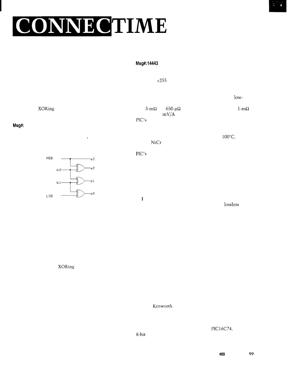
Incidentally, anyone who has worked with quadrature or
incremental encoding has been working with 2-bit Gray
code.
There are several puzzles (the hand-held ring/string/rod
manipulation puzzles) that are solved through the use of
Gray code.
Also the infamous Towers of Hanoi puzzle is also an
example of Gray code at work. The size of the disk to move
is the bit that changes.
I think there is a conversion routine which involves
successively
adjacent bits low to high or high to
low, but I don’t recall it.
4360
From: James Meyer To: Dave Ewen
Here’s a binary-to-Gray converter..
b i n a r y
b 3
G r a y
b O
Note that you will still have to worry about glitches on
the Gray code side because the binary-side bits change more
than one at a time with some counts. A D-type flip-flop
latch per bit with a gate derived from the count input fixes
that, though.
Do your counting in binary and convert that to Gray
code. I’ll bet you’ll be able to fit that into a PAL or two.
Msg#: 4455
From: Dave Ewen To: James Meyer
Hey thanks! Simple
of adjacent binary bits
seems to work fine! That’s something I didn’t know. Where
did you run into that?
Msg#: 4467
From: James Meyer To: Dave Ewen
At the risk of exposing myself as *not
l
all-powerful and
all-knowing, I must admit that I pull a lot of excellent stuff
out of The Art of Electronics by Horowitz and Hill. The
first edition has a catalog number of ISBN O-521-23151-5.
There’s a newer second edition out now (ISBN 0-521-37095-
7).
If I could only have one book, it would have to be The
Art. You
should not rest until you have found a copy.
Hall effect vs. Shunt
From: Mike Mager To: All Users
I want to measure current-in an automotive applica-
tion-up to
A with 1-A resolution. I have tentatively
chosen Hall-effect transduction over resistive-shunt meth-
ods for the following reasons:
To keep the voltage drop low at high current, a
resistance shunt is necessary (no problem, Stuart-Warner
uses
and
units, and possibly lower). A
shunt gives 1
and would require gain to drive the
ADC, a higher-resolution lower-reference-voltage
ADC, or something like that (true?).
A copper or aluminum shunt has a temperature coeffi-
cient of resistance of approximately 40% in
al-
though
or constantan are better.
To use a shunt, with the shunt in the ground return, the
lower reference (Vss) would be connected to the low
end of the shunt, and to accurately read several shunts
would require make-before-break switching of the system’s
Vss from shunt to shunt. With the shunt in the high side,
I’d need an op-amp with a positive supply above the sys-
tem’s battery voltage (true?). The shunt idea seems imprac-
tical here.
So, then, the Hall-effect approach..
need to sense several points, in each of several vehicles,
and a Hall-effect device would seem to allow
and
floating sensing, needing only a small amount of gain to
drive an ADC.
Does anybody have suggestions about a source of sensor
units!
Does anybody have comments on building sensor units
using a slit-core and analog Hall-effect devices? I saw some-
thing in an old Popular Electronics (I think it was, tempo-
rarily lost now) using microswitch Hall-effect devices, a slit
core, and calibrated gain.
Does anybody know about a dedicated absolute-value
circuit, or do I need to use an active full-wave rectifier with
a comparator for sign?
Relative to this project are tow trucks with electricly
driven hydraulic systems. They use about 225 A at the
relief valve setting, BCI group SD batteries, 1300 CCA (400
minutes reserve), and Leece-Neville 2800JB 160-A alterna-
tors. The alternators are typically used on Cummins en-
gines in
trucks, fire trucks, school buses with
wheelchair lifts, and similar applications. I overhauled
them and adapted them to the gasoline engines in the tow
trucks.
(Oh, yeah. This is to be used with a
having an
ADC, 5-V referenced.)
Thanks!
Circuit Cellar INK@’
Issue
April 1996
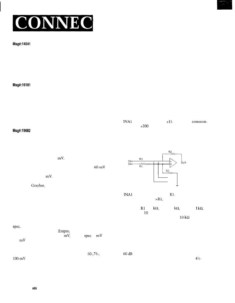
TIME
From: Lyndon Walker To: Mike Mager
A t r i p t h r o u g h t h e
y i e l d s
lute-value circuits. But looking in Analog Devices’
S
p
e
c
i
a
l
the AD737 RMS-to-DC converter
suggests that it can be used as an absolute-value output
f r o m a D C i n p u t .
extra power supply idea should not be considered. In fact,
a n i s o l a t i o n p o w e r s u p p l y f r o m B u r r - B r o w n , w i t h a p r i c e t a g
a r o u n d $ 1 0 i n s m a l l q u a n t i t i e s , w o u l d b e r e a s o n a b l y c o m -
Thanks for taking time to find an absolute-value circuit!
I h a d n ’ t t h o u g h t o f t h e R M S c o n v e r t e r t h a t w a y , b u t , y e a h ,
is
what it does. Sadly, it doesn’t have the sign output,
s o i t ’ s j u s t a n e x p e n s i v e r e c t i f i e r i n m y c a s e . I f o u n d a l l
s o r t s o f s t u f f t h a t w a s a l m o s t , b u t n o t q u i t e , w h a t I w a n t e d
i n t h e M a x i m b o o k s . I f y o u ’ r e d e s i g n i n g a p o r t a b l e c o m -
You could use an isolation amplifier. Those amplifiers
h a v e t h e i r o w n p o w e r i s o l a t i o n a n d c o u p l e t h e s i g n a l
using optocouplers. You could build your own for 30-100
b u c k s f r o m c o m p o n e n t s a v a i l a b l e f r o m B u r r - B r o w n o r A n a -
linear device based on a Siemens chip (I forget the exact
name, something like ILC-300).
Another option would be the signal conditioning mod-
u l e s i n t h e 3 B a n d 5 B s e r i e s f r o m A n a l o g D e v i c e s .
From: Pellervo Kaskinen To: Mike Mager
There are several possibilities, some even beyond what
you have mentioned so far. But, I’ll start with the items you
presented.
And then, to show the low-cost option: Use an extended
common-mode differential amplifier. Burr-Brown sells their
model
17 that operates from
V and has a
mode range up to
V, while providing a unity gain for
the differential input to the single-ended output. To provide
a good enough common-mode rejection, they laser trim the
resistors inside, but I use plain 1% resistors in my designs
with adequate results. Here is the basic circuit:
A commercial shunt is likely to be defined at a fixed,
full-scale voltage level of 50
whatever its current rat-
ing. This is due to the fact that any analog meters pretty
much had to be standardized. Actually, in Europe a
standard emerged, while the U.S. trend setters [Weston, GE,
and others) chose 50
Anyway, if you go to an electric supply house, such as
GE supply,
or several others that are more local-
ized, you can buy almost any shunt you want, with some
more popular ones off the shelf. A full scale of 255 A,
though, is a far call still today. More likely, you would find
200-A and 300-A units. But no problem with your 225 A, in
most cases: Just use a 200-A unit. They are very robust and
the 25 extra amperes won’t harm them any time soon. Of
course, you have to provide adequate ventilation around the
shunt or the accuracy would fall out of the usual 0.25%
R 3
,
R3
The
17 has essentially R2 =
But if you want to
get gain, you can make R2
with R3 affecting only the
common-mode range.
Some companies, such as
make shunts to your
specifications. Instead of the 50
you can
75
or
100
if they better fit your needs. The higher voltages
naturally mean higher power dissipation. That again tends
to translate into larger physical size. At the suggested 200-A
level, the power is 10 W, 15 W, or 20 W for the
and
units, respectively. At your 225 A, it would be
about 20% more.
Say, you have = 10
R2 = 100
and R3 =
to produce a gain of and a common-mode range of at
least 100 V. Maybe I need to state that the
input
resistors might not be too happy about the 100 V, unless
you use at least 1-W resistors. But, the actual resistance
values can be scaled by any factor to accommodate the
power dissipation requirements.
To avoid a need for trimmer potentiometers, the resis-
tors should be as accurately matched as you can make
them. The easy way would be to pick 0.1% resistors that
offer a
common-mode attenuation off the box. Other-
wise, get 1% resistors and find matched pairs with a
digit DVM or other resistance meter.
Contrary to your belief, no extra power supply above the
You can also use a bridge technique, where you at first
positive rail would be necessary in several schemes, even
find four resistors that produce a balance no matter what
when the shunt is on the high side. This does not mean the
order the four elements are combined. Then use two of
100
Issue
April 1996
Circuit Cellar INK@
these resistors as a basis for a permanent bridge to measure
any other resistors. Put the other two away for any future
replacement need.
Then to the Hall-effect front..
While you were concerned about the thermal stability of
copper as a shunt material, the Hall-effect devices are
worse! They really make quite sensitive temperature-mea-
surement devices, with a secondary use for magnetic-field
detection. :-)
The way out of that dilemma, of course, can be using
two of them in a half bridge. One would be mounted so the
magnetic field does not affect it, while the second one
would be in the gap of the core. That corrects the bulk of
the sensitivity shift by temperature. It still leaves a major
nonlinearity. The way out of both the temperature and the
linearity problems is to make a feedback arrangement.
A Hall-effect current-measuring device with feedback is
based on the idea that the Hall-effect sensor is operated at
zero flux. Any deviation from zero is amplified and fed to a
secondary winding on the same core. If the primary winding
is 1 turn and the secondary winding is 5000 turns, then a
250-A primary flux would be fully canceled by 50
at the
secondary. Then, all you need is to measure the 50
A
100-G resistor would generate 5 V for your PIC ADC.
You need a power op-amp to force the
current,
but it is regularly done. To my understanding, the first
source for such devices was LEM. Now also Honeywell and
F.W. Bell offer feedback-based current transducers.
Now, a few words about some other possibilities. You
can measure DC currents with a device called a
tor.
It is based on the DC primary shifting the two satura-
tion points of two
cores that are driven by AC
excitation. Again, the DC primary is a single turn, while
the secondary consists of thousands of turns on each of the
two cores. The secondaries are connected in series, but in
opposite directions.
As long as there is no DC, they offer a high impedance to
the AC. But when the saturation points change, the AC
excitation starts producing current. In fact, it is pretty
straight proportional to the DC current.
I have used them in the past, but now find them cumber-
some and only applicable when the currents get to the
range. (Imagine the power dissipation of a
shunt at 100
The BCC52 controller continues to be
Micromint’s best selling single-board com-
puter. Its cost-effective architecture needs
only a power supply and terminal to become
a complete development system or
board solution in an end-use system. The
BCC52 is programmable in BASIC-52, (a
fast, full floating point interpreted BASIC), or
assembly language.
The BCC52 contains five RAM/ROM
sockets, an
EPROM
programmer, three” b-bit parallel ports, an
auto-baud rate detect serial console port, a serial printer port, and much more.
PROCESSOR
CMOS processor w/BASIC-52
. Console
detect
.
printer RS-232
interrupts
. Three
parallel ports
more!
EXPANDABLE!
12 BCC
boards
RAM/ROM, expandable
on-board memory sockets
EPROM
Product and Pa
n
Engineering Stock
N E W L O W E R P R I C E S !
B C C 5 2
Controller board
BASIC-52 and RAM
$179.00
temperature
$ 2 0 4 . 0 0
BCC 5
Low-power CMOS, expanded BCC52
RAM
$ 1 9 9 . 0 0
CALL FOR OEM PRICING
INC.
Vernon, CT06066
Europe
Canada: (514)
Inquiries
Circuit Cellar INK@
Issue
April 1996
101
Sometimes you may not need very complicated DC mea-
suring at all. If you can put a standard AC current trans-
former on the AC leg before the rectifier [in the alternator),
you get a good representation of the DC current. Actually, if
you put in a current transformer on all three AC legs to the
rectifier and then put a three-phase bridge rectifier to the
output of the three current transformers, you get an exact
representation of the DC. It is scaled by the transformer
turns ratio. Connecting the necessary (compulsory) load
resistance to the DC leg of the secondary rectifier elimi-
nates the diode drop effect of the secondary rectifier.
You can scale the output voltage by selecting the load
resistance value. But you have to make sure the transform-
ers are not saturated by the imposed load voltage. Also,
many alternators use a three-phase half bridge as the main
rectifier. Such an arrangement is not well suited for the
current transformer method described above.
This list is by no means exhaustive, but I hope you find
it thought provoking. After all, even though your descrip-
tion of the application needs was quite thorough, there still
may be details that I do not know. So the final choices re-
main yours.
One of Micromint’s hottest-selling products for the past five years
has been the
stackable controller. It has been a leading
formance choice among our customers. With our new RTC320 board, we
have expanded the value of that relationship even more.
Occupying the same small
RTC footprint and using S-V-only
power, the RTC320 uses the new Dallas Semiconductor
which is
8031 code compatible and 3-5 times faster. At 33 MHz, the
is an
controller! Along with the new powerful processor, the RTC320 board
accommodates up to 192 KB of memory, two serial ports (RS-232 and
24 bits of
parallel l/O, and a
ADC. The
puts
some real firepower under the abundant variety of RTC I/O expansion boards.
CALL l-800-635-3355 TO
4
102
April1996
Circuit Cellar INK@
From: Mike Mager To: Pellervo Kaskinen
Part of my requirement was for the transduction to be
low enough priced that several points on each of several
tow trucks could be measured. These would be battery
current, alternator current (positive only), and hoist motor
current (negative only).
I would like to get
to
accuracy, in a practical
sense, not in a laboratory sense. I’m with you on the shunts,
as far as power dissipation, voltage drop, and so on, and the
compromise would be between low voltage drop and low
required gain. I’m concerned about noise with a high gain.
The feedback method of linearizing a Hall-effect device
seems interesting! I could build them, I think. Have you
any references on the practicalities?
From: Pellervo Kaskinen To: Mike Mager
am not sure, but I might find some useful info from
LEM documents. I’ll take a look. On the other hand, the
F.W. Bell parts are quite low in price.
We invite you to call the Circuit Cellar BBS and exchange
messages and files with other Circuit Cellar readers. It is
available 24 hours a day and may be reached at (860)
1988. Set your modem for 8 data bits, stop bit, no parity,
and 300,
9600, or
bps.
Software for the articles in this and past issues of
Circuit Cellar INK
may be downloaded from the
Circuit Cellar BBS free of charge. It is also available on
the Internet at
Web
users should point their browser at
For those with just E-mail access, send
a message to
to find out how to
request files through E-mail.
For those unable to download files, the software is
also available on one 360 KB IBM PC-format disk for
only $12. To order Software on Disk, send check or
money order to: Circuit Cellar INK, Software On
Disk, P.O. Box 772, Vernon, CT 06066, or use your
Visa or Mastercard and call (860) 8752199. Be sure to
specify the issue number of each disk you order.
Please add $3 for shipping outside the U.S.
.
437
Very Useful
438 Moderately Useful
439 Not Useful

INTERRUPT
Not Just Ferengi Values
t
here are two ways to learn things in life: trial and error (experience) or by what someone tells you
(education). Your behavior is also affected by what you’ve learned. If you grew up always thinking that
wearing the color green means you’re Irish, then as a Russian or Greek, you’d probably avoid green. Similarly, if
you grew up on the impoverished side of town and never saw an upwardly mobile role model, you might resign yourself to a life with
few options.
For many young people today, film and broadcast media have become primary education and information sources. Unfortu-
nately, in my opinion, these media people view their influence and effect with about the same responsibility as those selling a box of
Tide. However, because this influence is real, it is important to challenge these obvious biases.
One area where I believe film and broadcast media are biased is in their negative attitude toward business. Cloaked in dramas
or comedies, businesses are often equated with dark escapades, indiscretion, and greed. Only when observed in historical perspec-
tive are they correctly viewed as having contributed to the potency and prestige of the United States’ industrial power. Other than that,
business is a four-letter word.
I’m not disputing that some corporations appear to treat employees as cannon fodder. I’m merely criticizing the media bias
which results from their obsession with these “business detractors.” Such an attitude shouldn’t be applied to all situations involving a
business entity.
The Ferengi value system offers definitive rules to deal with the best and worst aspects of capitalism. It seemed kind of ironic
that a recent episode of
Trek: Deep Space Nine would, while presenting business in a detrimental light, offer as its primary
malevolence, that which perpetuates its positive existence.
In a dispute over working conditions in Quark’s bar, the issue of collective action was presented as a suggested maneuver.
Of course, the Ferengi employees were initially appalled at the concept. Under their value system, the control Quark was dispensing
they would also seek to command if they were in his place. Undermining the process that enables Quark to dominate merely
undermines their potential for ever achieving equivalent authority.
In a society which has only business to support its continued existence, we delude ourselves to think otherwise. Government
doesn’t make money, it only spends money. It is the positive relationship between people working for businesses that produce
products and the resulting wages they spend buying products that creates money in an economy.
The realization is that, unless you are supported by government, you are sustained by business. The engineering consulting you
do is a business product; the embedded controller you’re hoping to market is a business product; to feed your family, the job you have
is in a business.
I apologize if this sounds like preaching. Perhaps it’s people like me who have started businesses who feel the greatest need to
protect a system that offers such opportunity. Describing something always in negative terms is hardly incentive for others to join the
cause. It’s time to balance the equation with a little experience...Flame off.
112 Issue April
1996
INK@
Wyszukiwarka
Podobne podstrony:
circuit cellar1996 04
circuit cellar1991 04,05
circuit cellar2001 04
circuit cellar2002 04
circuit cellar1995 04
circuit cellar1994 04
circuit cellar2004 04
circuit cellar1992 04,05
circuit cellar2000 04
circuit cellar1990 04,05
circuit cellar2003 04
circuit cellar1997 04
circuit cellar1996 04
circuit cellar1991 04,05
circuit cellar2001 04
circuit cellar1992 04,05
circuit cellar1995 04
circuit cellar1997 04
więcej podobnych podstron