
Layout Guidelines for
Switching Power Supplies
Introduction
When designing a high frequency switching regulated power
supply, layout is very important. Using a good layout can
solve many problems associated with these types of sup-
plies. The problems due to a bad layout are often seen at
high current levels and are usually more obvious at large in-
put to output voltage differentials. Some of the main prob-
lems are loss of regulation at high output current and/or large
input to output voltage differentials, excessive noise on the
output and switch waveforms, and instability. Using the
simple guidelines that follow will help minimize these prob-
lems.
Inductor
Always try to use a low EMI inductor with a ferrite type closed
core. Some examples would be toroid and encased E core
inductors. Open core can be used if they have low EMI char-
acteristics and are located a bit more away from the low
power traces and components. It would also be a good idea
to make the poles perpendicular to the PCB as well if using
an open core. Stick cores usually emit the most unwanted
noise.
Feedback
Try to run the feedback trace as far from the inductor and
noisy power traces as possible. You would also like the feed-
back trace to be as direct as possible and somewhat thick.
These two sometimes involve a trade-off, but keeping it
away from inductor EMI and other noise sources is the more
critical of the two. It is often a good idea to run the feedback
trace on the side of the PCB opposite of the inductor with a
ground plane separating the two.
Filter Capacitors
When using a low value ceramic input filter capacitor, it
should be located as close to the V
IN
pin of the IC as pos-
sible. This will eliminate as much trace inductance effects as
possible and give the internal IC rail a cleaner voltage sup-
ply. Some designs require the use of a feed-forward capaci-
tor connected from the output to the feedback pin as well,
usually for stability reasons. In this case it should also be po-
sitioned as close to the IC as possible. Using surface mount
capacitors also reduces lead length and lessens the chance
of noise coupling into the effective antenna created by
through-hole components.
Compensation
If external compensation components are needed for stabil-
ity, they should also be placed closed to the IC. Surface
mount components are recommended here as well for the
same reasons discussed for the filter capacitors. These
should not be located very close to the inductor as well.
Traces and Ground Plane
Make all of the power (high current) traces as short, direct,
and thick as possible. It is a good practice on a standard
PCB board to make the traces an absolute minimum of 15
mils (0.381mm) per Ampere. The inductor, output capacitors,
and output diode should be as close to each other possible.
This helps reduce the EMI radiated by the power traces due
to the high switching currents through them. This will also re-
duce lead inductance and resistance as well which in turn re-
duces noise spikes, ringing, and resistive losses which pro-
duce voltage errors. The grounds of the IC, input capacitors,
output capacitors, and output diode (if applicable) should be
connected close together directly to a ground plane. It would
also be a good idea to have a ground plane on both sides of
the PCB. This will reduce noise as well by reducing ground
loop errors as well as by absorbing more of the EMI radiated
by the inductor. For multi-layer boards with more than two
layers, a ground plane can be used to separate the power
plane (where the power traces and components are) and the
signal plane (where the feedback and compensation and
components are) for improved performance. On multi-layer
boards the use of vias will be required to connect traces and
different planes. It is good practice to use one standard via
per 200mA of current if the trace will need to conduct a sig-
nificant amount of current from one plane to the other.
Arrange the components so that the switching current loops
curl in the same direction. Due to the way switching regula-
tors operate, there are two power states. One state when the
switch is on and one when the switch is off. During each
state there will be a current loop made by the power compo-
nents that are currently conducting. Place the power compo-
nents so that during each of the two states the current loop
is conducting in the same direction. This prevents magnetic
field reversal caused by the traces between the two
half-cycles and reduces radiated EMI.
Heat Sinking
When using a surface mount power IC or external power
switches, the PCB can often be used as the heatsink. This is
done by simply using the copper area of the PCB to transfer
heat from the device. Refer to the device datasheet for infor-
mation on using the PCB as a heatsink for that particular de-
vice. This can often eliminate the need for an externally at-
tached heatsink.
These guidelines apply for any inductive switching power
supply. These include Step-down (Buck), Step-up (Boost),
Flyback, inverting Buck/Boost, and SEPIC among others.
The guidelines are also useful for linear regulators, which
also use a feedback control scheme, that are used in con-
junction with switching regulators or switched capacitor con-
verters. Some layout pictures are included:
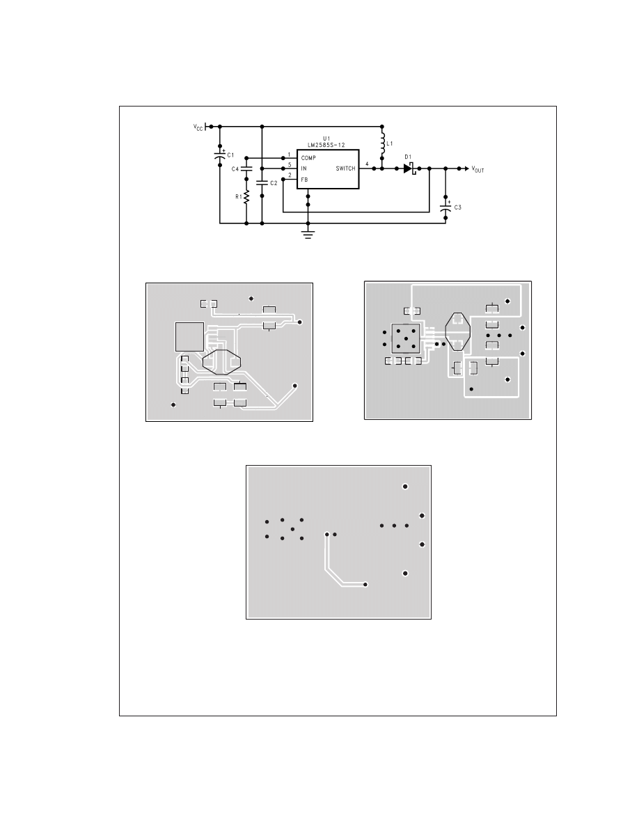
Figure 1 shows
Step-up switching regulator schematic to be used for some
layout examples.
Figure 2 is an example of a bad layout that
violates many of the suggestions given.
Figure 3 and Figure
4 show an example of a good layout that incorporates most
of the suggestion given.
National Semiconductor
Application Note 1149
Clinton Jensen
October 1999
Layout
Guidelines
for
Switching
Power
Supplies
AN-1
149
© 1999 National Semiconductor Corporation
AN101247
www.national.com
AN101247-1
FIGURE 1. Step-up Switching Regulator Schematic
C1
C3
C4
R1
C2
D1
U1
LM2585S-12
VCC
GND
GND
L1
VOUt
1
AN101247-4
FIGURE 2. Bad Layout Example
R1
C4
D1
C3
VOUT
GND
GND
VCC
C1
L1
C2
U1
LM2585S–12
1
AN101247-3
FIGURE 3. Good Layout Example, Top Layer
AN101247-2
FIGURE 4. Good Layout Example, Bottom Layer
AN-1
149
www.national.com
2

Notes
LIFE SUPPORT POLICY
NATIONAL’S PRODUCTS ARE NOT AUTHORIZED FOR USE AS CRITICAL COMPONENTS IN LIFE SUPPORT
DEVICES OR SYSTEMS WITHOUT THE EXPRESS WRITTEN APPROVAL OF THE PRESIDENT AND GENERAL
COUNSEL OF NATIONAL SEMICONDUCTOR CORPORATION. As used herein:
1. Life support devices or systems are devices or
systems which, (a) are intended for surgical implant
into the body, or (b) support or sustain life, and
whose failure to perform when properly used in
accordance with instructions for use provided in the
labeling, can be reasonably expected to result in a
significant injury to the user.
2. A critical component is any component of a life
support device or system whose failure to perform
can be reasonably expected to cause the failure of
the life support device or system, or to affect its
safety or effectiveness.
National Semiconductor
Corporation
Americas
Tel: 1-800-272-9959
Fax: 1-800-737-7018
Email: support@nsc.com
National Semiconductor
Europe
Fax: +49 (0) 1 80-530 85 86
Email: europe.support@nsc.com
Deutsch Tel: +49 (0) 1 80-530 85 85
English
Tel: +49 (0) 1 80-532 78 32
Français Tel: +49 (0) 1 80-532 93 58
Italiano
Tel: +49 (0) 1 80-534 16 80
National Semiconductor
Asia Pacific Customer
Response Group
Tel: 65-2544466
Fax: 65-2504466
Email: sea.support@nsc.com
National Semiconductor
Japan Ltd.
Tel: 81-3-5639-7560
Fax: 81-3-5639-7507
www.national.com
Layout
Guidelines
for
Switching
Power
Supplies
AN-1
149
National does not assume any responsibility for use of any circuitry described, no circuit patent licenses are implied and National reserves the right at any time without notice to change said circuitry and specifications.
Wyszukiwarka
Podobne podstrony:
(Wydruk – ATX Switching Power Supply 13,8 V Proste zmiany w celu zwiększenia napięcia wyjściowego Ja
Adaptive fuzzy control for uninterruptible power supply with three phase PWM inverter
Adaptive fuzzy control for uninterruptible power supply with three phase PWM inverter
Power MOS FET in Switching Power Supply
Switching Power Supply Tutorial
Digital Control Of Switching Power Supply Power Factor Correction Stage
Switching Power Supply 2
SWITCHING POWER SUPPLY DESIGN CONTINUOUS MODE FLYBACK CONVERTER
17V 10A Switch Mode Power Supply (PCB layout) 020054 3
Battery Inverter For Modularly Structured Pv Power Supply Systems
Control and Power Supply for Resistance Spot Welding (RSW)
(ebook electronics) Schematics Power Regulated Power Supply for CB & Ham Radio
SI 8033JD, SI 8050JD, SI 8090JD Surface Mount, Separate Excitation Switching Type Power Supply ICes
A 12kw Switching Mode Power Supply With Free Input Voltage
Power Supply For Oled Driver
DESIGN OF A SWITCHING MODE POWER SUPPLY WITH UPS FEATURES
więcej podobnych podstron