
A High Sensitive Piezoresistive Sensor for Stress
Measurements in Packaged Semiconductor Die
Ahsan Mian, Jeffrey C. Suhling, and Richard C. Jaeger
Abstract----- The authors have developed new two-
dimensional piezoresistive stress sensors that replace
conventional serpentine resistor rosettes. These sensors
are named van der Pauw (VDP) sensors as they are
based upon four-terminal van der Pauw type resistance
measurements. The resistance of such a sensor is size
independent, and hence can be made as small as
lithographically possible to capture stresses in critical
areas on the surface of a packaged semiconductor die. It
was predicted theoretically that the VDP sensor should
exhibit a greater than three times improvement in
sensitivity relative to resistor sensor rosettes. Then the
response of actual VDP structures fabricated on (111)
silicon surface was characterized under uniaxial load
using four-point-bending tests. These experimental
results confirm that the VDP stress sensitivities are more
than three times higher than those of their corresponding
resistor sensor counterparts.
I
.
I
NTRODUCTION
For many years, resistive stress sensors have been used
successfully to measure die stresses in a wide range of
packaging applications [1-2]. However, resistor sensors
possess several drawbacks. Diffused and implanted resistors
have high temperature sensitivity relative to the stress
response, and great care must be exercised to achieve
accurate measurement of stress. Resistors are often designed
with relatively large meandering patterns to increase the
total resistance, but they then suffer from transverse
sensitivity which is difficult to estimate due to the lateral
diffusion that occurs during the fabrication process.
Transverse sensitivity can be minimized by interconnecting
resistor legs with metal links, but these require additional
contacts that further increase the resistor size.
In a paper published recently [3],
the authors have fully
developed the theory for a new piezoresistive stress sensor
termed the van der Pauw (VDP) sensor that is designed to
replace conventional serpentine resistor sensors. The sensor
utilizes the technique of measuring “resistances” based on
the theoretical developments of van der Pauw. When used
as stress sensors, VDP devices have the potential to reduce
some of the error sources in resistor-based sensors. As will
be demonstrated, they offer a greater than thee times
increase in sensitivity compared to that of resistors, and
therefore they also exhibit a corresponding reduction in
A. Mian is with the Dept. of Mechanical and Industrial Eng., Montana
State University, Bozeman, Montana 59717 (
amian@me.montana.edu
)
J. C. Suhling is with the Dept. of Mechanical Eng., Auburn University,
Auburn, Alabama 36849
R. C. Jaeger is with the Dept. of Electrical and Computer Eng., Auburn
University, Auburn, Alabama 36849
sensitivity to thermal errors. The classical VDP structure
itself requires only one square of material plus room for four
contacts. Thus, these sensors have the potential to be made
small enough to capture localized stress variations without
any loss of sensitivity. The VDP characteristics are size
independent and do not have the transverse sensitivity issue.
In contrast, it is the distributed nature of the VDP structure
that leads to the enhanced sensitivity.
In this work, the sensitivity of the VDP sensor is first
predicted theoretically. Then, VDP and resistor sensors
fabricated on (111) silicon surfaces are characterized using
uniaxial stress, and the predicted enhancement of the
sensitivity of the sensors is experimentally demonstrated.
II.
V
DP
S
ENSOR
P
IEZORESISTIVE
T
HEORY
The van der Pauw sensor has four electrical contacts A,
B, C, and D located at the four corners of the sample as
shown in Fig. 1. The “resistance” R
AB,CD
of the sample is the
potential difference V
D
-V
C
between contacts D and C per
unit current through contacts A and B. A similar resistance
R
BC,DA
can be defined in an analogous manner. The
orientation
φ of the sensor indicates the angle between the
1
x
′
- axis and the line connecting points A and B. Also, a
simplified notation is introduced for the resistance of the
oriented VDP sensor:
AB
C
D
CD
AB
I
V
V
R
R
/
)
(
,
−
=
=
φ
(1)
Note that a given VDP structure as shown in Fig. 1 can be
used to measure both
φ
R
and
90
+
φ
R
.
A local coordinate system has also been considered
denoted by the
1
x
′′ -
2
x
′′ axes that are directed along the edges
of the VDP sensor. As developed in [3], the sensor
resistance change equations for such sensors fabricated on
(111) silicon surfaces are given as
′
−
+
′
−
−
′
−
=
∆
−
∆
23
22
1
1
11
2
1
90
90
0
0
)
(
2
4
)
(
)
(
16
.
3
3
2
σ
σ
σ
n
n
B
B
B
B
B
B
R
R
R
R
(2)
[
]
12
2
1
13
2
1
45
45
45
45
)
(
2
)
(
2
4
16
.
3
σ
σ
′
−
+
′
−
=
∆
−
∆
−
−
B
B
B
B
R
R
R
R
(3)
The normalized resistance change is defined by
0
0
/
)
(
/
φ
φ
σ
φ
φ
φ
R
R
R
R
R
−
=
∆
(4)
where
σ
φ
R
is the resistance measured for the stressed VDP,
and
0
φ
R
is the reference resistance measured for the
“unstressed” sensor.
In order to verify the theory, we focus on the uniaxial
stress case where
σ
σ
=
′
11
is applied in
1
x
′
direction, and all
other stress components are assumed to be zero. For this
case, the difference between the normalized resistance
19
1-4244-0374-X/06/$20.00 © 2006 IEEE
Authorized licensed use limited to: Politechnika Slaska. Downloaded on May 29, 2009 at 04:23 from IEEE Xplore. Restrictions apply.
changes for a
φ = 0
o
VDP sensor can be obtained from Eqs.
(2) and (3) as
σ
)
(
16
.
3
2
1
90
90
0
0
B
B
R
R
R
R
−
=
∆
−
∆
(5)
whereas the difference between the normalized resistance
changes for a 0/90
o
pair of resistors calculated in [2] is
σ
)
(
2
1
90
90
0
0
B
B
R
R
R
R
−
=
∆
−
∆
(6)
The responses in Eq. (5) is 3.16 times larger than those
produced by the corresponding resistor rosette fabricated on
the same wafer with the same doping level and result from
the distributed nature of the two-dimensional VDP sensor.
In the next sections, this enhanced sensitivity is verified
experimentally.
φ
1
x
′
2
x
′
A
B
D
C
1
x
′′
2
x
′′
n
Figure 1 - Oriented Rectangular VDP Sensor
(17)
III.
E
XPERIMENTAL
M
EASUREMENTS
For experimental verification, VDP test structures were
fabricated on (111) silicon surfaces using standard
semiconductor processing at Auburn University. As an
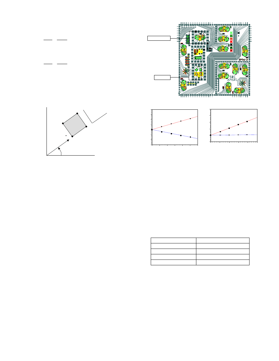
example, Fig. 2 shows the layout of the BMW-2 resistor test
chip, which has been fabricated using (111) silicon wafer.
In this die, a separate VDP test cell was included which
contains two p-type and two n-type VDP sensors. For each
type of doping, one VDP sensor is oriented at
φ = 0
o
(allowing measurement of R
0
and R
90
), and the other is
oriented at
φ = 45
o
(allowing measurement of R
45
and R
-45
).
In the present analysis, only results for the
φ = 0
o
sensors are
discussed, since the 45
o
sensors are designed to measure
shear stress which is not easily applied in a controlled
manner. The test chip also contains the resistor rosette test
site indicated in Fig. 2 as well as process test sites and a
dozen measurement rosettes.
The variation of the resistances of the VDP structures
with applied uniaxial stress has been measured using four-
point bending tests. The silicon wafers containing the test
chips were cut into rectangular strips. Each strip contains a
series of chips, and was loaded in a four-point bending
fixture to apply uniaxial stress. Resistances
0
R and
90
R were
measured for various load conditions and plotted as a
function of the applied stress. Figures 3a shows the typical
plot of normalized resistance change versus applied stress
for p-type sensor. The responses of the sensors to applied
uniaxial stress are highly linear. The difference of the
resistance changes were extracted from the data in Fig. 3a
and are plotted against stress in Fig. 3b.
VDP Cell
Resistor Rosettes
Figure 2 - (111) silicon test chip layout with VDP sensors
Uniaxial Stress (MPa)
0
20
40
60
80
100
120
-0.15
-0.10
-0.05
0.00
0.05
0.10
0.15
0.20
φ = 0
o
φ = 90
o
∆R
0
/R
0
∆R
90
/R
90
Uniaxial Stress (MPa)
0
20
40
60
80
100
120
-0.15
-0.10
-0.05
0.00
0.05
0.10
0.15
0.20
φ = 0
o
φ = 90
o
∆R
0
/R
0
∆R
90
/R
90
∆R
0
/R
0
∆R
90
/R
90
Uniaxial Stress (MPa)
0
20
40
60
80
100
-0.1
0.0
0.1
0.2
0.3
0.4
∆R
0
/R
0
-
∆R
90
/R
90
∆R
0
/R
0
+
∆R
90
/R
90
(a) (b)
Figure 3 - Typical experimental data p-type sensor
Similar tests were performed on several p- and n-type
VDP sensors from the same wafer. The average values of
the sensitivities are summarized in Table 1. Also given in
Table 1 are the stress sensitivities for the analogous 0/90
resistor pairs, which were calculated using Eq. (6). The
stress sensitivity in this case is (B
1
– B
2
) and were measured
from the resistor rosettes. It is apparent form the tabulated
experimental data that the responses of the difference of the
normalized resistance changes to stress are 3.18
(1874.9/590.4) times for larger p-type and 3.32 (-413.9/-
425.4) times larger for n-type sensors than the responses
experienced by the analogous 0
o
/90
o
resistor sensor rosettes.
Sensor Type
Stress Sensitivity (1/TPa)
p-type VDP
+1874.8
n-type VDP
-1413.9
p-type Resistors
+590.4
n-type Resistors
-425.4
Table 1 – Stress Sensitivities for VDP and Resistor Sensors
IV. R
EFERENCES
[1] D. A. Bittle, J. C. Suhling, R. E. Beaty, R. C. Jaeger and
R. W. Johnson, “Piezoresistive Stress Sensors for
Structural Analysis of Electronic Packaging,” Journal of
Electronic Packaging, Vol. 113(3), pp. 203-215, 1991.
[2] J. C. Suhling and R. C. Jaeger, “Silicon piezoresistive
stress sensors and their application in electronic
packaging,” IEEE Sensors Journal, vol. 1, no. 1, pp. 14-
30, June 2001.
[3] A. Mian, J. C. Suhling and R. C. Jaeger, “The van der
Pauw Stress Sensor," IEEE Sensors Journal (in press).
20
1-4244-0374-X/06/$20.00 © 2006 IEEE
Authorized licensed use limited to: Politechnika Slaska. Downloaded on May 29, 2009 at 04:23 from IEEE Xplore. Restrictions apply.
Wyszukiwarka
Podobne podstrony:
Drilling Fluid Yield Stress Measurement Techniques for Improved understanding of critical fluid p
A Technique to Measure Eyelid Pressure using Piezoresistive Sensors
Force Measurements In A Scanning Force Microscope With Piezoresistive Sensors
Measuring the deflection of a micromachined cantilever in cantilever device using a piezoresistive s
A Low Cost Integrated Approach for Balancing an Array of Piezoresistive Sensors
Drilling Fluid Yield Stress Measurement Techniques for Improved understanding of critical fluid p
Design Guide 17 High Strength Bolts A Primer for Structural Engineers
Japanese high school students’ motivation for extensive L2 reading
piezoresistive sensor rosettes
NASA CR 180678 Calculation of Aerodynamic Characteristics at High Angles of Attack for Airplane Conf
2007 A High Protein, High Fiber Diet Designed for Weight Loss Improves
Tai chi for Stress and Relaxation 2
piezoresistive sensors
high level tool High level Tool Targeted for AVR Controllers
4 39 48 New Hot Work Steel for High Temp and High Stress Service Conditions
23 299 318 Optimizing Microstructure for High Toughness Cold Work Steels
Shakespeare Measure for Measure
więcej podobnych podstron