
IEEE TRANSACTIONS ON INDUSTRIAL ELECTRONICS, VOL. 48, NO. 2, APRIL 2001
309
A Simplified Functional Simulation Model for
Three-Phase Voltage-Source Inverter Using
Switching Function Concept
Byoung-Kuk Lee, Student Member, IEEE, and Mehrdad Ehsani, Fellow, IEEE
Abstract—In this paper, a functional simulation model for the
voltage-source inverter (VSI) using the switching function concept
is studied and the actual implementation of the model is proposed
with the help of Matlab Simulink. Also, this concept is extended
to the voltage-doubler-type pulsewidth-modulated (PWM) ac–dc
rectifier and the PWM Ac–dc–ac converter. With the developed
functional model, the simplification of the static power circuits can
be achieved so that the convergence and long run-time problems
can be solved. Also, in the functional model, the design parame-
ters, such as voltage and current ratings of the power semicon-
ductor switches and load current, can be easily calculated. The
general switching function concept is reviewed in brief and the pro-
posed functional models for the VSI, voltage-doubler rectifier, and
PWM ac–dc–ac converter and their implementations using Matlab
Simulink are explained in detail. Also, several informative simula-
tion results verify the validity of the proposed models.
Index Terms—Functional model, pulsewidth-modulation con-
verter, pulsewidth-modulation rectifier, switching function, voltage-
source inverter.
I. I
NTRODUCTION
W
ITH THE HELP of several powerful computer simula-
tion tools such as Pspice, Saber, and Matlab, one can an-
alyze and design the static power converter/inverter systems ef-
fectively. In power electronic systems, the simulation is mainly
performed to analyze and design the circuit configuration and
the applied control strategy.
In the cases of Pspice and Saber, the power conversion circuits
can be schematically expressed by using actual power semi-
conductor device models and passive elements. Also, the con-
trol algorithm can be implemented by analog components. Due
to the schematic characteristics, Pspice and Saber are suitable
for design at the circuit level, i.e., power system configuration,
snubber circuit, resonant network, and auxiliary circuit for the
main power circuit. However, these models are described as
a nonlinear controlled source by means of functions that con-
tain exponential terms, resulting in slow execution times, large
amounts of generated data, and convergence problems [4].
On the other hand, in the case of Matlab, the proper state
equations should be obtained in order to describe the power con-
Manuscript received February 8, 2000; revised October 4, 2000. Abstract
published on the Internet December 18, 2000. This paper was presented at IEEE
IECON’99, San Jose, CA, November 29–December 3, 1999.
The authors are with the Department of Electrical Engineering, Texas
A&M University, College Station, TX 77843-3128 USA (e-mail: ehsani@ee.
tamu.edu).
Publisher Item Identifier S 0278-0046(01)02629-6.
version circuit. With the state equations, the circuit can be easily
modeled by using the functional blocks, which are supported
in Matlab Simulink. In particular, in Matlab, the various kinds
of control algorithms can be easily implemented without using
actual analog components. However, obtaining the state equa-
tion according to the circuit configuration is a cumbersome and
time-consuming job. Whenever there is a minor change in the
circuit configuration, new state equations should be obtained for
describing the new circuit. Therefore, a simple method to model
the power conversion circuits is highly desirable, which is not
based on the state equations.
Recently, several research works have shown that the
switching function concept is a powerful tool in understanding
and optimizing the performance of the static power converters/
inverters [1]–[5]. Using the switching function concept, the
power conversion circuits can be modeled according to their
functions, rather than circuit topologies [2]. Therefore, it
can achieve simplification of the overall power conversion
functions and also allow for the development of analytical
concepts that are applicable to families of converters instead
of individual ones [3]. In [4], the authors proposed the Pspice
simulation model by using a switching function concept. The
model could solve the convergence problem and reduce the
run time effectively. However, even though the converters are
modeled as functional ones, additional passive elements and
analog control circuits should be used to implement the overall
system. Therefore, it is noted that the inherent problems of
Pspice cannot be solved completely.
In this paper, a functional simulation model for the voltage-
source inverter (VSI) is studied using the switching function
concept. Then, the model is simply implemented by using the
functional block of Matlab Simulink. The developed model has
the following advantages.
1) Simplification of the power conversion circuit can be
achieved.
2) It provides an easy-to-design tool for design and exam-
ining the performance of the control strategy. When a
control algorithm is designed, the performance of the de-
veloped algorithm should be examined with the respect
to static and dynamic response and influence on the effi-
ciency and performance of the power conversion system.
In order to do that, an effective topologically oriented sim-
ulation model, which can measure the detailed voltage
and current waveforms and calculate the average and rms
ratings, is highly desired. Under the developed model, the
0278–0046/01$10.00 © 2001 IEEE
310
IEEE TRANSACTIONS ON INDUSTRIAL ELECTRONICS, VOL. 48, NO. 2, APRIL 2001
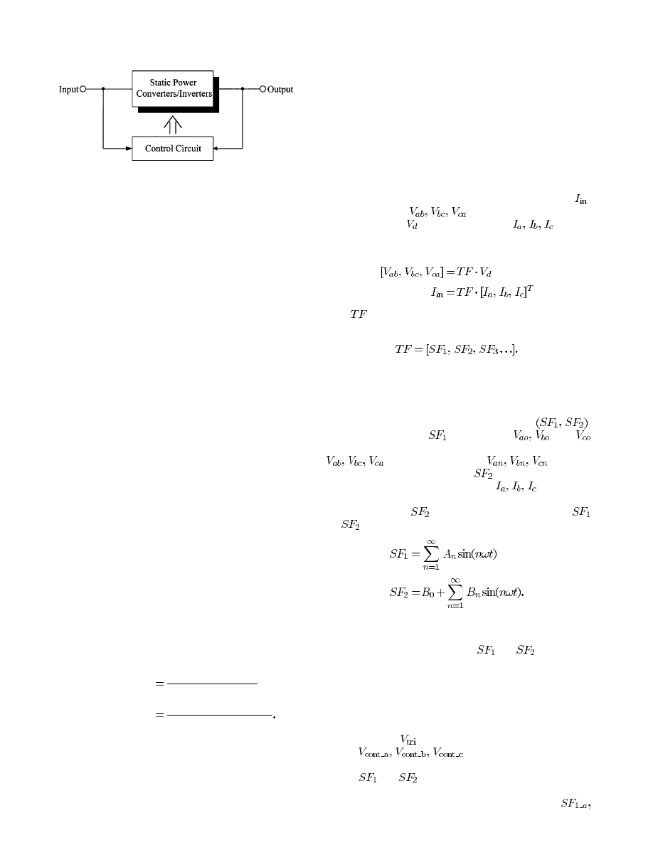
Fig. 1.
Block diagram of the static power conversion system.
performance of control strategy can be effectively exam-
ined without long simulation run time and convergence
problem.
3) The design parameters such as voltage and current ratings
of the power semiconductor switches and load current can
be easily calculated.
4) Obtaining the state equations and using the real power
semiconductor device models are not required in order to
describe the power conversion circuit.
5) The convergence problem is avoided and simulation run
time is greatly reduced.
6) It can be easily extended to different power conversion
topologies, such as pulsewidth-modulation (PWM) ac–dc
rectifier and PWM ac–dc–ac converter.
In the remainder of this paper, the general switching function
concept is reviewed in brief and the proposed functional model
for the VSI and the implementation using Matlab Simulink are
explained in detail. Also, this concept is extended to the voltage-
doubler-type PWM ac–dc rectifier and the PWM ac–dc–ac con-
verter, and, several simulation results are presented to verify the
validity of the proposed models.
II. G
ENERAL
T
HEORY OF
S
WITCHING
F
UNCTION
As shown in Fig. 1, the static power converters/inverters can
be modeled as a black box with the input and output ports. The
dc and ac variables can be input and output according to the
operation mode [4]. Then, the transfer function is obtained to
describe the task to be performed by the circuits. In particular,
the transfer function can be used to compute a dependent vari-
able in terms of its respective independent circuit variable [3].
Also, in PWM, the waveform to be modulated is considered the
independent variable and the resulting modulated waveform is
the dependent variable. For example, in the case of a VSI, the
output voltage is dependent variable and it depends on the input
voltage, which is the independent variable. Therefore, the gen-
eral transfer function can be defined as [3]
Transfer Function
Dependent Variable
Independent Variable
Unmodulated Waveform
Modulated Waveform
(1)
With the applied control strategy, each transfer function con-
sists of the various particular switching functions. Using the
switching function theory, the detailed relationship between the
input and output variables can be obtained. Therefore, obtaining
the proper switching function is very important in order to de-
scribe the role of the static power converters/inverters. The de-
tailed theoretical explanation of the switching function is well
addressed in the references [1]–[3].
III. P
ROPOSED
F
UNCTIONAL
M
ODEL FOR
T
HREE
-P
HASE
V
OLTAGE
S
OURCE
I
NVERTER
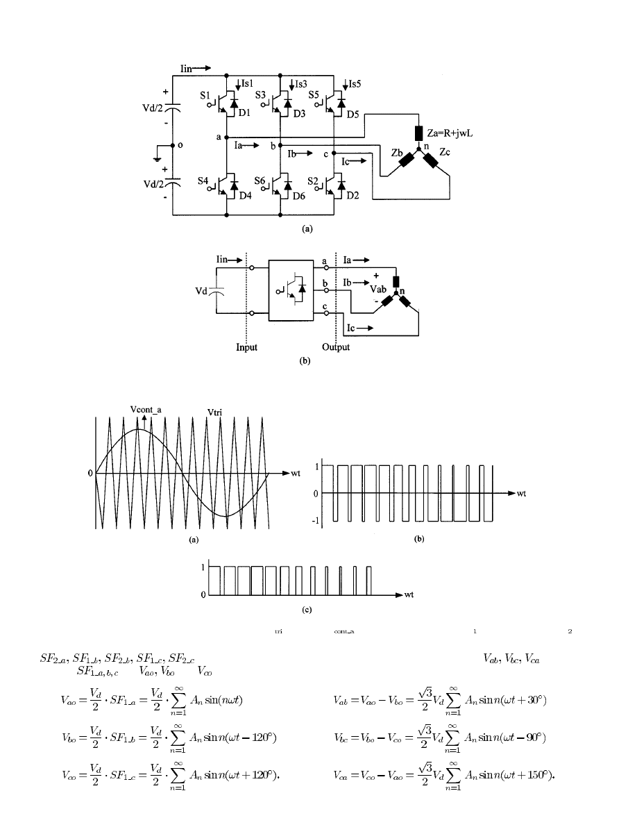
A. Switching Function for VSI
Fig. 2(a) shows the circuit configuration of the VSI and
Fig. 2(b) designates the input and output variables to be
considered in analyzing and designing the circuit. Based on
the transfer function theory, in the VSI, input current (
)
and output voltage (
) are the dependent variables
and input voltage (
) and output current (
) are the
independent variables. Therefore, the relationship between the
input and output variables can be expressed as [3]
(2)
(3)
where
is the transfer function of VSI. Generally, the transfer
function consists of the several switching functions as
(4)
In order to define the switching functions, a control strategy
to be applied should be selected. In this paper, the sinusoidal
PWM (SPWM) technique as shown in Fig. 3(a) is consid-
ered as a control strategy. Based on the SPWM, Fig. 3(b)
and (c) expresses the two switching functions
.
The switching function
expresses the
, and
and it is used to calculate the inverter line-to-line voltages
(
) and phase voltages (
). On the
other hand, the switching function
designates the voltage
across the switch and the load currents (
) are derived
as ratios of voltages and respective impedances using the
switching function
. Mathematical representations
and
are given by [2]
(5)
(6)
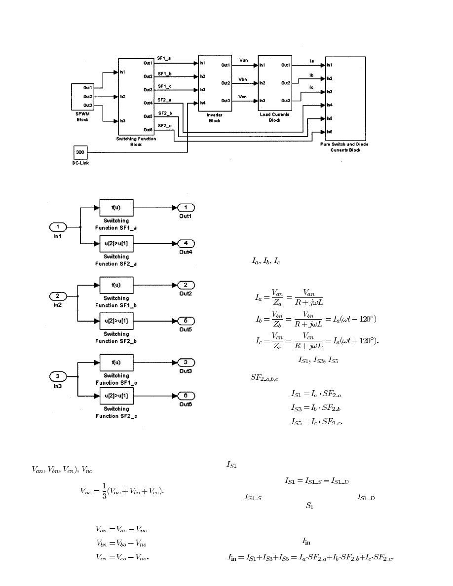
B. Implementation of Functional Model
Based on the switching functions
and
, a functional
model for the VSI is built by using MATLAB Simulink [6].
Fig. 4 shows the proposed overall functional model for calcu-
lating the design parameters of the VSI. As shown in Fig. 4, it
consists of five functional blocks: SPWM generator, switching
function block, inverter block, load current block, and pure
switch and diode current generating block. In the SPWM block,
the carrier signal (
) is compared with three different control
signals (
) and it inputs to the switching
function block to generate the two sets of switching function
signals (
and
) as shown in Fig. 5.
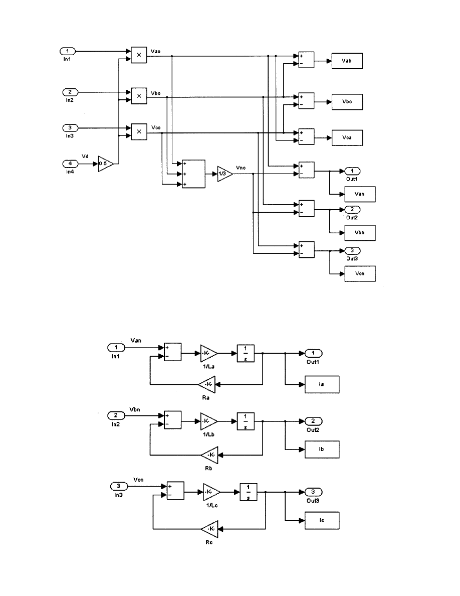
1) Voltage
Variables
(Line-to-Line
and
Phase
Volt-
ages): Each phase has two switching functions such as
LEE AND EHSANI: SIMULATION MODEL FOR THREE-PHASE VSI
311
Fig. 2.
(a) Circuit configuration of VSI. (b) Input and output variables of VSI.
Fig. 3.
SPWM control strategy and switching functions. (a) Carrier (
V ) and control (V
) signals. (b) Switching function
SF . (c) Switching function SF .
. Using the switching
function
, the
, and
can be obtained as
(7)
(8)
(9)
Then, the inverter line-to-line voltages (
) can be
derived as
(10)
312
IEEE TRANSACTIONS ON INDUSTRIAL ELECTRONICS, VOL. 48, NO. 2, APRIL 2001
Fig. 4.
Overall block diagram of the proposed simulation model for VSI using switching function concept.
Fig. 5.
Implementation of switching function block.
Also, in order to calculate the inverter phase voltage
(
is calculated as
(11)
The phase voltages are obtained as
(12)
Based on the above-mentioned theoretical explanation, all the
required voltage variables in the VSI can be obtained, and, it is
realized in the inverter block in Fig. 4 with the proper switching
functions. The detailed description of the inverter block is de-
scribed in Fig. 6.
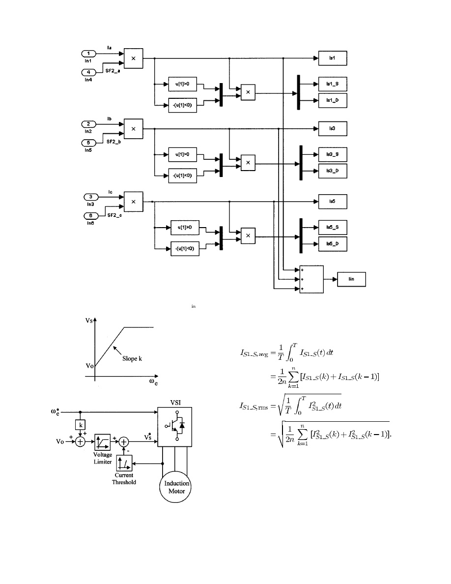
2) Current Variables (Load, Switch, and Inverter Input Cur-
rents): Next, the load current block is used to obtain the load
currents (
). Assuming the load consists of an R-L load
and a balanced one, the load currents are derived as ratios of the
phase voltages and respective impedance as
(13)
The switch currents (
) are calculated by the
product of the load currents with the corresponding switching
function
, that is,
(14)
In order to calculate the current rating of the power semicon-
ductor switch, one needs the information for the pure switch
current and the pure diode current. Actually, the switch current
(
) can be divided into
(15)
where
is the pure switch current and
is the pure
diode current of the switch
. Equations (13)–(15) are imple-
mented in the load current block and the pure current generator
block as shown in Fig. 4 and the actual implementations are des-
ignated as shown in Figs. 7 and 8. Also, from the switch currents,
the inverter input current (
) can be obtained by
(16)
LEE AND EHSANI: SIMULATION MODEL FOR THREE-PHASE VSI
313
Fig. 6.
Inverter line-to-line and phase voltages generating block based on the switching function.
Fig. 7.
Load currents calculating block using the phase voltages.
314
IEEE TRANSACTIONS ON INDUSTRIAL ELECTRONICS, VOL. 48, NO. 2, APRIL 2001
Fig. 8.
Pure switch and diode currents and inverter input current (
I ) generating block.
(a)
(b)
Fig. 9.
Dynamic analysis model of the proposed simulation model using
linearly compensated volts/hertz control.
3) Average and RMS Ratings: Finally, the average and rms
values of current parameters can be expressed by the vector
forms such as (17) and (18) and it can be calculated in the
MATLAB workspace by getting the data from Fig. 4
(17)
(18)
With any kind of control strategy, such as current control,
SPWM, and SVPWM, the final output of the controller is the
proper gate signals, which drive the inverter or converter, to
achieve the desired outputs. These gate signals can be converted
to the switching function signals, which are explained in this
paper. In this paper, we explain how the switching function con-
cept could be used to model the VSI, and, as an example, we use
the SPWM control strategy. Even though SVPWM is used instead
of SPWM, the only change is to replace the SPWM block in Fig. 4
with SVPWM and the outputs of SVPWM block are converted to
the sets of switching function signals in the same manner, and, no
modification is required for the remainder of parts.
LEE AND EHSANI: SIMULATION MODEL FOR THREE-PHASE VSI
315
Fig. 10.
Voltage-doubler ac–dc boost rectifier for power-factor correction.
IV. D
YNAMIC
A
NALYSIS AND
O
THER
E
XAMPLES
A. Dynamic Analysis Model
The speed and torque control loop can be combined with the
proposed model for the dynamic analysis. Fig. 9 shows an ex-
ample of the implementation for the dynamic analysis model
using the volts/hertz speed control algorithm. In Fig. 9, the VSI
block designates the proposed functional model as described in
Fig. 4. With the speed (frequency) and voltage references, the
frequency modulation ratio (
) and the amplitude modulation
ratio (
) are calculated and used as input data of the SPWM
block in Fig. 4, which results in generating the proper gating
signals based on the calculated
and
. Therefore, the dy-
namic response according to the volts/hertz control can be effec-
tively measured. Also, in the same manner, other speed/torque
control algorithms can be implemented without modification of
the proposed static simulation model.
B. Other Examples
As explained earlier, the proposed model can be easily ex-
tended to the other power conversion systems. In this paper, we
present two other examples, such as the voltage-doubler-type
PWM dc–ac rectifier and PWM ac–dc–ac converter.
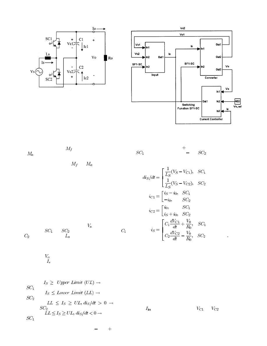
Fig. 10 shows the circuit configuration of the voltage doubler.
As shown in Fig. 10, the ac main source (
) is connected to the
one switch leg (
and
) and one split capacitor leg (
and
) via input inductor
. Therefore, the voltage-doubler
rectifier can be divided into three blocks, such as the ac input
block, converter block, and current controller block as shown in
Fig. 11. The main functions of this rectifier are to maintain the
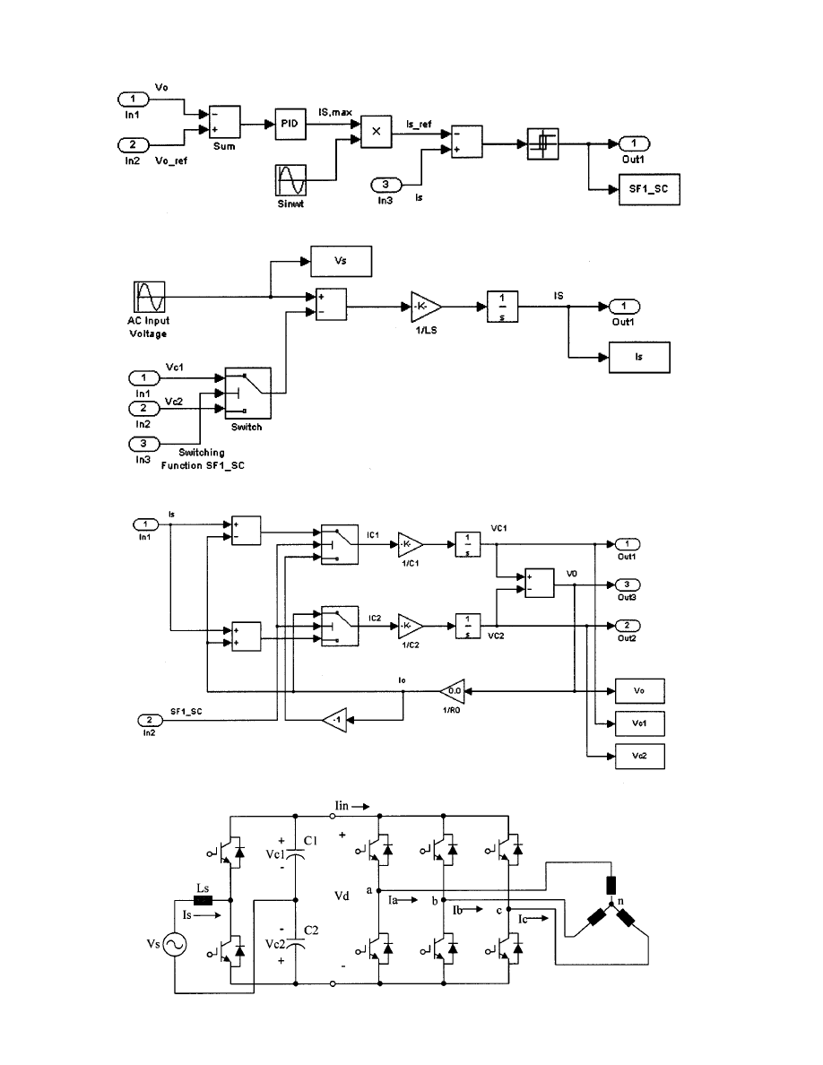
dc-link voltage (
) to a desired constant value and to make the
ac input current ( ) be a sinusoidal waveform for unity power
factor. It is realized by the hysteresis current control method as
shown in Fig. 12. The mechanism of hysteresis current control
can be explained as follows.
• Period I:
Upper Switch
is turned on.
• Period II:
Lower Switch
is turned on.
• Period III:
Lower
Switch
is on.
• Period IV:
Upper Switch
is on.
As a result, the output of the current controller block is the
switching function signal, repeating between
1 and
1, which
Fig. 11.
Block diagram of simulation model for the voltage-doubler rectifier
using switching function.
means that the positive value ( 1) is the turn-on switching status
of
and the negative value ( 1) is
. Then, based on the
switching signal, the detailed voltage and current equations can
be derived as
is turned on
is turned on
(19)
is turned on
is turned on
(20)
is turned on
is turned on
(21)
is turned on
is turned on
(22)
Based on the generated switching function, using (19)–(22), the
overall voltage and current equations can be implemented as
shown in Figs. 13 and 14.
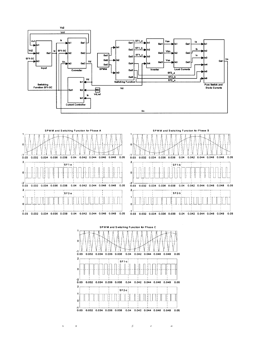
With the developed voltage-doubler rectifier and the VSI
models, the entire PWM ac–dc–ac system for power-factor cor-
rection and speed control can be easily composed. Fig. 15 shows
the circuit configuration and Fig. 16 shows the simulation model
of the PWM ac–dc–ac system. As shown in Fig. 16, the voltage-
doubler rectifier model and the VSI model are connected in series
with a little modification. The only changes are that constant
dc-link voltage is replaced by the instantaneous voltage source,
which is obtained from the voltage doubler, and the inverter input
current (
) is used for calculating the
and
.
Therefore, from this example, it is noted that the developed
simulation model can be easily extended to other power conver-
sion systems with a little modification due to its modular char-
acteristics.
316
IEEE TRANSACTIONS ON INDUSTRIAL ELECTRONICS, VOL. 48, NO. 2, APRIL 2001
Fig. 12.
Hysteresis current controller block.
Fig. 13.
Input block for generating the input current by hysteresis current control.
Fig. 14.
AC–DC boost converter block.
Fig. 15.
PWM ac–dc–ac converter with voltage doubler for power-factor correction and speed control.
LEE AND EHSANI: SIMULATION MODEL FOR THREE-PHASE VSI
317
Fig. 16.
Block diagram of simulation model for PWM ac–dc–ac converter using switching function.
(a)
(b)
(c)
Fig. 17.
Switching function
SF and SF with the SPWM control (parameters: f = 1 kHz, f = 60 Hz, M = 0:8). (a) Phase A. (b) Phase B. (c) Phase C.
318
IEEE TRANSACTIONS ON INDUSTRIAL ELECTRONICS, VOL. 48, NO. 2, APRIL 2001
(a)
(b)
(c)
(d)
Fig. 18.
Voltage and current waveforms of VSI with the SPWM control (parameters:
V = 300 V, f = 1 kHz, f = 60 Hz, Ma = 0:8). (a) V ; V ; V ,
and
V
(b) Line-to-line voltages (
V ; V ; V ) (c) Phase voltages (V ; V ; V ) (d) Load currents (I ; I ; I ).
V. S
IMULATION
R
ESULTS AND
D
ISCUSSION
The proposed model for the VSI is implemented using
MATLAB Simulink (version 5.3.1) and the simulation voltage
and current waveforms are presented in Figs. 17–20. The
simulation parameters are as follows: dc-link input voltage
V,
,
mH, carrier signal frequency
1 kHz, control signal frequency
Hz, and modulation
index
.
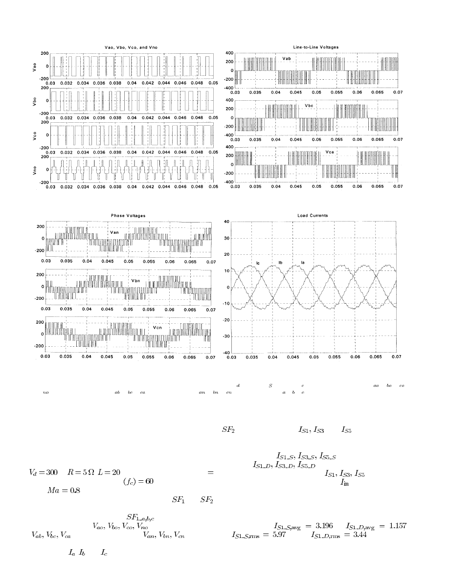
Fig. 17 shows the switching function signals
and
for the three phases, obtained from the SPWM control strategy.
Based on the switching functions
, the inverter voltage
parameters, such as
, line-to-line voltages
(
), and phase voltages (
), can be
successfully derived as shown in Fig. 18. Also, the balanced
load currents
,
, and
are obtained as shown in Fig. 18(d).
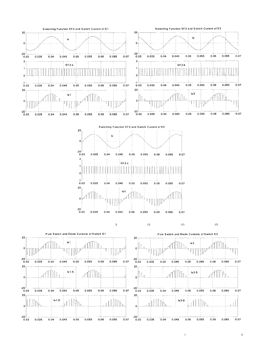
By multiplying the load currents with the switching function
, the switch currents
, and
can be calculated
as shown in Fig. 19. Then, using the pure current-generating
block of Fig. 8, the switch currents are divided into the pure
switch currents (
) and the pure diode
currents (
) as shown in Fig. 20. By
adding the three switch currents (
), the inverter
input current (dc-link output current)
can be composed
as shown in Fig. 20(d). In order to select the proper power
semiconductor device, the voltage and current ratings should
be calculated. Using (17) and (18), the average and rms values
of the currents, which flow through the switch and diode, can
be calculated as
A,
A,
A, and
A. From the
simulation results presented in Figs. 17–20, it is noted that the
proposed functional model perfectly and effectively generates
LEE AND EHSANI: SIMULATION MODEL FOR THREE-PHASE VSI
319
(a)
(b)
(c)
Fig. 19.
Calculating of switch currents using switching function
SF . (a) Switch current I . (b) Switch current I . (c) Switch current I .
(a)
(b)
Fig. 20.
Calculating of pure switch and diode currents and inverter input current. (a) Pure switch and diode currents of
S . (b) Pure switch and diode currents of S .
320
IEEE TRANSACTIONS ON INDUSTRIAL ELECTRONICS, VOL. 48, NO. 2, APRIL 2001
(c)
(d)
Fig. 20.
(Continued.) Calculating of pure switch and diode currents and inverter input current. (c) Pure switch and diode currents of
S (d) Switch current and
inverter input current.
(a)
(b)
(c)
Fig. 21.
Voltage and current waveforms of voltage-doubler PWM ac–dc converter. (a) Input current and switching function. (b) Input voltage and current.
(c) Output voltage (
V ) and its expanded waveform.
LEE AND EHSANI: SIMULATION MODEL FOR THREE-PHASE VSI
321
the overall characteristics of the three-phase VSI, and it allows
the designer to calculate the design parameters at the same time
in the MATLAB environment.
With the transient parameters (step size: 1
s and run time:
80 ms), we measured the simulation run time of the developed
model as being faster, about 10
the case of the Pspice simu-
lation model with the constant dc-link voltage source. Also, if
the constant dc-link source is obtained from the single-phase
rectifier circuit or the PWM rectifier, the simulation run time in
Pspice is dramatically increased and the convergence problem
becomes more serious. However, in the developed model,
adding the rectifier circuits does not cause any harmful effect
to the simulation run time as well as convergence problem.
Therefore, as expected, the developed model is much faster
than the Pspice with the high performance.
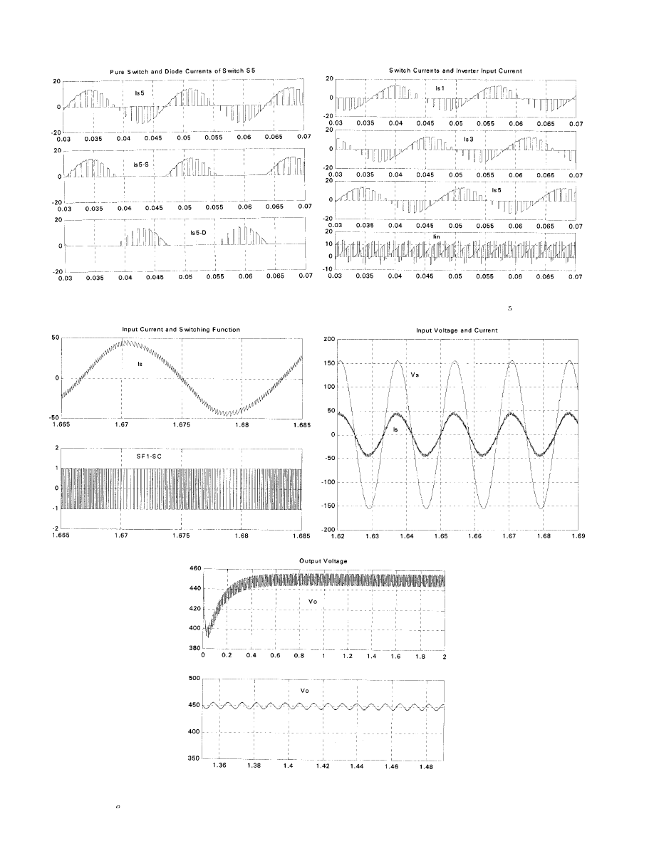
For the developed voltage-doubler-type PWM ac–dc rectifier,
we selected ac input source
V rms/60 Hz, input in-
ductor
mH, and load
, and the voltage and
current waveforms are derived as shown in Fig. 21. Based on the
switching function
, the input current ( ) is synchro-
nized with the input ac source with the sinusoidal waveform,
resulting in unity power factor. Also, with the help of a propor-
tional-plus-integral (PI) controller, dc-link voltage reaches the
reference values with the acceptable voltage ripple. From the
waveforms of Fig. 21, it is noted that the developed model suc-
cessfully outputs the desired characteristics of the voltage-dou-
bler rectifier.
VI. C
ONCLUSIONS
The functional simulation model of a three-phase VSI using
the switching function concept has been studied. The actual im-
plementation of the model has been proposed with the help of
MATLAB Simulink, and this concept was examined in other
power conversion systems.
The general theory of switching functions was reviewed and a
detailed explanation was given for the proposed function model
and its implementation. Also, the validity is verified by several
informative simulation results. Therefore, it is expected that the
proposed model can be effectively utilized in design and ana-
lyzing the power conversion system with various PWM control
techniques. Furthermore, the control strategy to be applied to
the VSI can be easily designed and examined under the devel-
oped functional model.
R
EFERENCES
[1] P. Wood, Theory of Switching Power Converter.
New York: Van Nos-
trand-Reinhold, 1981.
[2] P. D. Ziogas, E. P. Wiechmann, and V. R. Stefanovic, “A computer-aided
analysis and design approach for static voltage source inverter,” IEEE
Trans. Ind. Applicat., vol. IA-21, pp. 1234–1241, Sept./Oct. 1985.
[3] E. P. Wiechmann, P. D. Ziogas, and V. R. Stefanovic, “Generalized func-
tional model for three phase PWM inverter/rectifier converters,” in Conf.
Rrec. IEEE-IAS Annu. Meeting, 1985, pp. 984–993.
[4] L. Salazar and G. Joos, “PSPICE simulation of three-phase inverters by
means of switching functions,” IEEE Trans. Power Electron., vol. 9, pp.
35–42, Jan. 1994.
[5] P. N. Enjeti and P. D. Ziogas, “Analysis of a static power converter under
unbalance: A novel approach,” IEEE Trans. Ind. Electron., vol. 37, pp.
91–93, Feb. 1990.
[6] Matlab Manual Version 5.3.1, The Math Works Inc., Natick, MA, 1998.
Byoung-Kuk Lee (S’94) received the B.S. and M.S.
degrees in electrical engineering from Hanyang Uni-
versity, Seoul, Korea, in 1994 and 1996, respectively.
He is currently working toward the Ph.D. degree at
Texas A&M University, College Station.
His research interests are low-cost reduced parts
converters for ac motor drives, sensorless control
for brushless dc motors, high-frequency resonant
converter systems, and power electronics.
Mehrdad
Ehsani
(S’70–M’81–SM’83–F’96)
received the Ph.D. degree in electrical engineering
from the University of Wisconsin, Madison, in 1981.
Since 1981, he has been with Texas A&M
University, College Station, where he is currently
a Professor of Electrical Engineering and Director
of the Texas Applied Power Electronics Center.
He is the author of more than 200 publications on
pulsed-power supplies, high-voltage engineering,
power electronics, and motor drives. He is the
coauthor of a book on converter circuits for super-
conductive magnetic energy storage and a contributor to an IEEE guide for
self-commutated converters and other monographs. He is the holder of 13
U.S. and EC patents. His current research work is in power electronics, motor
drives, hybrid electric vehicles, and systems.
Dr. Ehsani has been a Member of the IEEE Power Electronics Society (PELS)
AdCom, Past Chairman of the PELS Educational Affairs Committee, Past
Chairman of the Industrial Power Converter Committee of the IEEE Industry
Applications Society (IAS), and Past Chairman of the IEEE Myron Zucker
Student-Faculty Grant Program. He was the General Chair of the IEEE Power
Electronics Specialist Conference for 1990. He is an IEEE Industrial Electronics
Society Distinguished Speaker and IAS Past Distinguished Lecturer. He was
the recipient of Prize Paper Awards in the areas of static power converters and
motor drives at the IAS Annual Meetings in 1985, 1987, and 1992. In 1992, he
was named the Halliburton Professor in the College of Engineering, Texas A&M
University. In 1994, he was also named the Dresser Industries Professor in the
same college. He is a Registered Professional Engineer in the State of Texas.
Wyszukiwarka
Podobne podstrony:
A Composite Pwm Method Of Three Phase Voltage Source Inverter For High Power Applications
A Composite Pwm Method Of Three Phase Voltage Source Inverter For High Power Applications
Control of a single phase three level voltage source inverter for grid connected photovoltaic system
A neural network based space vector PWM controller for a three level voltage fed inverter induction
The Discrete Time Control of a Three Phase 4 Wire PWM Inverter with Variable DC Link Voltage and Bat
The Discrete Time Control of a Three Phase 4 Wire PWM Inverter with Variable DC Link Voltage and Bat
Single Phase Line Frequency Commutated Voltage Source Inverter Suitable for fuel cell interfacing
An Active Power Filter Implemented With A Three Level Npc Voltage Source Inverter
MODELLING GRID CONNECTED VOLTAGE SOURCE INVERTER OPERATION
A Series Active Power Filter Based on a Sinusoidal Current Controlled Voltage Source Inverter
A Series Active Power Filter Based on Sinusoidal Current Controlled Voltage Source Inverter
Algebraic PWM Strategies of a Five Level NYC Voltage Source Inverter
Algebraic PWM Strategies of a Five Level NYC Voltage Source Inverter
A Series Active Power Filter Based on Sinusoidal Current Controlled Voltage Source Inverter
Microprocessor Control System for PWM IGBT Inverter Feeding Three Phase Induction Motor
Adaptive fuzzy control for uninterruptible power supply with three phase PWM inverter
więcej podobnych podstron