TL/F/9774
DM7411
Triple
3-Input
AND
Gate
June 1989
DM7411
Triple 3-Input AND Gate
General Description
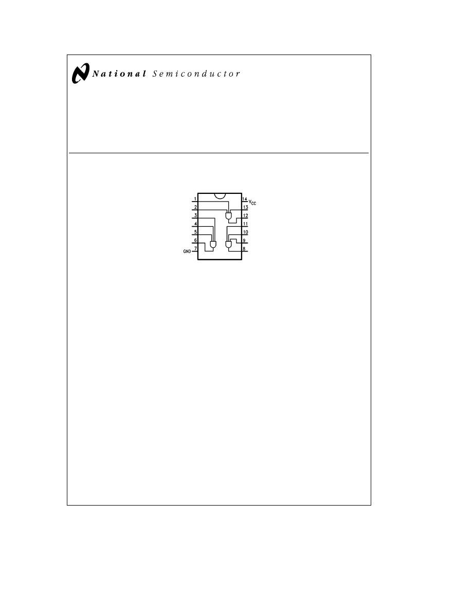
This device contains three independent gates with three
data inputs each which perform the logic AND function.
Connection Diagram
Dual-In-Line Package
TL/F/9774 – 1
Order Number DM7411N
NS Package Number N14A
C1995 National Semiconductor Corporation
RRD-B30M115/Printed in U. S. A.
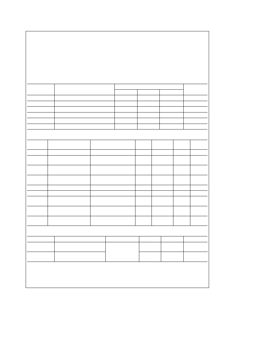
Absolute Maximum Ratings
(Note)
If Military/Aerospace specified devices are required,
please contact the National Semiconductor Sales
Office/Distributors for availability and specifications.
Supply Voltage
7V
Input Voltage
5.5V
Operating Free Air
Temperature Range (DM74)
0
§
C to
a
70
§
C
Storage Temperature Range
b
65
§
C to
a
150
§
C
Note:
The ‘‘Absolute Maximum Ratings’’ are those values
beyond which the safety of the device cannot be guaran-
teed. The device should not be operated at these limits. The
parametric values defined in the ‘‘Electrical Characteristics’’
table are not guaranteed at the absolute maximum ratings.
The ‘‘Recommended Operating Conditions’’ table will define
the conditions for actual device operations.
Recommended Operating Conditions
Symbol
Parameter
DM7411
Units
Min
Typ
Max
V
CC
Supply Voltage
4.75
5
5.25
V
V
IH
High Level Input Voltage
2
V
V
IL
Low Level Input Voltage
0.8
V
I
OH
High Level Output Current
b
0.4
mA
I
OL
Low Level Output Current
16
mA
T
A
Free Air Operating Temperature
0
70
§
C
Electrical Characteristics
over recommended operating free air temperature range (unless otherwise noted)
Symbol
Parameter
Conditions
Min
Typ
Max
Units
(Note 1)
V
I
Input Clamp Voltage
V
CC
e
Min, I
I
e b
12 mA
b
1.5
V
V
OH
High Level Output
V
CC
e
Min, I
OH
e
Max,
2.4
3.4
V
Voltage
V
IL
e
Max
V
OL
Low Level Output
V
CC
e
Min, I
OL
e
Max,
0.2
0.4
V
Voltage
V
IH
e
Min
I
I
Input Current
@
Max
V
CC
e
Max, V
I
e
5.5V
1
mA
Input Voltage
I
IH
High Level Input Current
V
CC
e
Max, V
I
e
2.4V
40
m
A
I
IL
Low Level Input Current
V
CC
e
Max, V
I
e
0.4V
b
1.6
mA
I
OS
Short Circuit
V
CC
e
Max
b
18
b
57
mA
Output Current
(Note 2)
I
CCH
Supply Current with
V
CC
e
Max
15
mA
Outputs High
I
CCL
Supply Current with
V
CC
e
Max
24
mA
Outputs Low
Switching Characteristics
at V
CC
e
5V and T
A
e
25
§
C (See Section 1 for Test Waveforms and Output Load)
Symbol
Parameter
Conditions
Min
Max
Units
t
PLH
Propagation Delay Time
C
L
e
15 pF,
27
ns
Low to High Level Output
R
L
e
400X
t
PHL
Propagation Delay Time
19
ns
High to Low Level Output
Note 1:
All typicals are at V
CC
e
5V, T
A
e
25
§
C.
Note 2:
Not more than one output should be shorted at a time.
2
Wyszukiwarka
Podobne podstrony:
7411
7411
praca-magisterska-7411, Dokumenty(2)
7411
7411
7411
7411
7411
7411
P 775 ED tcm16 7411
7411
więcej podobnych podstron