© 2001 Fairchild Semiconductor Corporation
DS006497
www.fairchildsemi.com
December 1986
Revised July 2001
DM7407 Hex Buff
ers w
it
h
Hi
gh
V
o
lt
age Open-Col
le
ctor
Outp
uts
DM7407
Hex Buffers with High Voltage Open-Collector Outputs
General Description
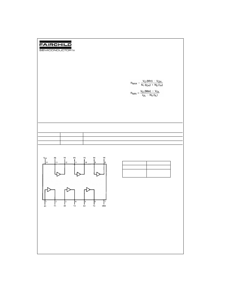
This device contains six independent gates each of which
performs a buffer function. The open-collector outputs
require external pull-up resistors for proper logical opera-
tion.
Pull-Up Resistor Equations
Where: N
1
(I
OH
)
=
total maximum output high current
for all outputs tied to pull-up resistor
N
2
(I
IH
)
=
total maximum input high current for
all inputs tied to pull-up resistor
N
3
(I
IL
)
=
total maximum input low current for
all inputs tied to pull-up resistor
Ordering Code:
Devices also available in Tape and Reel. Specify by appending the suffix letter “X” to the ordering code.
Connection Diagram
Function Table
Y
=
A
H
=
HIGH Logic Level
L
=
LOW Logic Level
Order Number
Package Number
Package Description
DM7407M
M14A
14-Lead Small Outline Integrated Circuit (SOIC), JEDEC MS-012, 0.150" Narrow
DM7407N
N14A
14-Lead Plastic Dual-In-Line Package (PDIP), JEDEC MS-001, 0.300" Wide
Input
Output
A
Y
L
L
H
H
www.fairchildsemi.com
2
D
M
7407
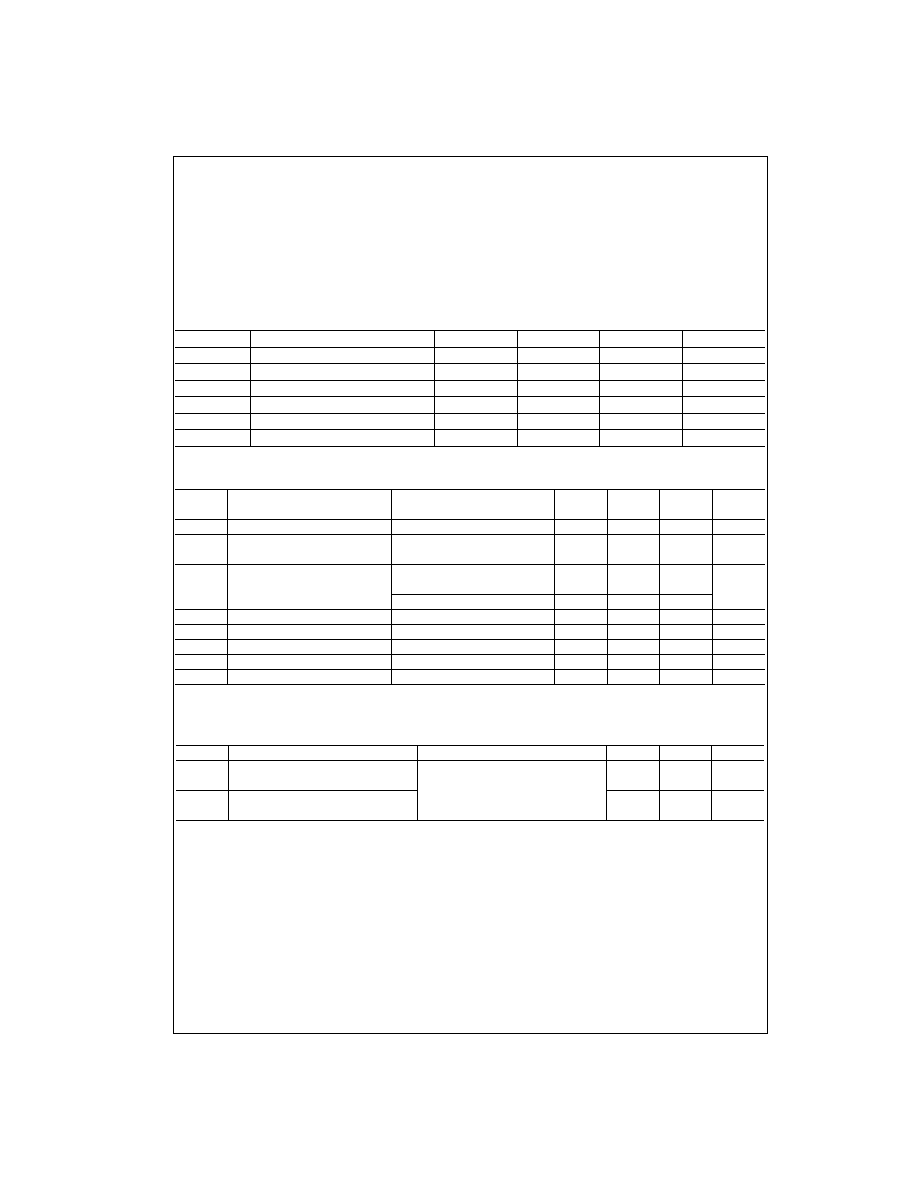
Absolute Maximum Ratings
(Note 1)
Note 1: The “Absolute Maximum Ratings” are those values beyond which
the safety of the device cannot be guaranteed. The device should not be
operated at these limits. The parametric values defined in the Electrical
Characteristics tables are not guaranteed at the absolute maximum ratings.
The “Recommended Operating Conditions” table will define the conditions
for actual device operation.
Recommended Operating Conditions
Electrical Characteristics
over recommended operating free air temperature range (unless otherwise noted)
Note 2: All typicals are at V
CC
=
5V, T
A
=
25
°
C.
Switching Characteristics
at V
CC
=
5V and T
A
=
25
°
C
Supply Voltage
7V
Input Voltage
5.5V
Output Voltage
30V
Operating Free Air Temperature Range
0
°
C to
+
70
°
C
Storage Temperature Range
−
65
°
C to
+
150
°
C
Symbol
Parameter
Min
Nom
Max
Units
V
CC
Supply Voltage
4.75
5
5.25
V
V
IH
High Level Input Voltage
2
V
V
IL
Low Level Input Voltage
0.8
V
V
OH
High Level Output Voltage
30
V
I
OL
Low Level Output Current
40
mA
T
A
Free Air Operating Temperature
0
70
°
C
Symbol
Parameter
Conditions
Min
Typ
Max
Units
(Note 2)
V
I
Input Clamp Voltage
V
CC
=
Min, I
I
=
−
12 mA
−
1.5
V
I
CEX
HIGH Level
V
CC
=
Min, V
O
=
30V
250
µ
A
Output Current
V
IH
=
Min
V
OL
LOW Level
V
CC
=
Min, I
OL
=
Max
0.7
Output Voltage
V
IL
=
Max
V
I
OL
=
16 mA, V
CC
=
Min
0.4
I
I
Input Current @ Max Input Voltage
V
CC
=
Max, V
I
=
5.5V
1
mA
I
IH
HIGH Level Input Current
V
CC
=
Max, V
I
=
2.4V
40
µ
A
I
IL
LOW Level Input Current
V
CC
=
Max, V
I
=
0.4V
−
1.6
mA
I
CCH
Supply Current with Outputs HIGH
V
CC
=
Max
29
41
mA
I
CCL
Supply Current with Outputs LOW
V
CC
=
Max
21
30
mA
Symbol
Parameter
Conditions
Min
Max
Units
t
PLH
Propagation Delay Time
C
L
=
15 pF
10
ns
LOW-to-HIGH Level Output
R
L
=
110
Ω
t
PHL
Propagation Delay Time
30
ns
HIGH-to-LOW Level Output
3
www.fairchildsemi.com
DM7407
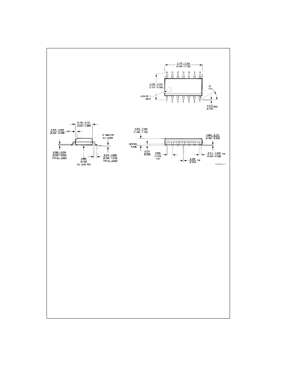
Physical Dimensions
inches (millimeters) unless otherwise noted
14-Lead Small Outline Integrated Circuit (SOIC), JEDEC MS-012, 0.150" Narrow
Package Number M14A
www.fairchildsemi.com
4
DM
7
407
Hex Buff
ers
wit
h
H
igh V
o
lt
a
ge
Open-
Coll
ect
or O
u
tputs
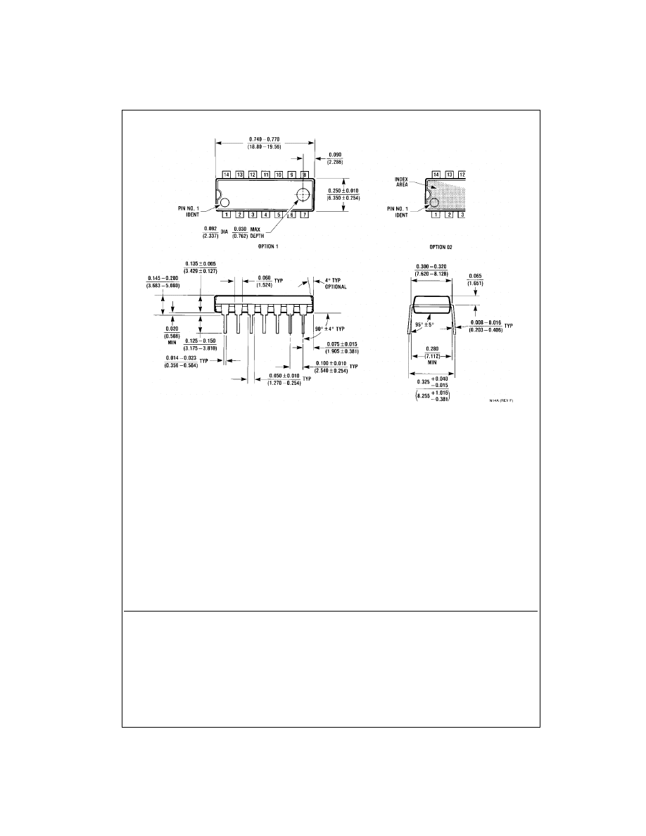
Physical Dimensions
inches (millimeters) unless otherwise noted (Continued)
14-Lead Plastic Dual-In-Line Package (PDIP), JEDEC MS-001, 0.300" Wide
Package Number N14A
Fairchild does not assume any responsibility for use of any circuitry described, no circuit patent licenses are implied and
Fairchild reserves the right at any time without notice to change said circuitry and specifications.
LIFE SUPPORT POLICY
FAIRCHILD’S PRODUCTS ARE NOT AUTHORIZED FOR USE AS CRITICAL COMPONENTS IN LIFE SUPPORT
DEVICES OR SYSTEMS WITHOUT THE EXPRESS WRITTEN APPROVAL OF THE PRESIDENT OF FAIRCHILD
SEMICONDUCTOR CORPORATION. As used herein:
1. Life support devices or systems are devices or systems
which, (a) are intended for surgical implant into the
body, or (b) support or sustain life, and (c) whose failure
to perform when properly used in accordance with
instructions for use provided in the labeling, can be rea-
sonably expected to result in a significant injury to the
user.
2. A critical component in any component of a life support
device or system whose failure to perform can be rea-
sonably expected to cause the failure of the life support
device or system, or to affect its safety or effectiveness.
www.fairchildsemi.com
Wyszukiwarka
Podobne podstrony:
SN7403 1 QUADRUPOLE 2 INPUT POSITIVE NAND GATES WITH OPEN COLLECTOR OUTPUT
SN7401 1 QUADRUPOLE 2 INPUT POSITIVE NAND GATES WITH OPEN COLLECTOR OUTPUTS
Ir2111 High Voltage High Speed Power Mosfet And Igbt Driver
15 185 196 A ew High Tensile Steel with High Toughness
A ZVS PWM Inverter With Active Voltage Clamping Using the Reverse Recovery Energy of the Diodes
[DI] Circuit makes simple high voltage inverter
MCP16301 High Voltage Input Integrated Switch Step Down Regulator
High voltage electrostatic generator
05 Integrated High Voltage Electronics to drive Microactuators
Differences in the note taking skills of students with high achievement,
Preparation of garlic powder with high allicin content by using combined microwave–vacuum and vacuum
Make your Own High Voltage Electromagnets
High voltage electrostatic generator
Parameters od model luminaire with high power LED diodes
więcej podobnych podstron