
EPSON IMPACT DOT PRINTER
DLQ-3000
(upgrade model)
SERVICE MANUAL
EPSON
4006094

PREFACE
This document provides supplementary information to describe the new DLQ-3000 (Minerva+), which is a
follow-on version of the DLQ-3000 (Minerva). Therefore, you must refer to this information in conjunction with
DLQ-3000 (Minerva) Service Manual for details on any subjects common to both printers.
-i-
REVISION SHEET
Revision
Issue Date
Revision Page
A
March 15, 1996
-
1st issue
-ii-

1.1 FEATURES
Minerva+ is a 24-pin serial dot-matrix and flat-bed type impact printer. As this printer follows on DLQ-3000
(MINERVA+), the main future is almost same as DLQ-3000 (MINERVA).
The main features are ;
❏
Two built-in and one optional I/F
Bi-Directional Parallel Interface (IEEE-1284 nibble mode)
Serial Interface
Type-B Interface (Option)
The exterior view of DLQ-3000 (MINERVA+) is the same as DLQ-3000 (MINERVA).
DLQ-3000 (MINERVA+)
Product Description
Rev.A
1-1
1.2 INTERFACE OVERVIEW
The printer provides an 8-bit Bi-directional parallel interface and serial interface as standard. Moreover, it is
possible to interface to various computers using the optional type-B interface board. This section describes
the specifications of the standard interfaces.
1.2.1 Parallel Interface Specifications
1.2.1.1 Forward Channel
Transmission mode:
8-bit parallel, IEEE-1284 compatible mode
Synchronization:
By STROBE pulse
Handshaking:
By BUSY and ACKNLG signal
Signal level:
TTL-compatible level, IEEE-1284 level 1 device
Adaptable connector:
57-30360 (Amphenol) or equivalent
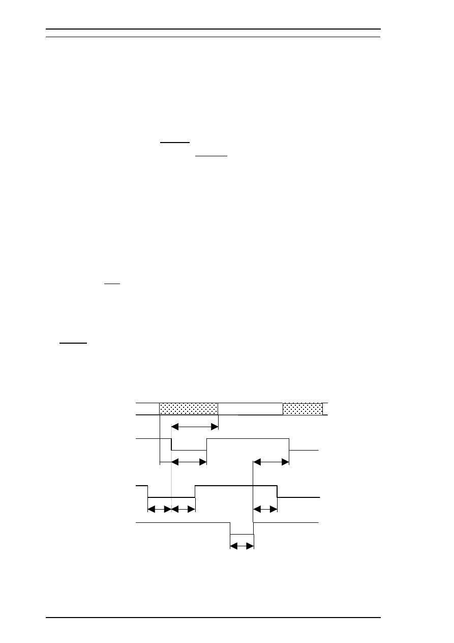
Data transmission timing:
See Figure 1-1.
Note:
Transition time (rise time and fall time) of every input signal must be less than 200 ns and
every output signal must be less than 120 ns.
The BUSY signal is at a HIGH level before either -ERROR signal is at a LOW level or the PE signal is at a
HIGH level until all these signals return to their inactive state. The BUSY signal is at a HIGH level in the
following cases:
-
During data reception (see the figure above)
-
When the input buffer is full
-
When the INIT input signal is active
-
During initialization
-
When the ERROR signal is active
-
In the self-test mode
-
In the SelecType
-
When the parallel interface is not selected.
The ERROR signal is at a LOW level when the printer is in one of the following conditions:
-
Printer hardware error (fatal error)
-
A paper-out error
-
Release lever operation error
PE signal is at a HIGH level during paper out error.
DATA (n)
D ATA
-STORBE
B U S Y
-AC KNLG
500 ns (min.)
500 ns (min.)
500 ns (min.)
0 (min.)
0 (min.)
500 ns ~10 µs
0 (min.)
500 ns (max.)
DATA (n+1)
Figure 1-1. Data Transmission Timing
Product Description
DLQ-3000 (MINERVA+)
1-2
Rev.A
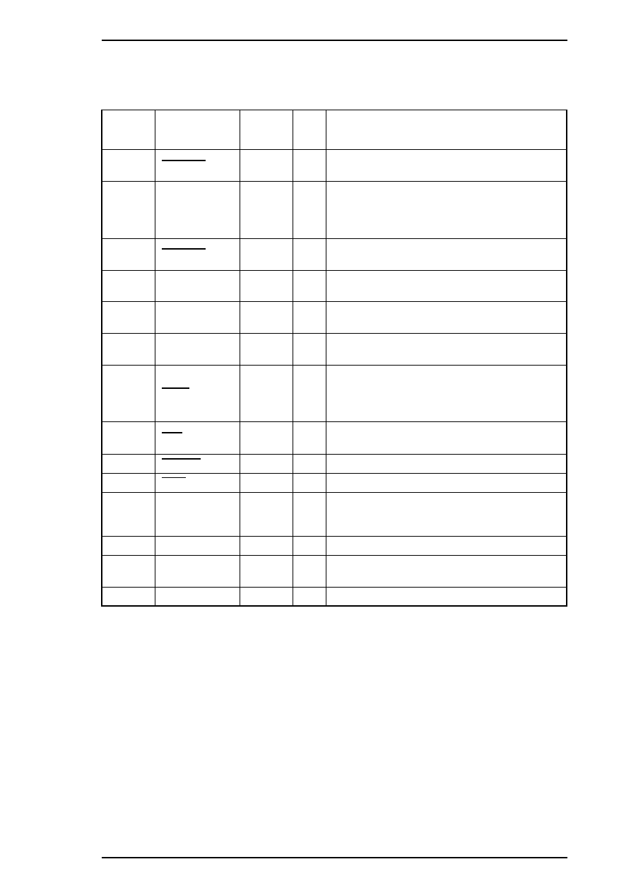
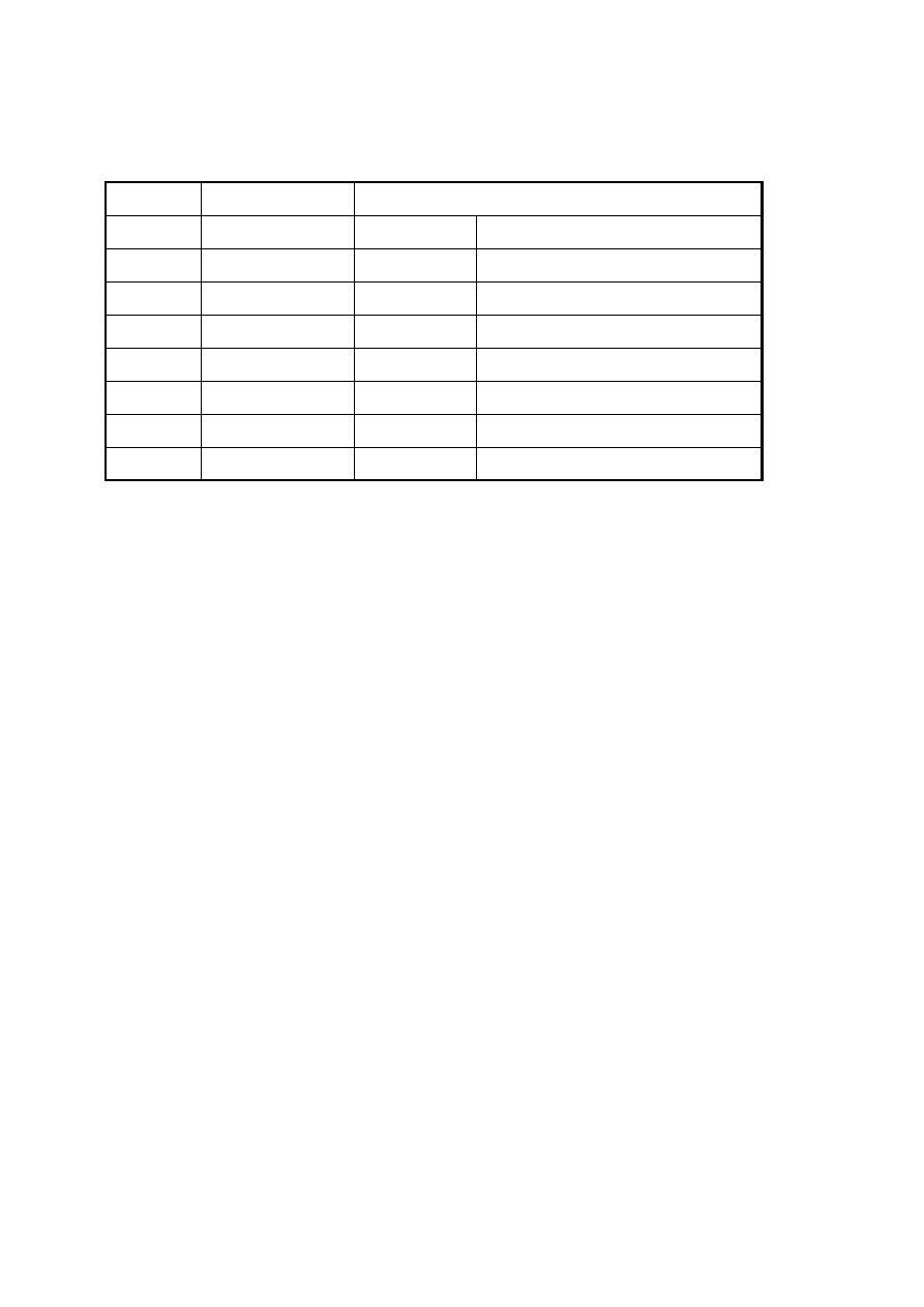
Table 1-1 shows the connector pin assignments and signal functions for the 8-bit parallel interface.
Table 1-1. Signal and Connector Pin Assignments for Parallel Interface
(Forward Channel)
Pin No.
Signal Name
Return
GND Pin
I/O
Description
1
STROBE
19
In
Strobe pulse. Input data is latched at the falling
edge of this signal.
2-9
DATA1-8
20-27
In
Parallel input data to the printer.
Active-HIGH input.
LSB:
DATA1
MSB:
DATA8
10
ACKNLG
28
Out
Indicates that data has been received and the
printer is ready to accept more data.
11
BUSY
29
Out
A HIGH level means the printer cannot accept
further data.
12
PE
30
Out
A HIGH level means a paper-out error. Always
the logical opposite of the ERROR signal.
13
SLCT
-
Out
Always at a HIGH level (pulled up to +5 V
through a 1K-ohm resistor).
14
AFXT
-
In
Auto feed execution means that a line feed is
automatically performed upon input of a CR
code. Checked when the printer is initialized.
Active-LOW signal.
31
INIT
16
In
Initialize printer. Minimum 50
µ
s pulse is
necessary. Active-LOW signal.
32
ERROR
-
Out
A LOW level means that an error has occurred.
36
SLIN
30
In
Not used.
18,35
Logic H
-
Out
Pulled up to +5V and shorted to +5V via Schottky
diode, making these signals appear low to the
host when the printer is turned off.
17
Chassis GND
-
-
Chassis GND
16,19-30,
33
GND
-
-
Signal GND
15,34
NC
-
-
Not used. Not connected.
Note:
In/Out refers to the direction of signal flow as viewed from the printer.
DLQ-3000 (MINERVA+)
Product Description
Rev.A
1-3
1.2.1.2 Reverse Channel
Transmission mode:
8-bit parallel, IEEE-1284 nibble mode
Synchronization:
Refer to the IEEE-1284 specification
Handshaking:
Refer to the IEEE-1284 specification
Signal level:
IEEE-1284 level 1 device
Data transmission timing:
Refer to the IEEE-1284 specification
Extensibility request:
the printer responds to the extensibility request in the affirmative, when the
request is 00H or 04H, which mean;
00H:
Request nibble mode of reverse channel transfer
04H:
Request device ID in nibble mode of reverse channel
Transfer Device ID:
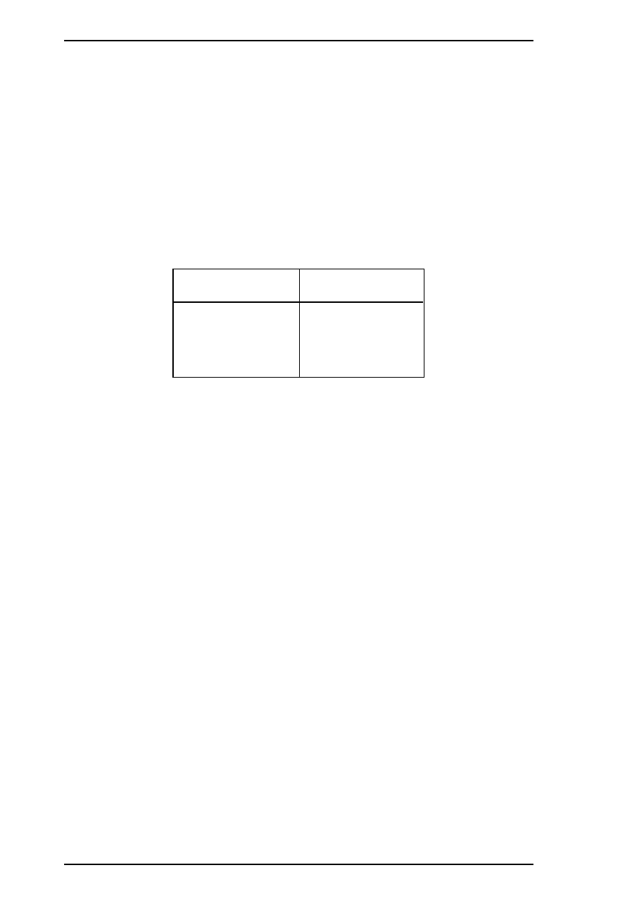
Table 1-2. Transfer ID
ESC/P2
IBM 2391 Plus
[00H][33H]
MFG:EPSON;
CMD:ESCPL2-00;
MDL:DLQ-3000;
CLS:PRINTER;
[00H][34H]
MFG:EPSON;
CMD:PRPXL24-01;
MDL:DLQ-3000;
CLS:PRINTER;
Product Description
DLQ-3000 (MINERVA+)
1-4
Rev.A
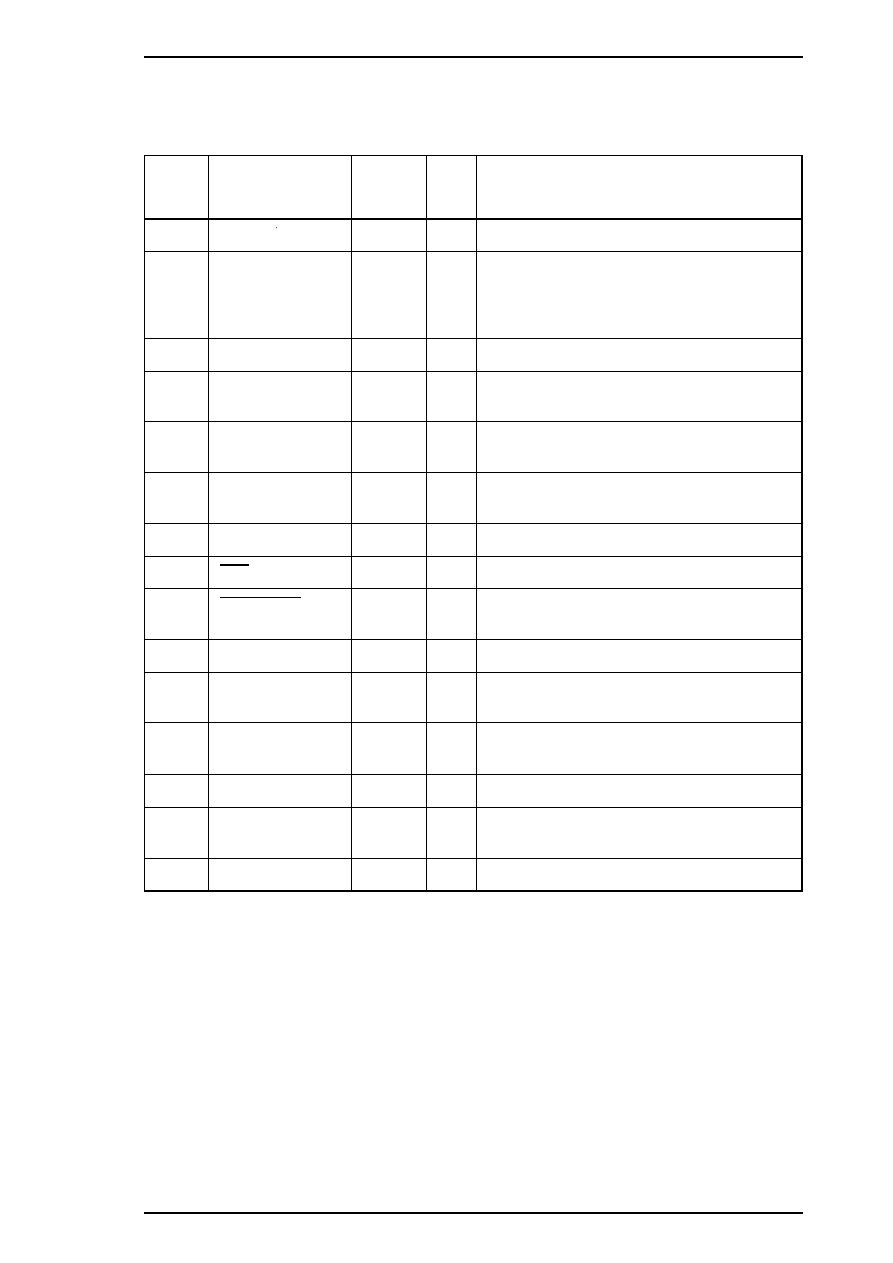
Table 1-3 shows the connector pin assignments and signal functions for the 8-bit parallel interface.
Table 1-3. Signal and Connector Pin Assignments for Parallel Interface
(Reverse Channel)
Pin No.
Signal Name
Return
GND Pin
I/O
Description
1
Host Clk
19
In
Host clock signal.
2-9
DATA 1-8
20-27
In
Parallel input data to the printer.
Active-HIGH input.
LSB:
DATA1
MSB:
DATA8
10
Ptr Clk
28
Out
Printer clock signal
11
PtrBusy /
Data Bit -3,7
29
Out
Printer BUSY signal and reverse channel
transfer data bit 3 or 7.
12
Ack Data Req /
Data Bit -2,6
28
Out
Acknowledge data request signal and reverse
channel transfer data bit 2 or 6.
13
Xflag /
Data Bit -1,5
28
Out
Xflag signal and reverse channel transfer data
bit 1 or 5.
14
Host Busy
30
In
Host busy signal
31
INIT
30
In
Not used.
32
Data Avail /
Data Bit -0,4
29
Out
Data available signal and reverse channel
transfer data bit 0 or 4.
36
1284-Active
30
In
1284 active signal
18
Logic H
-
Out
A high signal indicates that all other signals
source by the peripheral are in a valid state.
35
+5V
-
Out
This line is pulled up to +5V through 3.3K
Ω
resister.
17
Chassis
-
-
Chassis GND
16,19-30
,33
GND
-
-
Signal GND
15,34
NC
-
-
Not used. Not connected.
Note:
In/Out refers to the direction of signal flow as viewed from the printer.
DLQ-3000 (MINERVA+)
Product Description
Rev.A
1-5

1.5 MAIN COMPONENTS
The main components of the DLQ-3000 are designed for easy removal and repair. The main components are
:
■ BOARD ASSY., C124 MAIN-B :
control board
■ BOARD ASSY., C124 PSB/PSE :
power supply board(100 ~ 120V/220 ~ 240V)
■ C124 SUB board
■ M-5L60 Printer Mechanism
■ Control Panel
■ Housing
1.5.1 BOARD ASSY., C124 MAIN-B
The main board consists of a
µ
PD70433, an E05A88, Program (256 KB Flash memory), CG (8M for Japan /
4 M for other countries), D-RAMs (256 MB), Bi-Directional Interface circuit, etc.
1.5.2 BOARD ASSY., C124 PSB/PSE
This Power supply board consists of two transformers, two switching FETs, a switching regulator IC, diode
bridge, etc. This board has ratings for input AC voltages.
1.5.3 Printer Mechanism
This printer mechanism consists of a 24-pin impact dot head, PF motor , CR motor, color ribbon shift motor,
HP/PG sensor, paper width/paper end sensor, etc.
1.4.5 Housing Assembly
This printer Housing consists of the COVER ASSY.,PRINTER, the HOUSING ASSY.,UPPER, the
HOUSING ASSY.,LOWER and FRAME ASSY.,BOTTOM.
Product Description
DLQ-3000 (MINERVA+)
1-6
Rev.A
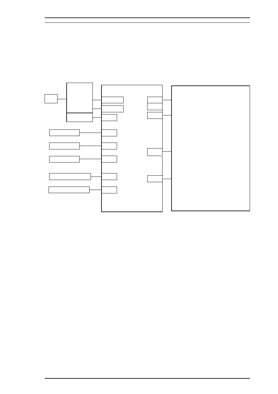
A.1 CONNECTOR SUMMARY
This section describes the component connection and detailed pin assignments of each connector of the units.
Figure A-1 shows the component connections of the DLQ-3000, and Table A-1 lists the connector
assignments and reference tables.
TYPE-B I/F
PARALLEL I/F
CN1 0 -1 2
SERIA L I/F
C N 7
C N 8
C N 6
C N 9
C N 1
C N 2
C N 3
C N 4
CN 5
C N 1 3
C N 1 4
CN 15, 16
temp.
A C
Fan motor
C 12 4P S B/PSE
Printer M echan ism
C1 2 4 M AIN - B
P a n e l
Cover O pen S ensor
P rint head
C S M o t o r
Film Ribb on S e nsor
Color Ribb o n S en sor
P E WS en sor A s semb ly
CR Mot or Assembly
P F Motor Assembly
LO A D S ensor A sse mbly
E xt ern al Fan
P F S e nsor
HP S ens or
Figure A-1. Cable Connection
DLQ-3000 (MINERVA+) Service Manual
Appendix
Rev.A
A-1
Table A-2 through appendix lists connector pin assignments.
Table A-1. Connector Assignment
Board
Connector
Pin
Description
BOARD
ASSY.,C124
MAIN-B
CN 1
20
Printhead drive signal output
CN 2
20
Printhead drive signal output
CN 3
14
CS motor, Color ribbon / film ribbon / CS home sensor
CN 4
11
CR motor, PF motor output
CN 5
13
PG/ REL/COVER OPEN/LOAD sensor, External fan motor
CN 6
36
Type -B I/F
CN 7
36
Bi-Directional parallel I/F
CN 8
25
Serial I/F
CN 9
2
Power supply board fan motor
CN 10
4
Power supply input (+5V)
CN 11
6
Power supply input (+35V)
CN 12
6
Power supply input (+35V)
CN 13
10
Control panel
CN 14
2
CR motor common (cover open sensor)
CN 15
2
Power supply board temp.
CN 16
2
Power supply board temp.
C124 SUB
BOARD
CN 4
From CN1 to Printhead output signal
CN 5
From CN2 to Printhead output signal
CN 6
From CN3 to CS motor, Color ribbon / film ribbon / CS
home sensor
BOARD
ASSY., C124
PSB / PSE
CN 1
2
AC input line
CN 2
10
DC output ( +5V, +35V )
CN 3
6
DC output ( +35V )
Appendix
DLQ-3000 (MINERVA+) Service Manual
A-2
Rev.A
Table A-2. Connector Pin Assignment - CN7
Pin
I/O
Name
Description (Forward / Reverse)
1
I
STOBE / Host
Clk
Data strobe / Host clock signal
2 - 9
I
DATA 0-7
Parallel data bit 0 to 7
10
O
ACKNLG /
PtrClk
Acknowledge / Printer clock signal
11
O
BUSY /
PtrBusy, Data
Bit-3,7
Printer busy and reverse channel transfer data bit 3 or 7
12
O
PE /
AckDataReq,
Data Bit-2,6
Paper out / Acknowledge data request and reverse channel
transfer data bit 2 or 6
13
O
SLCT / Xflag,
Data Bit-1,5
Always HIGH at printer power on / Xflag and reverse
channel transfer data bit 1 or 5
14
I
AFXT / Host
Busy
Not used / Host busy signal
15
-
NC
Not used and not connected.
16
-
GND
Signal Ground
17
-
Chassis GND
Chassis ground
18
O
Logic-H
Pulled up 5V / A HIGH signal indicates that all other signals
soursed by the peripheral are in valid state.
19-30
-
GND
Signal Ground
31
I
INIT / INIT
Initialize signal / Not used
32
O
ERROR / data
avail, data
bit-0,4
Error signal / Data available and reverse channel data bit 0,4
33
-
GND
Signal Ground
34
-
NC
Not used and not connected.
35
O
+5V
Pulled up 5V
36
I
SLIN /
1284-Active
Not used. / 1284-active signal
Note:
The signal direction I/O are viewed from the connector on the board.
DLQ-3000 (MINERVA+) Service Manual
Appendix
Rev.A
A-3
COM14 20
COM1 0/1 8 13
COM6/22 2
COM2 14
COM23 10
COM3/19 4
COM7/15 6
COM11 3
20 COM14
13 COM10/18
2 COM6/22
14 COM2
10 COM23
4 COM3/19
6 COM7/15
3 COM11
HD2 17
HD3 9
HD6 15
HD7 19
HD10 1 6
HD11 1 1
HD14 1 2
HD15 1
HD18 1 8
HD19 8
HD22 7
HD23 5
17 HD2
9 HD3
15 HD6
19 HD7
16 HD10
11 HD11
12 HD14
1 HD15
18 HD18
8 HD19
7 HD22
5 HD23
C N 1
He ad Con n 1
from mainboard
C N 4
Head c onn 1
to H ea d
COM12 /16 10
COM8/20 15
COM4/24 11
COM1/21 1
COM5/17 7
COM9/13 2
10 COM12/16
15 COM8/20
11 COM4/24
1 COM1/21
7 COM5/17
2 COM9/13
HD1 13
HD4 17
HD5 3
HD8 18
HD9 5
HD12 12
HD13 4
HD16 16
HD17 5
HD20 9
HD21 8
HD24 14
TE NP 19
TE MP 20
13 HD1
17 HD4
3 HD5
18 HD8
5 HD9
12 HD12
4 HD13
6 HD16
5 HD17
9 HD20
8 HD21
14 HD24
19 TEMP
20 TEMP
C N 2
Head Conn 2
from mainboard
C N 5
Hea d con n 2
to Head
+5V 1
PEWR/L 5
PWLCOM 6
PW RC OM 2
RFCOM 7
RFA 11
RF_A 9
RFB 10
RF_B 8
CSHOME 3
GND 4
COLOR 13
FILM 14
GND 12
1 +5v
5 PEWR/L
5 PWLCOM
2 PWRCOM
7 RFCOM
11 RFA
9 RF_A
10 RFB
8 RF_B
3 CSHOME
4 GND
13 COLOR
14 FILM
12 GND
C N 1
Head Con n 1
from mainboard
C N 4
H e a d c o n n 1
to H e ad
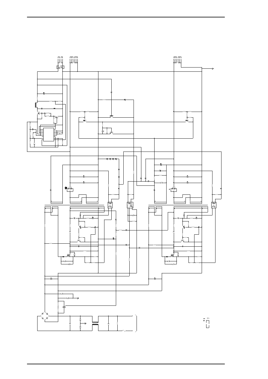
Figure A-4. C124 MAIN SUB Board Circuit Diagram
DLQ-3000 (MINERVA+) Service Manual
Appendix
Rev.A
A-9
-0
0
4
2
W
L
1
5
1
L
P
2
0
1
-2
R
5
S
D
Q
1
5
1
A
1
4
6
9
R
1
5
3
0
.2
2
D
1
5
5
E
R
C
8
1
R
1
5
2
R
1
6
4
1
0
0
C
1
5
4
1
0
0
0
u
1
0
V
X
2
R
1
5
8
1
0
0
K
C
1
5
9
5
6
0
p
+
I
1
1
- I
1
2
F B
3
D T C
4
C T
5
R T
6
G N D
7
C
1
8
+
I
2
1 6
- I
2
1 5
R O
1 4
O C
1 3
V C C
1 2
C
2
1 1
E
2
1 0
E 1
9
IC
1
5
1
T
L
4
9
4
R
1
6
1
2
0
R
1
6
2
3
0
0
Z
D
1
5
5
H
Z
S
6
A
1
L
R
1
6
0
1
0
K
R
1
5
1
4
7
0
/2
W
R
1
5
9
4
.7
5
K
R
1
8
1
8
4
.5
K
D
1
5
2
E
R
A
8
2
-0
0
4
1
4
6
T
1
0
1
5
7
R
1
3
1
0
.2
2
/2
W
R
1
1
8
1
0
0
K
/1
W
C
1
1
1
5
6
0
u
/2
0
0
V
1
3
2
4
D
B
1
0
1
R
B
V
-2
5
0
6
*
T
F
C
3
3
3
0
0
p
C
4
3
3
0
0
p
C
2
0
.2
2
u
T
Y
1
0
1
S
M
1
2
G
Z
4
7
A
R
3
2
.2
5
W
R
2
2
.2
5
W
C
8
2
2
0
0
p
C
3
1
2
2
0
0
p
C
1
1
6
3
3
0
0
p
/1
.2
K
V
*
F
B
1
0
1
Q
1
0
1
K
1
8
5
5
C
1
1
4
4
7
0
0
p
Q
1
0
2
C
4
4
0
8
Q
1
0
3
A
1
0
1
5
D
1
0
2
1
S
S
1
2
0
R
1
1
5
2
7
0
C
1
1
3
0
.1
u
R
1
1
6
2
7
0
C
1
1
5
3
3
0
0
p
/1
.2
K
V
R
1
1
1
3
0
0
/1
W
D
1
0
1
E
R
A
8
2
-0
0
4
1
0
4
1
2
1
3
3
D
1
3
1
E
R
A
8
2
-0
0
4
1
3
2
D
1
5
1
F
1
0
P
1
0
Q
R
1
7
0
1
0
K
Q
1
5
2
A
1
6
8
0
R
1
6
6
2
0
0
K
R
1
6
7
3
K
C
1
5
8
0
.0
1
u
R
1
6
3
3
.6
K
R
1
7
2
5
.6
K
B
1
5
1
R
1
6
5
1
k
G
L
+
5
V
/1
.0
A
2
3
4
5
6
7
8
1
C
N
2
+
3
5
V
/1
.5
A
c
h
.B
1
0
G
p
B
9
C
1
8
1
0
.1
u
R
1
7
3
1
.2
K
R
1
7
1
1
.5
k
R
1
8
2
2
K
Q
1
5
3
A
1
0
1
5
C
1
5
7
4
7
0
u
/6
.3
V
R
1
7
4
1
0
K
R
1
7
5
2
.7
K
C
1
5
1
R
1
5
6
3
0
0
Z
D
1
8
5
H
Z
S
6
A
-2
Z
D
1
8
4
H
Z
S
6
A
-2
C
1
5
2
3
3
0
0
u
/5
0
V
X
2
2
5
V
R
1
1
3
4
.7
k
R
1
1
7
1
C
1
1
2
1
0
0
u
1
2
4
3
P
C
1
0
1
T
L
P
5
2
1
-1
9
2
1
1
1
R
1
1
4
2
7
0
2
1
3
IC
1
0
1
N
J
M
4
3
1
R
1
1
9
1
0
K
R
1
1
2
0
.3
0
/3
W
R
1
2
1
4
.7
K
R
1
2
0
2
.4
K
C
1
0
.6
8
u
1
2
3
4
L
1
E
L
F
1
8
D
8
50
C
N
L
R
1
3
9
0
K
2
1
C
N
1
F
1 1
0
A
/1
2
5
V
D
1
0
4
E
R
B
4
3
-0
4
R
1
2
6
1
0
0
K
/1
W
R
1
2
4
2
2
0
/2
W
C
1
1
7
2
2
0
0
U
/1
6
V
R
1
2
3
3
9
D
2
0
3
E
R
A
8
2
-0
0
4
R
2
3
2
1
1
2
6
5
4
P
C
1
0
2
T
L
P
5
4
1
G
R
1
2
5
2
7
K
R
1
5
7
5
1
0
R
1
6
8
1
0
k
C
1
1
8
0
.0
1
u
D
1
0
3
E
R
A
8
2
-0
0
4
R
1
3
2
1
D
1
8
1
1
S
S
1
2
0
Z
D
1
5
1
H
Z
S
6
A
-2
Z
D
1
8
1
H
Z
S
6
A
-2
Z
D
1
8
2
H
Z
S
6
A
-2
Z
D
1
8
3
H
Z
S
6
A
-2
R
1
6
9
5
1
0
Q
1
5
4
C
1
8
1
5
Q
1
5
5
D
T
C
1
1
4
E
S
Z
D
1
5
3
H
Z
S
7
B
-2
Z
D
1
5
2
R
D
3
9
J
S
A
B
3
D
2
5
4
1
S
S
1
2
0
D
1
5
3
1
S
S
1
2
0
R
1
5
4
2
K
R
1
5
5
2
0
K
Z
D
1
5
4
H
Z
S
6
A
-2
C
1
5
6
3
3
u
/1
6
V
C
1
5
5
0
.1
u
D
1
5
4
1
S
S
1
2
0
D
2
5
2
E
R
A
8
2
-0
0
4
4
1
4
6
T
2
0
1
5
7
R
2
3
1
0
.2
2
/2
W
D
2
0
4
E
R
B
4
3
-0
4
R
2
1
8
1
0
0
k
/1
W
C
2
1
1
5
6
0
u
/2
0
0
V
C
2
1
6
3
3
0
0
p
/1
.2
K
V
*
B
2
0
1
Q
2
0
1
K
1
8
5
5
C
2
1
4
4
7
0
0
p
Q
2
0
2
C
4
4
0
8
Q
2
0
3
A
1
0
1
5
R
2
1
5
2
7
0
R
2
1
4
2
7
0
F
D
2
0
2
1
S
S
1
2
0
R
2
1
9
1
0
K
C
2
1
3
0
.1
u
R
2
1
6
2
7
0
R
2
2
1
4
.7
K
C
2
1
5
3
3
0
0
p
/1
.2
K
V
D
2
0
1
E
R
A
8
2
-0
0
4
R
2
1
3
4
.7
k
R
2
1
7
1
R
2
1
1
3
0
0
/1
W
1
0
9
1
2
1
3
3
D
2
3
1
E
R
A
8
2
-0
0
4
F
1
3
2
D
2
5
1
F
1
0
P
1
0
Q
C
2
5
1
C
2
5
2
3
3
0
0
u
/5
0
V
X
2
R
2
7
0
1
0
K
Q
2
5
3
A
1
0
1
5
R
2
7
1
1
.5
k
R
2
7
2
5
.6
K
R
2
7
3
1
.2
K
1
C
N
3
2
3
6
5
4
+
3
5
V
/1
.5
A
c
h
.A
G
p
A
R
2
5
6
3
0
0
D
2
8
1
1
S
S
1
2
0
2
5
V
C
2
1
2
1
0
0
u
1
2
4
3
P
C
2
0
1
T
L
P
5
2
1
-1
R
2
5
7
5
1
0
2
1
1
1
2
1
3
IC
2
0
1
N
J
M
4
3
1
R
2
1
2
0
.3
0
/3
W
R
2
2
0
2
.4
K
(T
Y
1
0
1
,Q
1
0
1
,Q
2
0
1
,D
1
5
1
,D
2
5
1
)
(C
1
8
1
)
H
e
a
ts
in
k
N
o
t
m
o
u
n
te
d
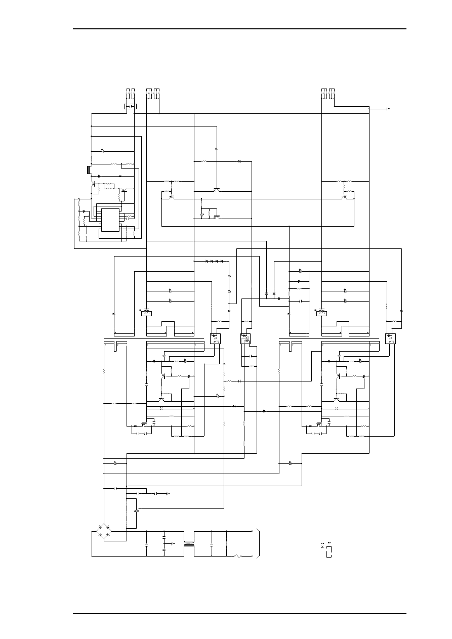
Figure A-5. C124 PSB Board Circuit Diagram
Appendix
DLQ-3000 (MINERVA+) Service Manual
A-10
Rev.A
-0
0
4
2
W
L
1
5
1
L
P
2
0
1
-2
R
5
S
D
Q
1
5
1
A
1
4
6
9
R
1
5
3
0
.2
2
D
1
5
5
E
R
C
8
1
R
1
5
2
R
1
6
4
1
0
0
C
1
5
4
1
0
0
0
u
1
0
V
X
2
R
1
5
8
1
0
0
K
C
1
5
9
5
6
0
p
+
I
1
1
- I
1
2
F B
3
D T C
4
C T
5
R T
6
G N D
7
C 1
8
+
I
2
1 6
- I
2
1 5
R O
1 4
O C
1 3
V C C
1 2
C 2
1 1
E 2
1 0
E 1
9
IC
1
5
1
T
L
4
9
4
R
1
6
1
2
0
R
1
6
2
3
0
0
R
1
6
0
1
0
K
R
1
5
1
4
7
0
/2
W
R
1
8
1
8
4
.5
K
R
1
5
9
4
.7
5
K
Z
D
1
5
5
H
Z
S
6
A
1
L
D
1
5
2
E
R
A
8
2
-0
0
4
1
4
6
T
1
0
1
5
7
R
1
3
1
0
.2
2
/2
W
R
1
2
8
1
0
0
K
/1
W
C
1
1
1
1
5
0
u
/4
0
0
V
C
3
1
4
7
0
0
p
1
3
2
4
D
B
1
0
1
D
5
S
B
A
6
0
*
T
Y
1
0
1
S
M
8
JZ
4
7
A
5
W
C
3
4
7
0
0
p
C
4
4
7
0
0
p
C
2
0
.2
2
u
R
2
4
.7
T
F
R
3
4
.7
5
W
R
4
4
.7
5
W
C
8
4
7
0
0
p
C
9
4
7
0
0
p
*
F
B
1
0
1
Q
1
0
1
K
1
6
9
2
C
1
1
4
4
7
0
0
p
Q
1
0
2
C
4
4
0
8
Q
1
0
3
A
1
0
1
5
D
1
0
2
1
S
S
1
2
0
R
1
1
5
2
7
0
C
1
1
3
0
.1
u
R
1
1
6
2
7
0
R
1
1
8
1
0
0
K
/1
W
C
1
1
5
3
3
0
0
p
/1
.2
K
V
C
1
1
6
3
3
0
0
p
/1
.2
K
V
R
1
1
1
3
0
0
/1
W
D
1
0
1
E
R
A
8
2
-0
0
4
1
0
4
1
2
1
3
3
D
1
3
1
E
R
A
8
2
-0
0
4
1
3
2
D
1
5
1
F
1
0
P
1
0
Q
R
1
7
0
1
0
K
Q
1
5
2
A
1
6
8
0
R
1
6
6
2
0
0
K
R
1
6
7
3
K
C
1
5
8
0
.0
1
u
R
1
6
3
3
.6
K
R
1
7
2
5
.6
K
B
1
5
1
R
1
6
5
1
k
G
L
+
5
V
/1
.0
A
2
3
4
1
0
5
8
6
9
7
c
h
.B
1
C
N
2
+
3
5
V
/1
.5
A
G
p
B
C
1
8
1
0
.1
u
R
1
7
3
1
.2
K
R
1
7
1
1
.5
k
R
1
8
2
2
K
Q
1
5
3
A
1
0
1
5
C
1
5
7
4
7
0
u
/6
.3
V
R
1
7
4
1
0
K
R
1
7
5
2
.7
K
C
1
5
1
R
1
5
6
3
0
0
Z
D
1
8
5
H
Z
S
6
A
-2
Z
D
1
8
4
H
Z
S
6
A
-2
C
1
5
2
3
3
0
0
u
/5
0
V
X
2
2
5
V
R
1
1
3
4
.7
k
R
1
1
7
1
C
1
1
2
1
0
0
u
1
2
5
4
P
C
1
0
1
T
L
P
6
3
4
9
1
2
1
1
R
1
1
4
2
7
0
2
1
3
IC
1
0
1
N
JM
4
3
1
R
1
1
9 10
K
R
1
1
2
0
.6
8
/3
W
R
1
2
1
4
.7
K
R
1
2
0
2
.4
K
C
1
0
.6
8
u
1
2
3
4
L
1
E
L
F
1
8
D
8
5
0
Z
N
L
1
C
N
1
2
F
1
T
5
A
H
/2
5
0
V
R
1
3
9
0
K
/0
.5
W
R
1
2
7
1
0
0
K
/1
W
D
1
0
4
E
R
B
3
8
-0
5
R
1
2
6
1
0
0
K
/1
W
R
1
2
4
2
2
0
/2
W
R
1
2
3
3
9
C
1
1
7
2
2
0
0
u
/1
6
V
D
2
0
3
E
R
A
8
2
-0
0
4
R
2
3
2
1
C
1
1
8
0
.0
1
u
R
1
2
5
1
0
K
R
1
5
7
5
1
0
R
1
6
8
1
0
k
1
2
6
5
4
P
C
1
0
2
T
L
P
6
4
7
J
(D
4
-L
F
2
)
(D
4
-G
B
-L
F
2
)
D
1
0
3
E
R
A
8
2
-0
0
4
R
1
3
2
1
D
1
8
1
1
S
S
1
2
0
Z
D
1
5
1
H
Z
S
6
A
-2
Z
D
1
8
1
H
Z
S
6
A
-2
Z
D
1
8
2
H
Z
S
6
A
-2
Z
D
1
8
3
H
Z
S
6
A
-2
R
1
6
9
5
1
0
Q
1
5
4
C
1
8
1
5
Q
1
5
5
D
T
C
1
1
4
E
S
Z
D
1
5
3
H
Z
S
7
B
-2
Z
D
1
5
2
R
D
3
9
J
S
A
B
3
F
D
2
5
4
1
S
S
1
2
0
D
1
5
3
1
S
S
1
2
0
C
1
5
5
0
.1
u
R
1
5
4
2
K
R
1
5
5
2
0
K
Z
D
1
5
4
H
Z
S
6
A
-2
C
1
5
6
3
3
u
/1
6
V
D
1
5
4
1
S
S
1
2
0
D
2
5
2
E
R
A
8
2
-0
0
4
4
1
4
6
T
2
0
1
5
7
R
2
3
1
0
.2
2
/2
W
D
2
0
4
E
R
B
3
8
-0
5
R
2
2
8
1
0
0
K
/1
W
C
2
1
1
1
5
0
u
/4
0
0
V
*
B
2
0
1
Q
2
0
1
K
1
6
9
2
C
2
1
4
4
7
0
0
p
Q
2
0
2
C
4
4
0
8
Q
2
0
3
A
1
0
1
5
R
2
1
5
2
7
0
R
2
1
4
2
7
0
F
D
2
0
2
1
S
S
1
2
0
R
2
1
9
1
0
K
C
2
1
3
0
.1
u
R
2
1
6
2
7
0
R
2
1
8
1
0
0
K
/1
W
R
2
2
1
4
.7
K
C
2
1
5
3
3
0
0
p
/1
.2
K
V
C
2
1
6
3
3
0
0
p
/1
.2
K
V
D
2
0
1
E
R
A
8
2
-0
0
4
R
2
1
3
4
.7
k
R
2
1
7
1
R
2
1
1
3
0
0
/1
W
1
0
9
1
2
1
3
3
D
2
3
1
E
R
A
8
2
-0
0
4
1
3
2
D
2
5
1
F
1
0
P
1
0
Q
C
2
5
1
C
2
5
2
3
3
0
0
u
/5
0
V
X
2
R
2
7
0
1
0
K
Q
2
5
3
A
1
0
1
5
R
2
7
1
1
.5
k
R
2
7
2
5
.6
K
R
2
7
3
1
.2
K
2
3
4
5
6
c
h
.A
+
3
5
V
/1
.5
A
1
C
N
3
G
p
A
R
2
5
6
3
0
0
D
2
8
1
1
S
S
1
2
0
2
5
V
C
2
1
2
1
0
0
u
R
2
5
7
5
1
0
1
2
5
4
P
C
2
0
1
T
L
P
6
3
4
1
2
1
1
2
1
3
IC
2
0
1
N
J
M
4
3
1
R
2
2
0
2
.4
K
R
2
1
2
0
.6
8
/3
W
(T
Y
1
0
1
,Q
1
0
1
,Q
2
0
1
,D
1
5
1
,D
2
5
1
)
(C
1
8
1
)
(D
4
-G
B
-L
F
2
)
H
e
a
ts
in
k
N
o
t
m
o
u
n
te
d
Figure A-6. C124 PSE Board Circuit Diagram
DLQ-3000 (MINERVA+) Service Manual
Appendix
Rev.A
A-11

EPSON
Document Outline
- DLQ-3000 Service Manual
- Front Cover
- Preface
- Revision Sheet
- 1.1 Features
- 1.2 Interface Overview
- 1.5 Main Components
- A.1 Connector Summary
- Back Cover
Wyszukiwarka
Podobne podstrony:
Epson Stylus Color 460 Service Manual
Epson Stylus Pro XL Service Manual
Epson Stylus Color 300 Service Manual
Epson Stylus Color 700 Stylus Color EX Service Manual
hplj 5p 6p service manual vhnlwmi5rxab6ao6bivsrdhllvztpnnomgxi2ma vhnlwmi5rxab6ao6bivsrdhllvztpnnomg
Oberheim Prommer Service Manual
Korg SQ 10 Service Manual
MAC1500 service manual
Kyocera Universal Feeder UF 1 Service Manual
Proview RA783 LCD Service Manual
indesit witp82euy Service Manual
Glow Worm installation and service manual Hideaway 70CF UIS
Proview PZ456 LCD Service Manual
Glow Worm installation and service manual Ultimate 50CF UIS
więcej podobnych podstron