TA8264AH
2002-02-13
1
TOSHIBA Bipolar Linear Integrated Circuit Silicon Monolithic
TA8264AH
Max Power 41 W BTL × 4 ch Audio Power IC
The TA8264AH is 4 ch BTL audio power amplifier for car audio
application.
This IC can generate more high power: P
OUT
MAX = 41 W as it
is included the pure complementary PNP and NPN transistor
output stage.
It is designed low distortion ratio for 4 ch BTL audio power
amplifier, built-in stand-by function, muting function, and
diagnosis circuit which can detect output to V
CC
/GND short and
over voltage input mode.
Additionally, the AUX amplifier and various kind of protector
for car audio use are built-in.
Features
· High power : P
OUT
MAX (1) = 41 W (typ.)
(V
CC
= 14.4 V, f = 1 kHz, JEITA max, R
L
= 4 Ω)
:
P
OUT
MAX (2) = 37 W (typ.)
(V
CC
= 13.7 V, f = 1 kHz, JEITA max, R
L
= 4 Ω)
:
P
OUT
(1) = 24 W (typ.)
(V
CC
= 14.4 V, f = 1 kHz, THD = 10%, R
L
= 4 Ω)
:
P
OUT
(2) = 21 W (typ.)
(V
CC
= 13.2 V, f = 1 kHz, THD = 10%, R
L
= 4 Ω)
· Built-in diagnosis circuit (pin 25)
· Low distortion ratio: THD = 0.02% (typ.)
(V
CC
= 13.2 V, f = 1 kHz, P
OUT
= 5 W, R
L
= 4 Ω)
· Low noise: V
NO
= 0.18 mV
rms
(typ.)
·
(V
CC
= 13.2 V, R
g
= 0 Ω, G
V
= 34dB, BW = 20 Hz~20 kHz)
· Built-in stand-by switch function (pin 4)
· Built-in muting function (pin 22)
· Built-in AUX amplifier from single input to 2 channels output (pin 16)
· Built-in various protection circuit
: Thermal shut down, over voltage, out to GND, out to V
CC
, out to out short, speaker burned
· Operating supply voltage: V
CC (opr)
= 9~18 V
Weight: 7.7 g (typ.)

TA8264AH
2002-02-13
2
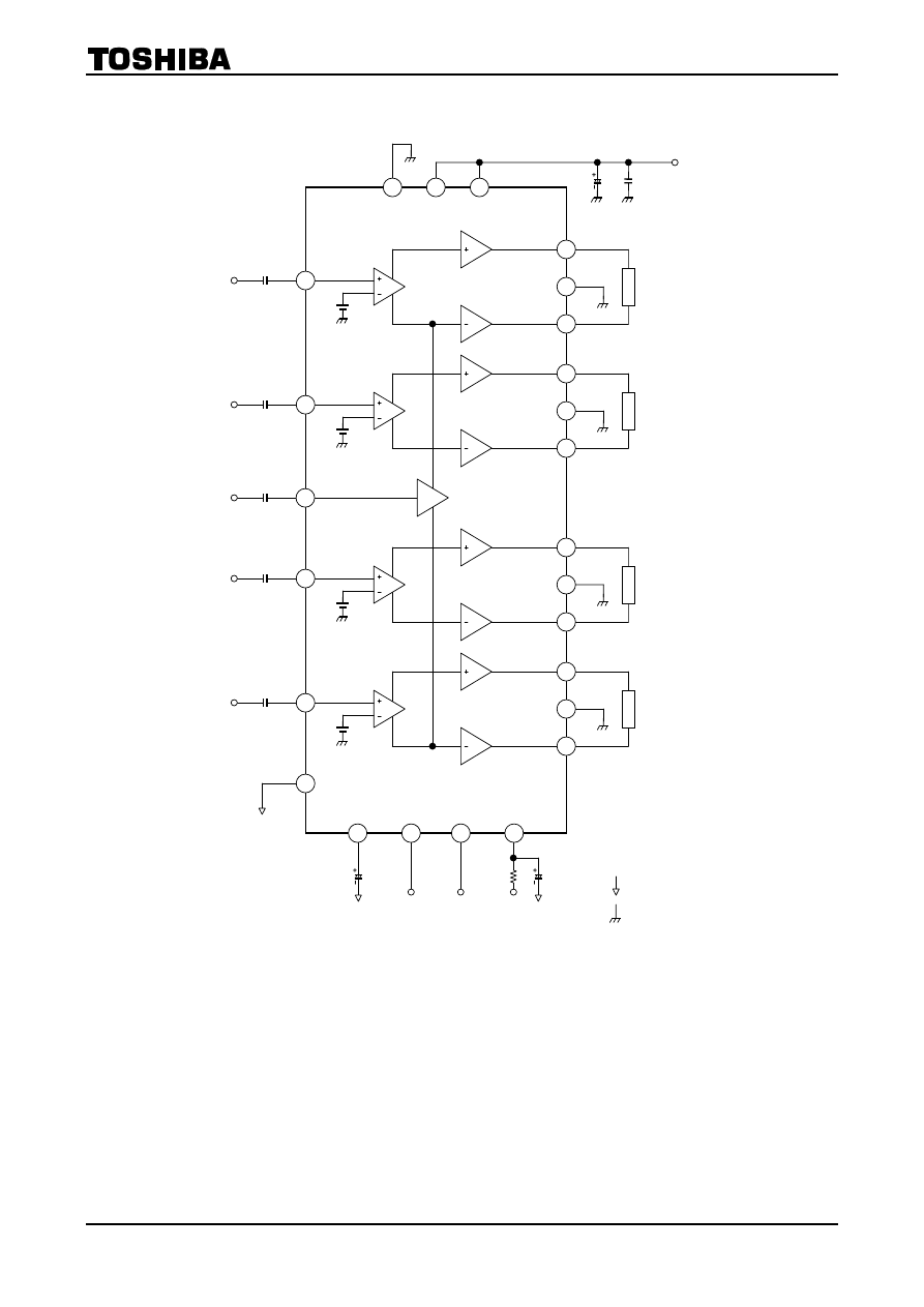
Block Diagram
R
L
R
L
R
L
11
9
8
7
5
2
3
17
18
19
21
24
23
12
15
14
1
20
6
R
L
IN1
IN2
IN3
AUX IN
IN4
13
16
C
1
C
1
C
1
C
1
PRE-GND
10
25
4
22
OUT1 (
+)
PW-GND1
OUT1 (
-)
OUT2 (
+)
PW-GND2
OUT2 (
-)
OUT3 (
+)
PW-GND3
OUT3 (
-)
OUT4 (
+)
PW-GND4
OUT4 (
-)
TAB
V
CC1
V
CC2
C
3
R
1
C
4
C
2
: PRE-GND
: PW-GND
STBY
DIAGNOSIS
OUT
RIP MUTE
C
5
C
6
TA8264AH
2002-02-13
3
Caution and Application Method
(Description is made only on the single channel.)
1. Voltage
Gain
Adjustment
This IC has no NF (negative feedback) terminals. Therefore, the voltage gain can’t adjusted, but it makes
the device a space and total costs saver.
The voltage gain of Amp.1
: G
V1
= 8dB
The voltage gain of Amp.2A, B
: G
V2
= 20dB
The voltage gain of BLT Connection : G
V (BTL)
= 6dB
Therefore, the total voltage gain is decided by expression below.
G
V
= G
V1
+ G
V2
+ G
V (BTL)
= 8 + 20 + 6 = 34dB
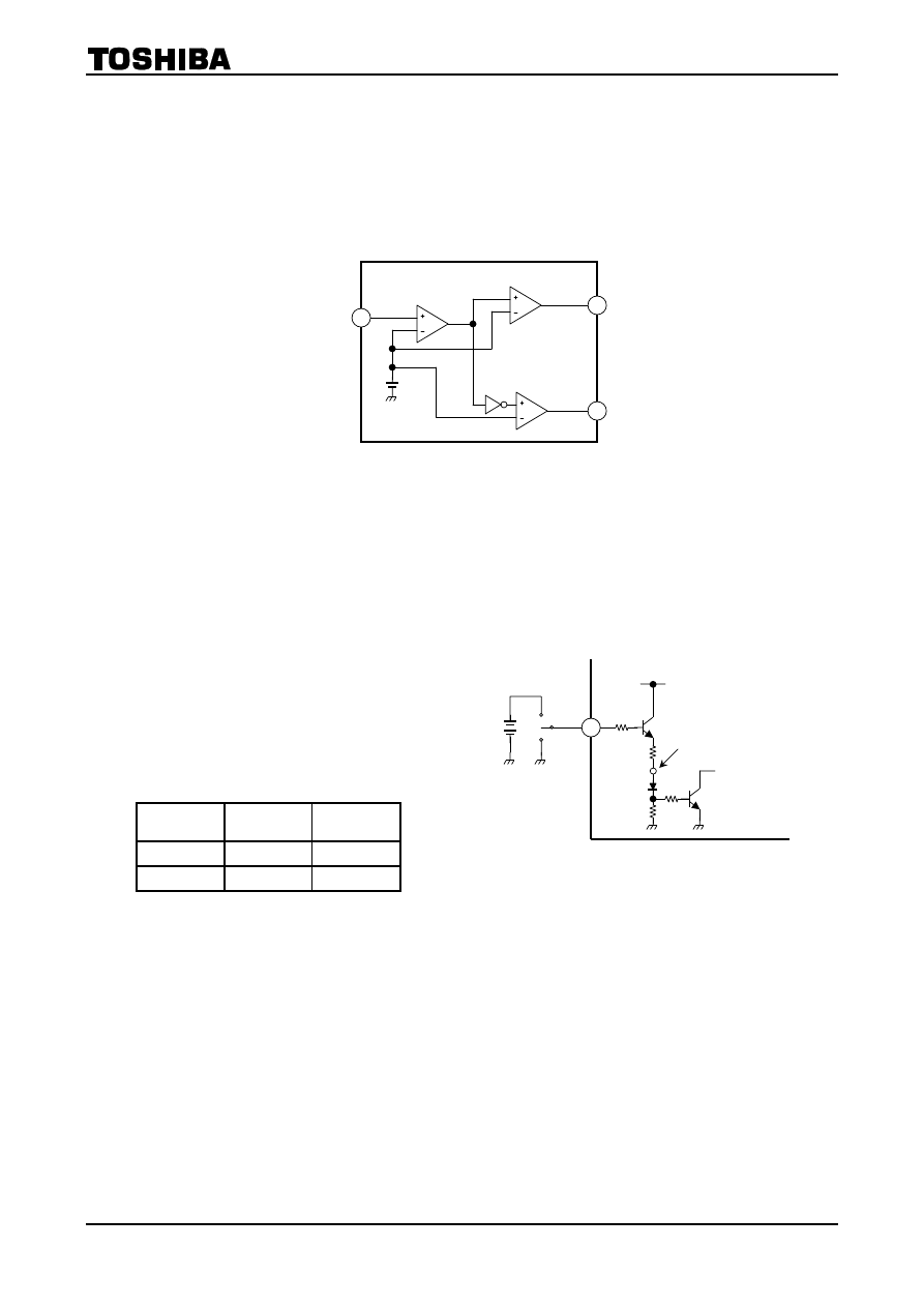
2. Stand-by SW Function
(pin 4)
By means of controlling pin 4 (stand-by terminal) to
high and low, the power supply can be set to ON and
OFF. The threshold voltage of pin 4 is set at about
3V
BE
(typ.), and the power supply current is about 2
mA (typ.) at the stand-by state.
Control Voltage of pin 4: V
SB
Stand-by Power V
SB
(V)
ON OFF
0~1.5
OFF ON
3~V
CC
Adjustage of Stand-by SW
(1) Since
V
CC
can directly be controlled to ON or OFF by the microcomputer, the switching relay can be
omitted.
(2) Since the control current is microscopic, the switching relay of small current capacity is satisfactory
for switching
Amp. 1
Input
Amp. 2A
Amp. 2B
Figure 1 Block Diagram
Figure 2 With pin 4 set to High,
Power is turned ON
ON
4
OFF
10 k
W
to BIAS
CUTTING CIRCUIT
» 2V
BE
V
CC
Power
TA8264AH
2002-02-13
4
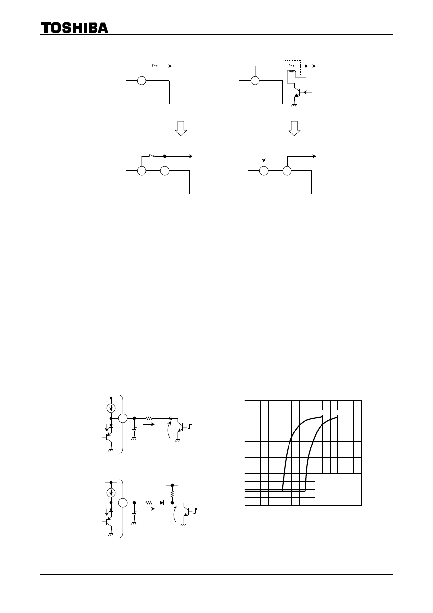
3. Muting
Function
(pin 22)
By means of controlling pin 22 less than 0.5 V, it can make the audio muting condition.
The muting time constant is decided by R
1
and C
4
and these parts is related the pop noise at power
ON/OFF.
The series resistance; R1 must be set up less than 10 kW to get enough muting attenuation.
The muting function have to be controlled by a transistor, FET and micro-controller port which has
I
MUTE
> 250 mA ability.
Pin 22 terminal voltage has the temperature characteristics of 4.6 V (low temperature) to 3.2 V (high
temperature).
Therefore, it is need to design with attention as using the micro-controller of which operating voltage is
less than 5 V.
Terminal 22 may not be pulled up and shall be controlled by OPEN/LOW.
When it is obliged to do, it must be pulled up via diode, because it has to defend flowing reverse current
to internal circuit of pin 22.
V
CC
Small current capacity switch
BATTERY
Stand-By
V
CC
DIRECTLY FROM
MICROCOMPUTER
BATTERY
Stand-By
– Stand-by Switch Method –
Figure 3
– Conventional Method –
V
CC
Large current capacity switch
BATTERY
V
CC
FROM
MICROCOMPUTER
BATTERY
RELAY
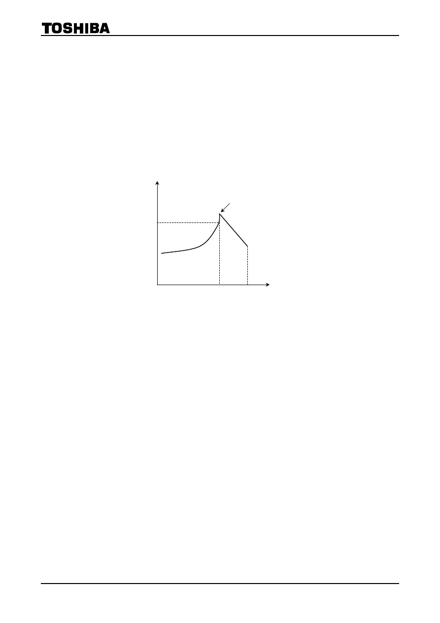
Figure 5 Mute Attenuation
---- V
MUTE
(V)
Point A voltage: VMUTE (V)
ATT – V
MUTE
Mut
e
a
tte
nu
ati
o
n A
T
T
(dB
)
10 k
W
5 k
W
VCC = 13.2 V
Po = 10 W
PL
= 4 W
f
= 1 kHz
-100
0
0.4
0.8 1 1.2
1.6 2 2.4 2.8
3
-80
-60
-40
-20
0
20
Figure 4 Muting Function
R
1
I (100
mA)
22
I
MUTE
I
MUTE (OFF)
A
V
MUTE
C
4
<Recommended Application>
<Application for pulled up>
R
1
I (100
mA)
22
I
MUTE
I
MUTE (OFF)
V
MUTE
C
4
TA8264AH
2002-02-13
5
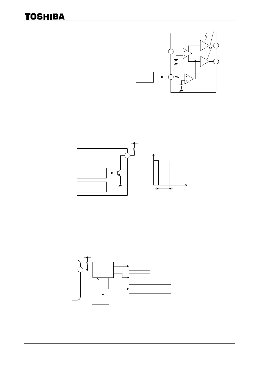
4. AUX
Input
(pin 16)
The pin 16 is for input terminal of AUX
amplifier.
The total gain is 0dB by using of AUX amplifier.
Therefore, the m-COM can directly drive the
AUX amplifier.
BEEP sound or voice synthesizer signal can be
input to pin 16 directly.
When AUX function is not used, this pin must be
connected to PRE-GND (pin 13) via a capacitor.
5.
Diagnosis Output
(pin 25)
This diagnosis output terminal of pin 25 has open collector output structure on chip as shown in Figure 7.
In case diagnosis circuit that detect unusual case is operated, NPN transistor (Q1) is turned on.
It is possible to protect all the system of apparatus as well as power IC protection.
In case of being unused this function, use this IC as open-connection on pin 25.
5.1
In Case of Shorting Output to V
CC
/GND or Over Voltage Power Supplied
NPN transistor (Q1) is turned on.
Threshold of over voltage protection: V
CC
= 22 V (typ.)
5.2
In Case of Shorting Output to Output
NPN transistor (Q1) is turned on and off in response to the input signal voltage.
25
5 V
LED/LCD
ALARM
REGULATOR → OFF
(Flashing)
(Announcement from a speaker.)
(Relay → OFF)
m-COM
MEMORY (Count and record)
Figure 8 Application 1
Figure 6 AUX Input
20dB AMP.
IN
OUT (
+)
OUT (
-)
16
AUX-IN
-
20dB
AUX AMP
m-COM
Figure 7 Self Diagnosis Output
pin 25: Open collector output (active low)
OUTPUT SHORT
PROTECTOR
OVER VOLTAGE
PROTECTOR
25
Q1
5 V
Q1 is turned on
GND
5 V
t
TA8264AH
2002-02-13
6
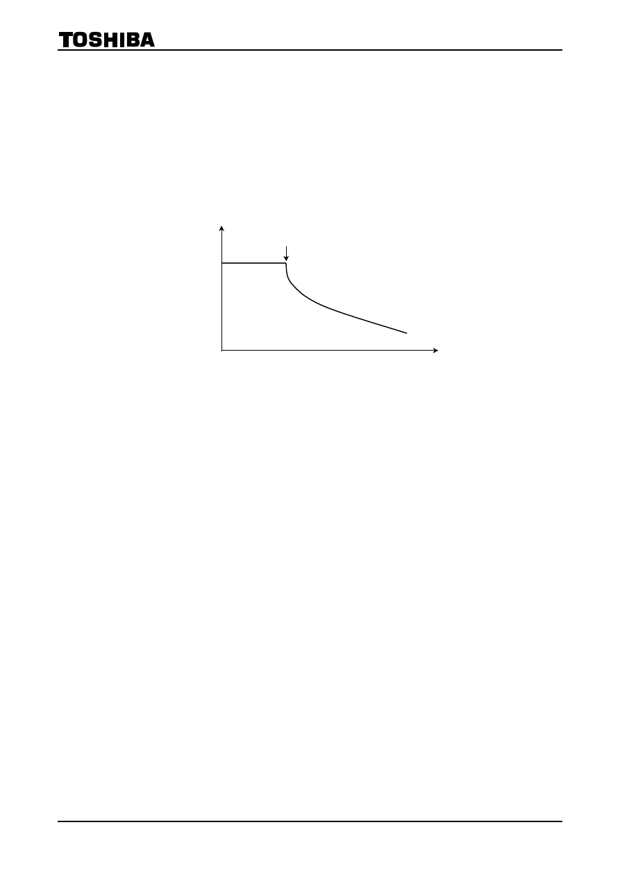
6. Prevention of speaker burning accident
(In Case of Rare Short Circuit of Speaker)
When the direct current resistance between OUT + and OUT - terminal becomes 1 W or less and output
current over 4 A flows, this IC makes a protection circuit operate and suppresses the current into a speaker.
This system makes the burning accident of the speaker prevent as below mechanism.
<The guess mechanism of a burning accident of the speaker>
Abnormal output offset voltage (voltage between OUT + and OUT -) over 4 V is made by the external
circuit failure.(Note 1)
¯
The speaker impedance becomes 1 W or less as it is in a rare short circuit condition.
¯
The current more than 4 A flows into the speaker and the speaker is burned.
Note 1: It is appeared by biased input DC voltage
(for example, large leakage of the input capacitor, short-circuit between copper patterns of PCB.)
Current into a speaker
Speaker impedance
Less than 4
W
Figure 9
About 1
W
4
W
Operating point of protector
TA8264AH
2002-02-13
7
6.1 Applications
When output terminals short-circuit to V
CC
or GND, the voltage of 25pin is fixed to “L”.
And when shorting OUT + to OUT -, “L” and “H” are switched according to an input signal.
Therefore, it is possible to judge how the power IC condition is if a micro-controller detects the
25pin voltage that is smoothed out with LPF.
It is recommend that the threshold voltage (Vth) is set up as higher as possible because output level
of LPF is changed according to an input signal.
(for example, Vth is set up to 4 V if 25pin is pulled up to 5 V line.)
Output voltage of L.P.F.
Output power
5 V
Figure 10
Operating point of protector
TA8264AH
2002-02-13
8
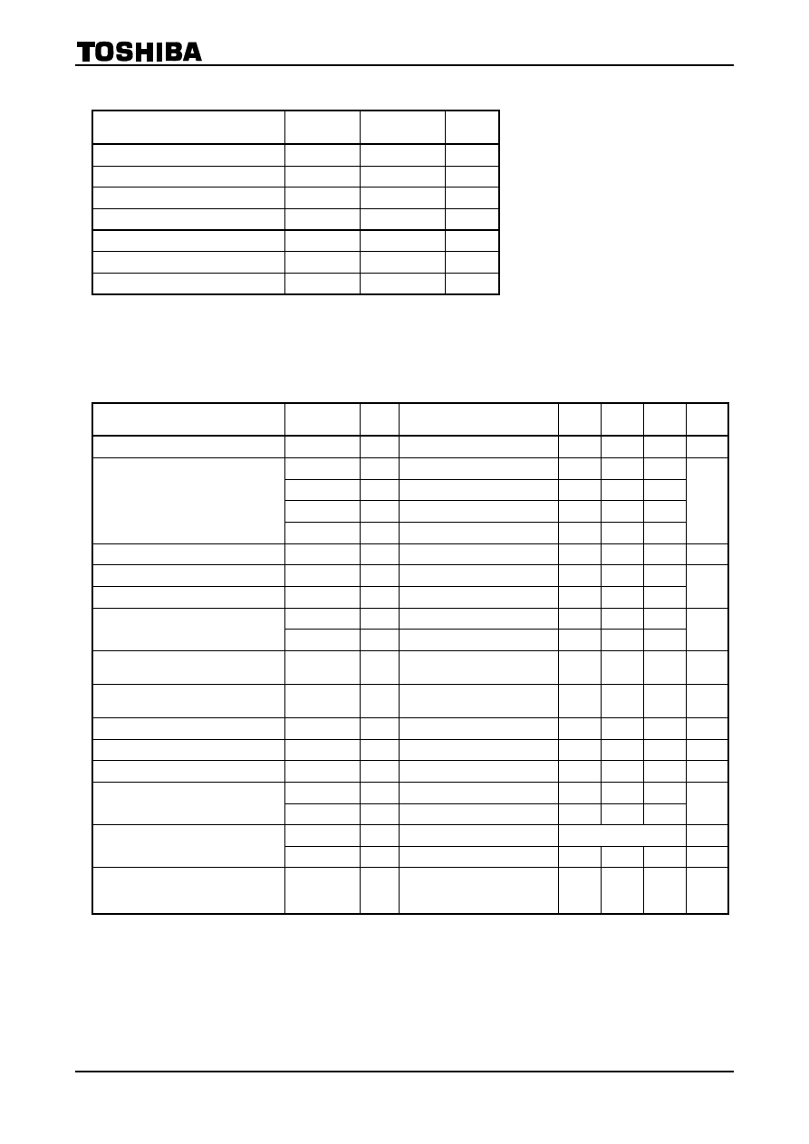
Maximum Ratings
(Ta
==== 25°C)
Characteristics Symbol
Rating
Unit
Peak supply voltage (0.2 s)
V
CC (surge)
50 V
DC supply voltage
V
CC (DC)
25 V
Operation supply voltage
V
CC (opr)
18 V
Output current (peak)
I
O (peak)
9 A
Power dissipation
P
D
(Note 2)
125
W
Operation temperature
T
opr
-40~85 °C
Storage temperature
T
stg
-55~150 °C
Note 2: Package thermal resistance
q
j-T
= 1°C/W (typ.)
(Ta
= 25°C, with infinite heat sink)
Electrical Characteristics
(unless otherwise specified V
CC
==== 13.2 V, f ==== 1 kHz, R
L
==== 4
9
9
9
9
, Ta
==== 25°C)
Characteristics Symbol
Test
Circuit
Test Condition
Min
Typ.
Max
Unit
Quiescent current
I
CCQ
¾
V
IN
= 0
¾ 200 400
mA
P
OUT
MAX (1)
¾
V
CC
= 14.4 V, max Power
¾ 41 ¾
P
OUT
MAX (2)
¾
V
CC
= 13.7 V, max Power
¾ 37 ¾
P
OUT
(1)
¾
V
CC
= 14.4 V, THD = 10%
¾ 24 ¾
Output power
P
OUT
(2)
¾ THD
= 10%
19
21
¾
W
Total harmonic distortion
THD
¾
P
OUT
= 5 W
¾ 0.02 0.2 %
Voltage gain
G
V
¾
V
OUT
= 0.775 Vrms (0dBm)
32
34
36
Voltage gain ratio
DG
V
¾
V
OUT
= 0.775 Vrms (0dBm)
-1.0 0 1.0
dB
V
NO
(1)
¾ Rg
= 0 W, DIN45405
¾ 0.20 ¾
Output noise voltage
V
NO
(2)
¾ Rg
= 0 W, BW = 20 Hz~20 kHz
¾ 0.18 0.42
mVrms
Ripple rejection ratio
R.R.
¾
f
rip
= 100 Hz, Rg = 620 W
V
rip
= 0.775 Vrms (0dBm)
40 50
¾ dB
Cross talk
C.T.
¾
Rg
= 620 W
V
OUT
= 0.775 Vrms (0dBm)
¾ 60 ¾ dB
Output offset voltage
V
OFFSET
¾
¾
-150 0 +150
mV
Input resistance
R
IN
¾
¾
¾ 30 ¾
k
W
Stand-by current
I
SB
¾ Stand-by
condition
¾ 2 10 mA
V
SB
H
¾ Power:
ON
3.0
¾
V
CC
Stand-by control voltage
V
SB
L
¾ Power:
OFF
0
¾ 1.5
V
V
M
H
¾ Mute:
OFF
Open
¾
Mute control voltage
(Note 3)
V
M
L
¾
Mute: ON, R
1
= 10 kW 0
¾ 0.5 V
Mute attenuation
ATT M
¾
Mute: ON,
V
OUT
= 7.75 Vrms (20dBm) at
Mute:
OFF.
80 90
¾ dB
Note 3: Muting function have to be controlled by open and low logic, which logic is a transistor, FET and
m-COM port
of I
MUTE
> 250
m
A ability.
This means than the mute control terminal : pin 22 must not be pulled-up.
TA8264AH
2002-02-13
9
Test Circuit
R
L
R
L
R
L
11
9
8
7
5
2
3
17
18
19
21
24
23
12
15
14
1
20
6
R
L
IN1
IN2
IN3
IN4
13
C
1
C
1
C
1
C
1
PRE-GND
10
25
4
22
OUT1 (
+)
PW-GND1
OUT1 (
-)
OUT2 (
+)
PW-GND2
OUT2 (
-)
OUT3 (
+)
PW-GND3
OUT3 (
-)
OUT4 (
+)
PW-GND4
OUT4 (
-)
TAB
V
CC1
V
CC2
C
3
R
1
C
4
1
m
F
C
2
: PRE-GND
: PW-GND
STBY
DIAGNOSIS
OUT
RIP MUTE
3900
m
F
0.22
mF
0.22
mF
0.22
mF
10
m
F
10 k
W
C
5
0.
1
m
F
0.22
mF
AUX IN
16
0.22
mF
C
6
TA8264AH
2002-02-13
10
Qui
e
s
c
en
t
cu
rr
ent
I
CCQ
(m
A
)
Output power P
OUT
(W)
T.H.D – P
OUT
T
o
ta
l
ha
rm
oni
c
di
st
or
ti
on
T
.H
.D
(%
)
Power supply voltage VCC (V)
I
CCQ
– V
CC
Frequency f (Hz)
T.H.D – f
T
o
ta
l
ha
rm
oni
c
di
st
or
ti
on
T
.H
.D
(%
)
Output power P
OUT
(W)
T.H.D – P
OUT
T
o
ta
l
ha
rm
oni
c
di
st
or
ti
on
T
.H
.D
(%
)
10
0
30
0
400
20
100
200
300
RL = ¥
VIN = 0
100
10
100 k
0.001
1
1 k
0.01
0.1
10 k
OUT2, 3
VCC = 13.2 V
RL = 4 W
Pout = 5 W
OUT3
OUT4
0.1
100
0.01
1
0.1
f
= 1 kHz
RL = 4 W
1
10
10
100
13.2 V
16.0 V
9.0 V
0.1
100
0.01
1
0.1
VCC = 13.2 V
RL = 4 W
1
10
10
100
10 kHz
1 kHz
100 Hz
TA8264AH
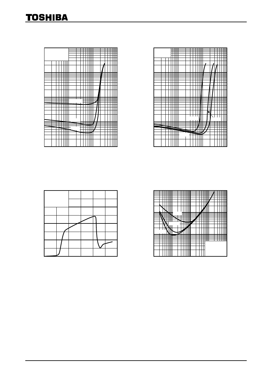
2002-02-13
11
Cr
o
s
s
t
a
lk
C.T
. (
d
B)
Cr
o
s
s
t
a
lk
C.T
. (
d
B)
Singnal source resistance Rg (9)
V
NO
– R
g
Outp
ut noi
s
e
v
o
lt
a
ge
V
NO
(m
V
rms
)
Frequency f (Hz)
R.R. – f
R
ippl
e
rej
e
cti
on
rati
o R
.R
. (
d
B
)
Frequency f (Hz)
C.T. – f (OUT1)
Cr
o
s
s
t
a
lk
C.T
. (
d
B)
Frequency f (Hz)
C.T. – f (OUT2)
Frequency f (Hz)
C.T. – f (OUT3)
Frequency f (Hz)
C.T. – f (OUT4)
Cr
o
s
s
t
a
lk
C.T
. (
d
B)
100
10
100 k
-70
0
1 k
-60
-30
10 k
-40
-20
-50
-10
VCC = 13.2 V
RL = 4 W
Rg = 620 W
Vrip = 0dBm
100
10
100 k
-70
0
1 k
-60
-30
10 k
-40
-20
-50
-10
VCC = 13.2 V
RL = 4 W
VOUT = 0dBm
Rg = 620 W
OUT1
® OUT2, 3, 4
100
10
100 k
-70
0
1 k
-60
-30
10 k
-40
-20
-50
-10
OUT2
® OUT1, 3, 4
VCC = 13.2 V
RL = 4 W
VOUT = 0dBm
Rg = 620 W
100
10
100 k
-70
0
1 k
-60
-30
10 k
-40
-20
-50
-10
OUT3
® OUT4
OUT3
® OUT1, 2
VCC = 13.2 V
RL = 4 W
VOUT = 0dBm
Rg = 620 W
100
10
100 k
1 k
10 k
-70
0
-60
-30
-40
-20
-50
-10
OUT4
® OUT1, 2, 3
VCC = 13.2 V
RL = 4 W
VOUT = 0dBm
Rg = 620 W
100
10
100 k
0
300
1 k
50
200
10 k
100
150
250
VCC = 13.2 V
RL = 4 W
BW
= 20 Hz~20 kHz
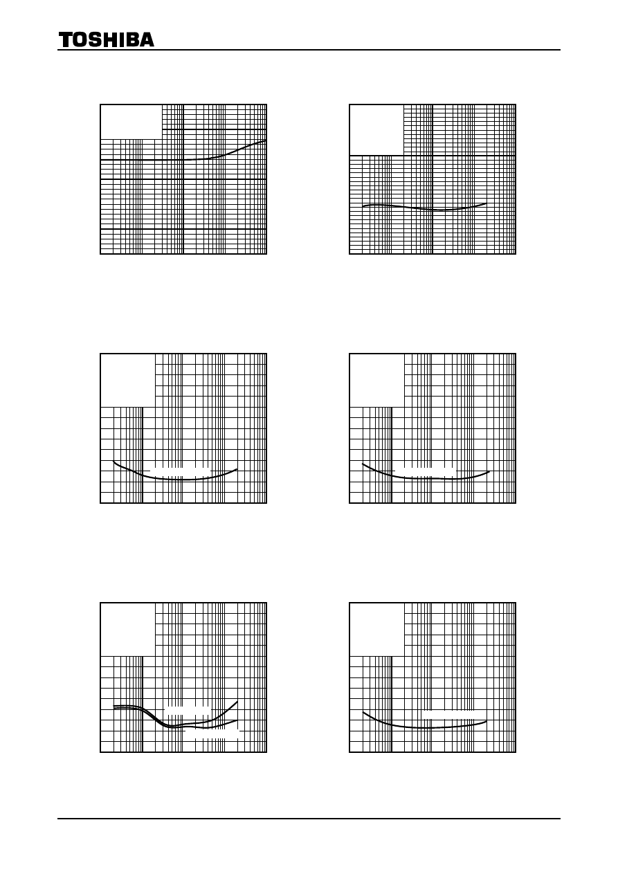
TA8264AH
2002-02-13
12
Frequency f (Hz)
G
V
– f
V
o
lt
ag
e g
a
in
G
V
(dB
)
Output power P
OUT
/ch (C)
P
D
– POUT
P
o
w
e
r di
ssi
p
a
ti
on
P
D
(
W
)
Ambient temperature Ta (°C)
P
D
MAX – Ta
A
llo
w
abl
e p
o
w
e
r di
s
s
ipati
o
n
P
D
MA
X
(W
)
①
②
③
25
0
150
0
120
75
60
100
40
20
80
100
50 125
① INFINITE HEAT SINK
R
qJC = 1°C/W
② HEAT SINK (R
qHS = 3.5°C/W)
R
qJC + RqHS = 4.5°C/W
③ NO HEAT SINK
R
qJA = 39°C/W
100
10
100 k
0
40
1 k
5
20
10 k
15
25
10
30
35
VCC = 13.2 V
RL = 4 W
VOUT = 0dBm
0
10
40
30
50
20
60
70
5
15 20
10
25
0
9 V
13.2 V
16 V
f
= 1 kHz
RL = 4 W
TA8264AH
2002-02-13
13
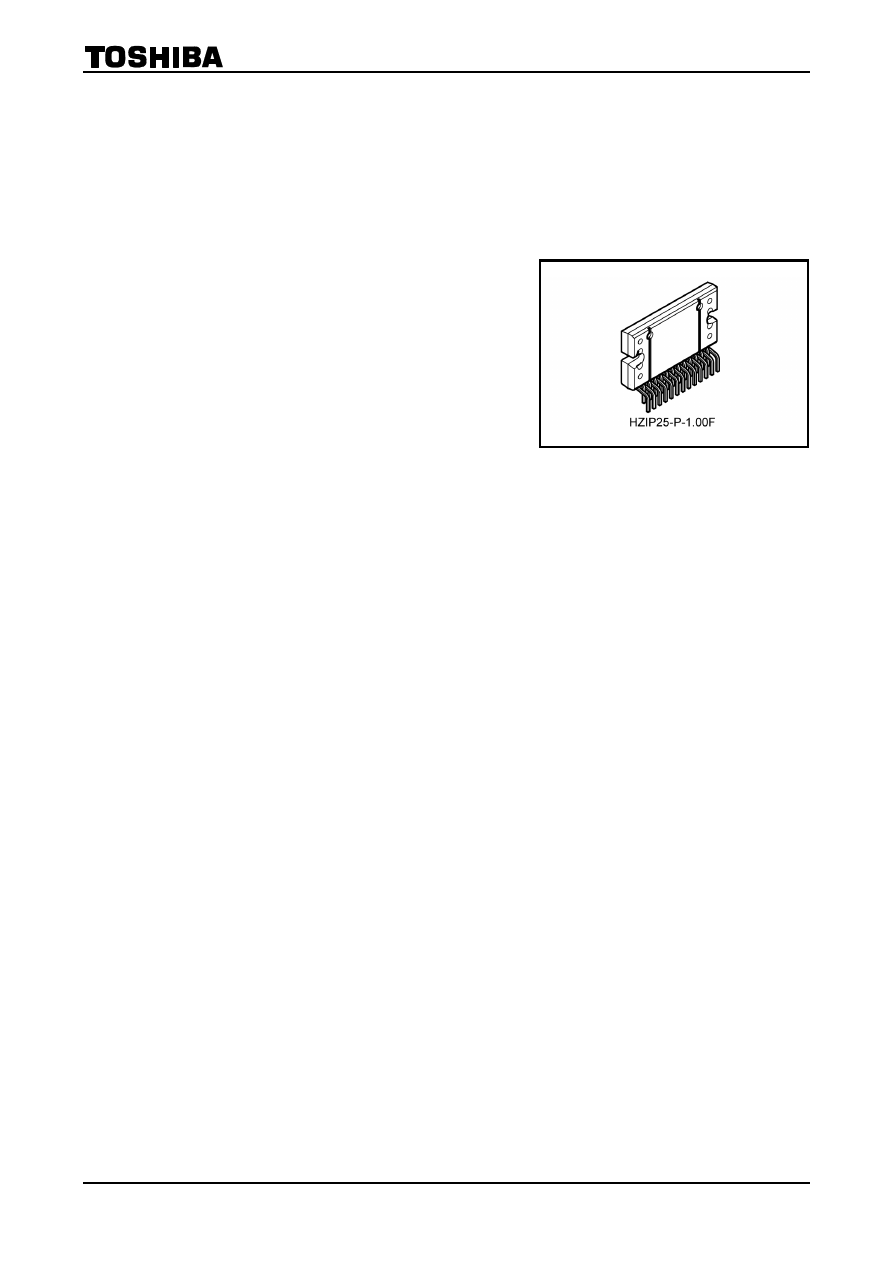
Package Dimensions
Weight: 7.7 g (typ.)

TA8264AH
2002-02-13
14
· TOSHIBA is continually working to improve the quality and reliability of its products. Nevertheless, semiconductor
devices in general can malfunction or fail due to their inherent electrical sensitivity and vulnerability to physical
stress. It is the responsibility of the buyer, when utilizing TOSHIBA products, to comply with the standards of
safety in making a safe design for the entire system, and to avoid situations in which a malfunction or failure of
such TOSHIBA products could cause loss of human life, bodily injury or damage to property.
In developing your designs, please ensure that TOSHIBA products are used within specified operating ranges as
set forth in the most recent TOSHIBA products specifications. Also, please keep in mind the precautions and
conditions set forth in the “Handling Guide for Semiconductor Devices,” or “TOSHIBA Semiconductor Reliability
Handbook” etc..
· The TOSHIBA products listed in this document are intended for usage in general electronics applications
(computer, personal equipment, office equipment, measuring equipment, industrial robotics, domestic appliances,
etc.). These TOSHIBA products are neither intended nor warranted for usage in equipment that requires
extraordinarily high quality and/or reliability or a malfunction or failure of which may cause loss of human life or
bodily injury (“Unintended Usage”). Unintended Usage include atomic energy control instruments, airplane or
spaceship instruments, transportation instruments, traffic signal instruments, combustion control instruments,
medical instruments, all types of safety devices, etc.. Unintended Usage of TOSHIBA products listed in this
document shall be made at the customer’s own risk.
· This product generates heat during normal operation. However, substandard performance or malfunction may
cause the product and its peripherals to reach abnormally high temperatures.
The product is often the final stage (the external output stage) of a circuit. Substandard performance or
malfunction of the destination device to which the circuit supplies output may cause damage to the circuit or to the
product.
· The products described in this document are subject to the foreign exchange and foreign trade laws.
· The information contained herein is presented only as a guide for the applications of our products. No
responsibility is assumed by TOSHIBA CORPORATION for any infringements of intellectual property or other
rights of the third parties which may result from its use. No license is granted by implication or otherwise under
any intellectual property or other rights of TOSHIBA CORPORATION or others.
· The information contained herein is subject to change without notice.
000707EBF
RESTRICTIONS ON PRODUCT USE

This datasheet has been download from:
Datasheets for electronics components.
Wyszukiwarka
Podobne podstrony:
Horiz deflect tranz toshiba
Toshiba Satellite Pro`50
Enter Service Toshiba
więcej podobnych podstron