
MODBUS over serial line specification and implementation guide V1.02
Modbus-IDA.ORG
Modbus.org
http://www.modbus.org/
1/44
Dec 20, 2006
MODBUS over Serial Line
Specification and Implementation Guide
V1.02

MODBUS over serial line specification and implementation guide V1.02
Modbus-IDA.ORG
Modbus.org http://www.modbus.org/ 2/44
Dec 20, 2006
Contents
1 Introduction .............................................................................. 4
Scope of this document ............................................................. 4
overview....................................................................... 5
1.3 Conventions ............................................................................... 5
1.4 Compliance ................................................................................ 6
1.5 Glossary..................................................................................... 6
2
MODBUS Data Link Layer ....................................................... 7
MODBUS Master / Slaves protocol principle.............................. 7
MODBUS Addressing rules........................................................ 8
MODBUS frame description....................................................... 8
Master / Slaves State Diagrams................................................. 9
The two serial Transmission Modes......................................... 12
Error Checking Methods .......................................................... 19
Layer........................................................................ 20
Data Signaling Rates ............................................................... 20
Interfaces.................................................................. 21
Multipoint System requirements............................................... 27
Interfaces .............................................................. 29
3.6 Cables...................................................................................... 32
3.7 Visual
Diagnosis ...................................................................... 32
4
Installation and Documentation ............................................. 33
Guide ............................................................................... 33
5 Implementation
Classes ........................................................ 34
6 Appendix ................................................................................ 35
Appendix A - Management of Serial Line Diagnostic Counters 35
Appendix B - LRC/CRC Generation ......................................... 38
Appendix E - References ......................................................... 44

MODBUS over serial line specification and implementation guide V1.02
Modbus-IDA.ORG
Modbus.org
http://www.modbus.org/
3/44
Dec 20, 2006
Document modifications
Month-Year
Modifications
1.0
Nov 02
Creation.
This document comprises a description of Master / slave protocol and of the two
different transmission modes ( RTU, ASCII).
The main features of the physical layer ( RS485, RS232) and some recommendations
are provided.
Implementation classes are proposed to guide the implementation.
1.01 Aug 30, 2006 Minor clarifications and correction of typos.
1.02 Dec 20, 2006 Minor clarifications and correction of typos.
MODBUS over serial line specification and implementation guide V1.02
Modbus-IDA.ORG
Modbus.org http://www.modbus.org/ 4/44
Dec 20, 2006
1 Introduction
1.1
Scope of this document
The MODBUS standard defines an application layer messaging protocol, positioned at level 7 of the OSI model that provides
"client/server" communications between devices connected on different types of buses or networks. It standardizes also a specific
protocol on serial line to exchange MODBUS request between a master and one or several slaves.
The objective of this document is to present the MODBUS protocol over serial line, in order to be used by all system designers when
they want to implement MODBUS protocol on their serial line products. Thus, this document will facilitate interoperability between
devices using the MODBUS protocol.
This document comes in complement to the document called "MODBUS Application Protocol Specification".
In chapter 5 different implementation classes are defined for "MODBUS Serial Line". Specification of a class is the sum of
requirements that a device must respect in order to belong to that class.
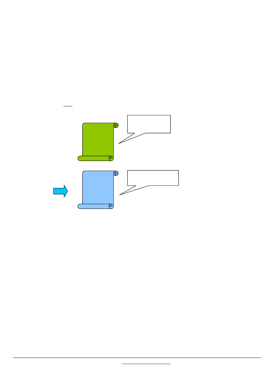
Figure 1:
General overview of MODBUS documents
MODBUS
Application
Protocol
Specification
The MODBUS
application protocol
(
OSI Level 7)
MODBUS over
Serial Line
Specification &
Implementation
Guide
Serial Line specification
(OSI Levels 1 & 2)
This
document
MODBUS over serial line specification and implementation guide V1.02
Modbus-IDA.ORG
Modbus.org
http://www.modbus.org/
5/44
Dec 20, 2006
1.2 Protocol
overview
This document describes the MODBUS over Serial Line protocol. MODBUS Serial Line protocol is a Master-Slave protocol. This
protocol takes place at level 2 of the OSI model.
A master-slave type system has one node (the master node) that issues explicit commands to one of the "slave" nodes and processes
responses. Slave nodes will not typically transmit data without a request from the master node, and do not communicate with other
slaves.
At the physical level, MODBUS over Serial Line systems may use different physical interfaces (RS485, RS232). TIA/EIA-485 (RS485)
Two-Wire interface is the most common. As an add-on option, RS485 Four-Wire interface may also be implemented. A TIA/EIA-232-
E (RS232) serial interface may also be used as an interface, when only short point to point communication is required. (see chapter
"Physical Layer")
The following figure gives a general representation of MODBUS serial communication stack compared to the 7 layers of the OSI
model.
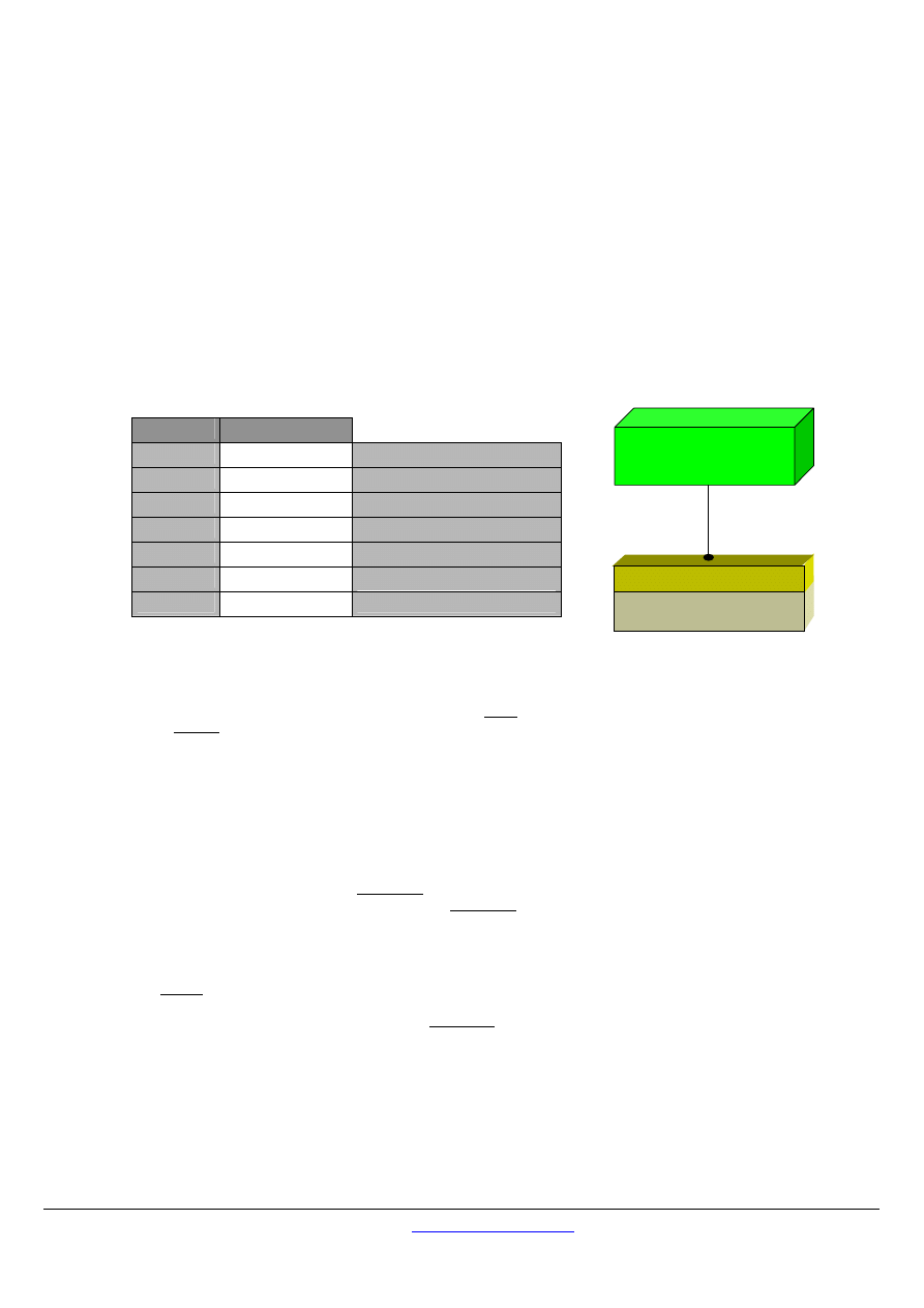
Layer
ISO/OSI Model
7
Application
MODBUS Application Protocol
6
Presentation
Empty
5
Session
Empty
4
Transport
Empty
3
Network
Empty
2
Data Link
MODBUS Serial Line Protocol
1
Physical
EIA/TIA-485
(or EIA/TIA-232)
Figure 2:
MODBUS Protocols and ISO/OSI Model
MODBUS application layer messaging protocol, positioned at level 7 of the OSI model, provides client/server communication between
devices connected on buses or networks. On MODBUS serial line the client role is provided by the Master of the serial bus and the
Slaves nodes act as servers.
1.3 Conventions
In this document, the following words are used to define the significance of each particular requirement.
"MUST" / "REQUIRED"
All requirements containing the word "MUST" are mandatory. The word MUST, or the adjective "REQUIRED", means that the item is
an absolute requirement of the implementation. These words are
underlined
.
"SHOULD" / "RECOMMENDED"
All recommendations containing the word "SHOULD", or the adjective “RECOMMENDED”, are considered desired behavior. These
recommendations should be used as a guideline when choosing between different options to implement functionality. There may be
valid reasons in particular circumstances to ignore this item, but the full implications should be understood and the case carefully
weighed before choosing a different course. These words are
underlined
.
"MAY" / "OPTIONAL"
The word “MAY”, or the adjective "OPTIONAL", means that this item is truly optional. One designer may choose to include the item
because a particular marketplace requires it or because it enhances the product, for example; another designer may omit the same
item.
EIA/TIA-485
(or EIA/TIA-232)
MODBUS Master / Slave
MODBUS Application
Layer
Client / server

MODBUS over serial line specification and implementation guide V1.02
Modbus-IDA.ORG
Modbus.org http://www.modbus.org/ 6/44
Dec 20, 2006
1.4 Compliance
An implementation is not in conformity if it fails to satisfy one or more of the MUST requirements from its implementation class.
An implementation that satisfies all the MUST requirements and all the SHOULD recommendations is said to be "unconditionally
compliant".
One that satisfies all the MUST requirements but not all the SHOULD recommendations is said to be "conditionally compliant".
1.5 Glossary
Definition of particular words, symbols, and abbreviations used in this document.
2W
The Two-Wire configuration defined in the “Electrical Interface” chapter, or one of its interfaces.
4W
The Four-Wire configuration defined in the “Electrical Interface” chapter, or one of its interfaces.
AUI
Attachment Unit Interface
AWG American Wire Gauge, a standard method denoting wire diameter; please see Appendix E - References.
Common
The Signal Common in EIA/TIA Standards. In a 2W-or 4W-RS485 MODBUS Network, Signal and optional
Power Supply Common
DCE
a MODBUS Device, for example a programmable controller adapter, which implements an RS232 Data
Circuit-terminating Equipment, also named Data Communication Equipment.
Device
or “MODBUS device” : see this definition.
Driver
Generator, or Transmitter.
DTE
a MODBUS Device, for example a programming panel or a PC, which implements an RS232 Data
Terminal Equipment.
ITr
Physical bus Interface on Trunk side.
IDv
Physical bus Interface on Derivation (or tap or device drop) side.
LT Line
Termination.
MODBUS Device
a Device that implements MODBUS over Serial Line and respects this Technical Note.
RS232
EIA/ TIA -232 Standard.
RS485
EIA/ TIA -485 Standard.
RS485-MODBUS
A 2W-or 4W-Network in accordance with this Technical Note.
Transceiver a
Transmitter and a Receiver (or Driver and Receiver).
MODBUS over serial line specification and implementation guide V1.02
Modbus-IDA.ORG
Modbus.org
http://www.modbus.org/
7/44
Dec 20, 2006
2
MODBUS Data Link Layer
2.1
MODBUS Master / Slaves protocol principle
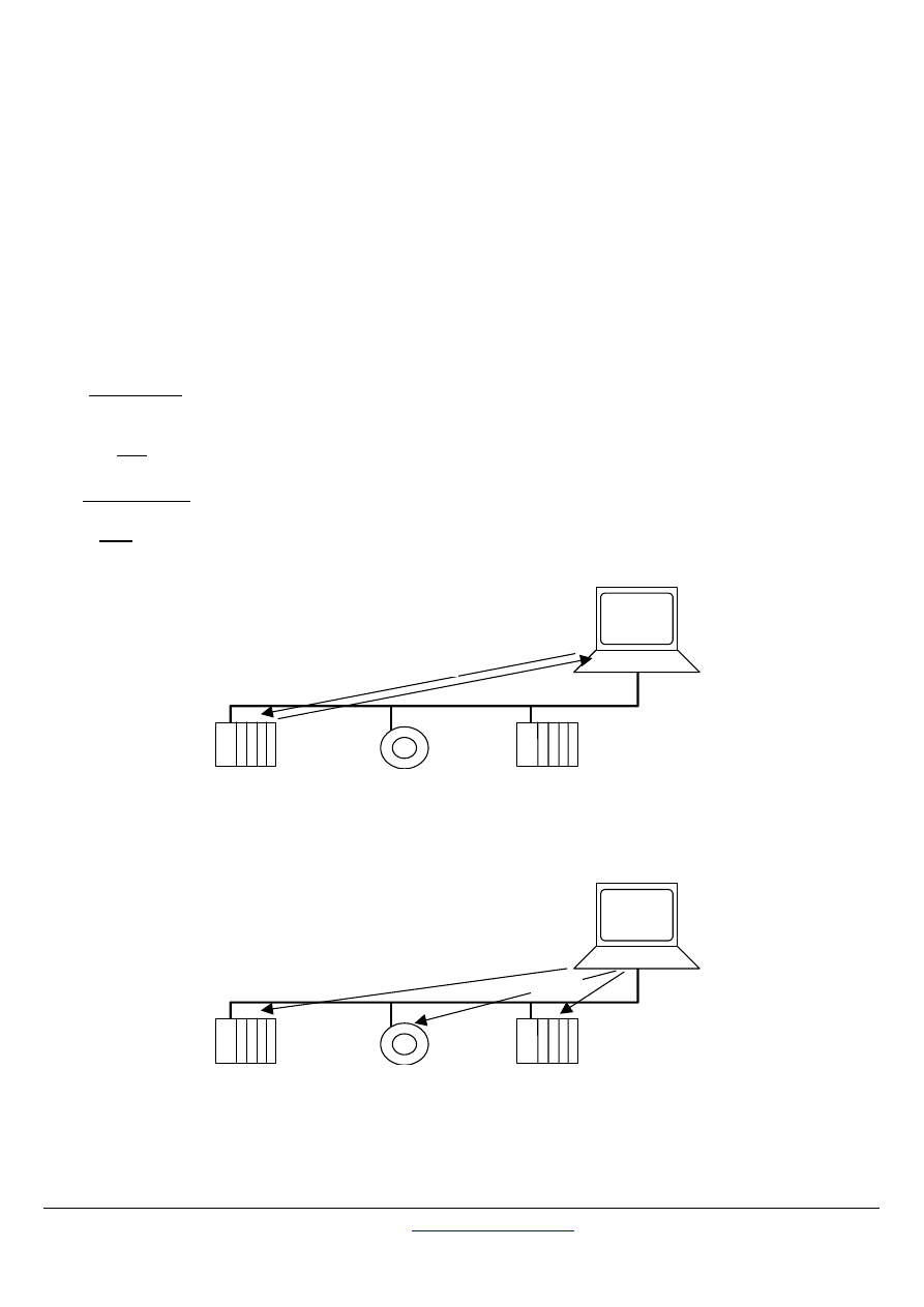
The MODBUS Serial Line protocol is a Master-Slaves protocol. Only one master (at the same time) is connected to the bus, and one
or several (247 maximum number) slaves nodes are also connected to the same serial bus. A MODBUS communication is always
initiated by the master. The slave nodes will never transmit data without receiving a request from the master node. The slave nodes
will never communicate with each other. The master node initiates only one MODBUS transaction at the same time.
The master node issues a MODBUS request to the slave nodes in two modes :
In unicast mode, the master addresses an individual slave. After receiving and processing the request, the slave returns a
message (a 'reply') to the master .
In that mode, a MODBUS transaction consists of 2 messages : a request from the master, and a reply from the slave.
Each slave must have an unique address (from 1 to 247) so that it can be addressed independently from other nodes.
In broadcast mode, the master can send a request to all slaves.
No response is returned to broadcast requests sent by the master. The broadcast requests are necessarily writing commands. All
devices must accept the broadcast for writing function. The address 0 is reserved to identify a broadcast exchange.
slave
slave
slave
master
request
reply
Figure 3:
Unicast mode
slave
slave
slave
master
request
Figure 4:
Broadcast mode
MODBUS over serial line specification and implementation guide V1.02
Modbus-IDA.ORG
Modbus.org http://www.modbus.org/ 8/44
Dec 20, 2006
2.2
MODBUS Addressing rules
The MODBUS addressing space comprises 256 different addresses.
0
From 1 to 247
From 248 to 255
Broadcast
address
Slave individual addresses
Reserved
The Address 0 is reserved as the broadcast address. All slave nodes must recognise the broadcast address.
The MODBUS Master node has no specific address, only the slave nodes must have an address. This address must be unique on a
MODBUS serial bus.
2.3
MODBUS frame description
The MODBUS application protocol [1] defines a simple Protocol Data Unit (PDU) independent of the underlying communication layers:
Function code
Data
MODBUS PDU
Figure 5:
MODBUS Protocol Data Unit
The mapping of MODBUS protocol on a specific bus or network introduces some additional fields on the Protocol Data Unit. The
client that initiates a MODBUS transaction builds the MODBUS PDU, and then adds fields in order to build the appropriate
communication PDU.
Address field
Function code
Data
CRC
(or LRC)
MODBUS SERIAL LINE PDU
MODBUS PDU
Figure 6:
MODBUS frame over Serial Line
On MODBUS Serial Line, the Address field only contains the slave address.
As described in the previous section the valid slave nodes addresses are in the range of 0 – 247 decimal. The individual slave
devices are assigned addresses in the range of 1 – 247. A master addresses a slave by placing the slave address in the address field
of the message. When the slave returns its response, it places its own address in the response address field to let the master know
which slave is responding.
The function code indicates to the server what kind of action to perform. The function code can be followed by a data field that
contains request and response parameters.
Error checking field is the result of a "Redundancy Checking" calculation that is performed on the message contents. Two kinds
of calculation methods are used depending on the transmission mode that is being used (RTU or ASCII). (see 2.5 section, "The
two serial Transmission Modes")
MODBUS over serial line specification and implementation guide V1.02
Modbus-IDA.ORG
Modbus.org
http://www.modbus.org/
9/44
Dec 20, 2006
2.4
Master / Slaves State Diagrams
The MODBUS data link layer comprises two separate sub layers :
•
The Master / slave protocol
•
The transmission mode ( RTU vs ASCII modes)
The following sections describes the state diagrams of a master and a slave that are independent of transmission modes used.
The RTU and ASCII transmission modes are specified in next chapters using two state diagrams. The reception and the sending of a
frame are described.
Syntax of state diagram :
The following state diagrams are drawn in compliance with UML standard notations. The notation is briefly recalled below :
State_B
trigger [ guard condition ]
/ action
State_A
When a "trigger" event occurs in a system being in "State_A", system is going into "State_B", only if "guard condition" is true. An action "action" is then
performed.
2.4.1
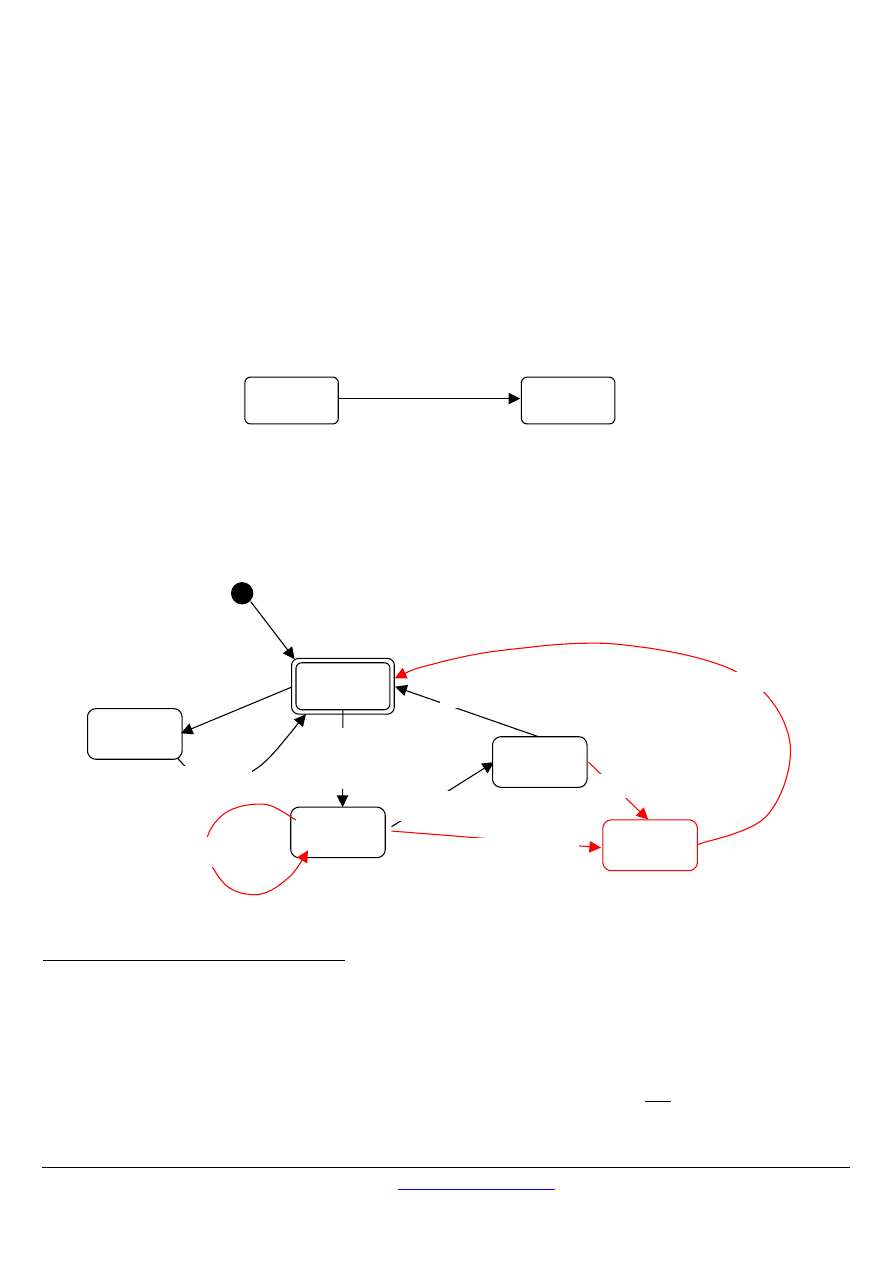
Master State diagram
The following drawing explains the Master behavior :
Waiting
for reply
Idle
request sent to a
slave
/ response time-
out is started
Processing
reply
Reply reception [Expected slave]
/ response time-out is stopped
End of reply processing
Processing
error
Frame error
response
time-out expiration
End of error processing
Waiting
turnaround
delay
Request sent in
broadcast mode
/ turnaround delay
is started
turnaround delay
expiration
Reply reception
[Unexpected slave]
Figure 7:
Master state diagram
Some explanations about the state diagram above :
State "Idle" = no pending request. This is the initial state after power-up. A request can only be sent in "Idle" state. After sending
a request, the Master leaves the "Idle" state, and cannot send a second request at the same time
When a unicast request is sent to a slave, the master goes into "Waiting for reply" state, and a “Response Time-out” is started. It
prevents the Master from staying indefinitely in "Waiting for reply" state. Value of the Response time-out is application
dependant.
When a reply is received, the Master checks the reply before starting the data processing. The checking may result in an error,
for example a reply from an unexpected slave, or an error in the received frame. In case of a reply received from an unexpected
slave, the Response time-out is kept running. In case of an error detected on the frame, a retry may be performed.
If no reply is received, the Response time-out expires, and an error is generated. Then the Master goes into "Idle" state, enabling
a retry of the request. The maximum number of retries depends on the master set-up.
MODBUS over serial line specification and implementation guide V1.02
Modbus-IDA.ORG
Modbus.org http://www.modbus.org/ 10/44
Dec 20, 2006
When a broadcast request is sent on the serial bus, no response is returned from the slaves. Nevertheless a delay is respected
by the Master in order to allow any slave to process the current request before sending a new one. This delay is called
"Turnaround delay". Therefore the master goes into "Waiting Turnaround delay" state before going back in "idle" state and before
being able to send another request.
In unicast the Response time out must be set long enough for any slave to process the request and return the response, in
broadcast the Turnaround delay must be long enough for any slave to process only the request and be able to receive a new one.
Therefore the Turnaround delay should be shorter than the Response time-out. Typically the Response time-out is from 1s to
several second at 9600 bps; and the Turnaround delay is from 100 ms to 200ms.
Frame error consists of : 1) Parity checking applied to each character; 2) Redundancy checking applied to the entire frame. See
§2.6 "Error Checking Methods" for more explanations.
The state diagram is intentionally very simple. It does not take into account access to the line, message framing, or retry following
transmission error, etc … For more details about frame transmission, please refer to 2.5 paragraph, "The two serial Transmission
Modes".
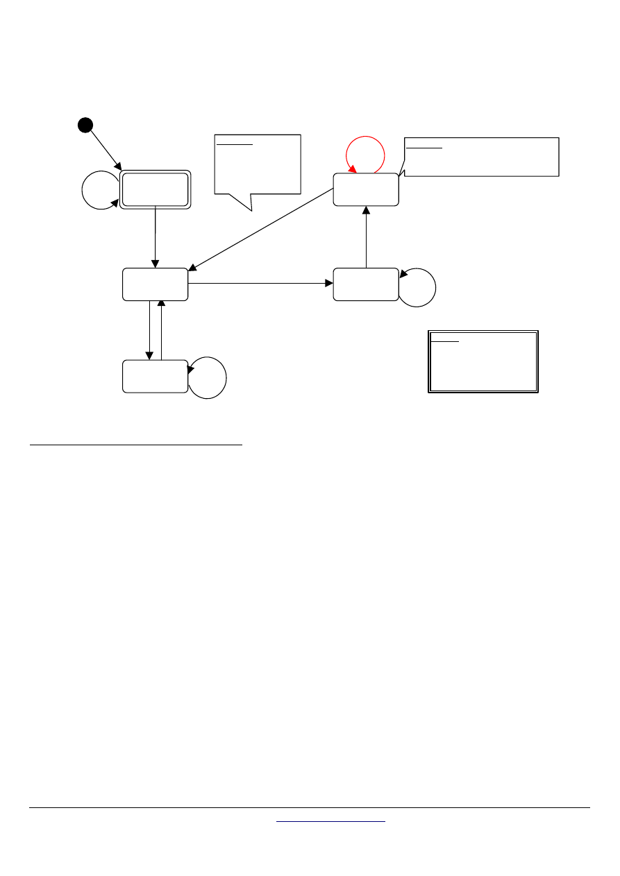
2.4.2
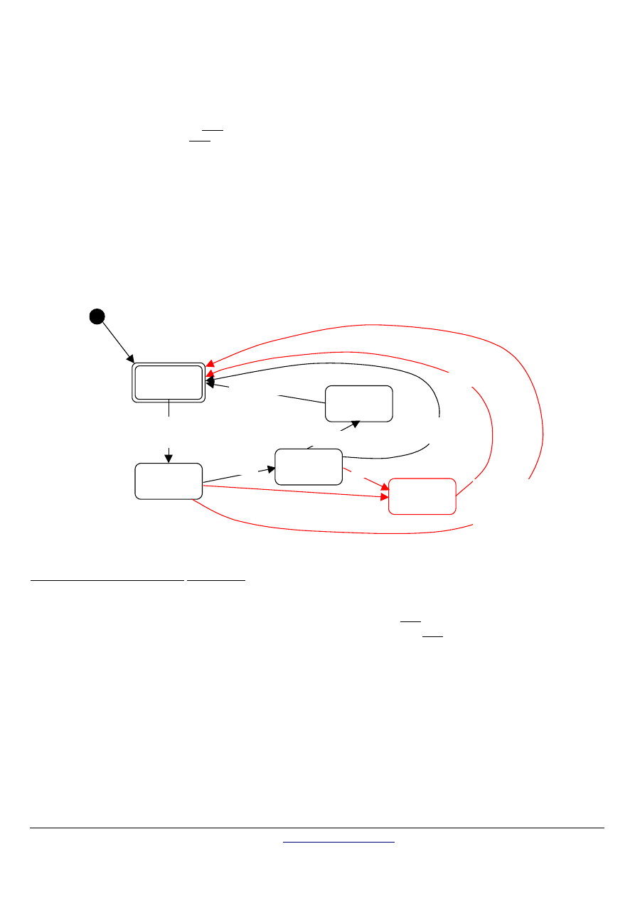
Slave State Diagram
The following drawing explains the Slave behavior :
Checking
request
Idle
Processing
required action
normal reply sent
Formatting
error reply
error while processing
error in request data
error reply sent
Formatting
normal reply
check OK
end of processing [unicast mode]
end of processing
[broadcast mode]
error in frame
checking, or
frame not
addressed to
this slave
reception of a
request
(from the master)
Figure 8:
Slave state diagram
Some explanations about the above state diagram :
State "Idle" = no pending request. This is the initial state after power-up.
When a request is received, the slave checks the packet before performing the action requested in the packet. Different errors
may occur : format error in the request, invalid action, … In case of error, a reply must be sent to the master.
Once the required action has been completed, a unicast message requires that a reply must be formatted and sent to the master.
If the slave detects an error in the received frame, no respond is returned to the master.
MODBUS diagnostics counters are defined and should be managed by any slave in order to provide diagnostic information.
These counters can be get using the Diagnostic MODBUS function (see Appendix A, and the MODBUS application protocol
specification [1]).
MODBUS over serial line specification and implementation guide V1.02
Modbus-IDA.ORG
Modbus.org
http://www.modbus.org/
11/44
Dec 20, 2006
2.4.3
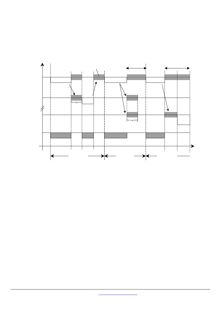
Master / Slave communication time diagram
This following figure shows the time diagram of 3 typical scenarios of Master / Slave communications.
REQUEST
Master
Reply analysis and
preparation of the
following exchange
Wait
Wait
Wait
Slave 1
Slave N
Physical
line
BROADCAST
REQUEST
REPLY
NO
REPLY
Exchange i-1
Exchange i
Exchange i+1
Time
Request
treatment
Simultaneous execution of
the order by the slaves
to slave 1
to slave N
Response time out
error
Error detection
Turnaround delay
Figure 9:
Master / Slave scenario time diagram
Remarks :
the duration of the REQUEST, REPLY, BROACAST phases depends on the communication features (frame length and
throughput).
the duration of the WAIT and TREATMENT phases depends on the request processing time needed for the slave application.

MODBUS over serial line specification and implementation guide V1.02
Modbus-IDA.ORG
Modbus.org http://www.modbus.org/ 12/44
Dec 20, 2006
2.5
The two serial Transmission Modes
Two different serial transmission modes are defined : The RTU mode and the ASCII mode.
It defines the bit contents of message fields transmitted serially on the line. It determines how information is packed into the message
fields and decoded.
The transmission mode (and serial port parameters) must be the same for all devices on a MODBUS Serial Line.
Although the ASCII mode is required in some specific applications, interoperability between MODBUS devices can be reached only if
each device has the same transmission mode : All devices must implement the RTU Mode. The ASCII transmission mode is an
option.
Devices should be set up by the users to the desired transmission mode, RTU or ASCII. Default setup must be the RTU mode.
2.5.1
RTU Transmission Mode
When devices communicate on a MODBUS serial line using the RTU (Remote Terminal Unit) mode, each 8–bit byte in a message
contains two 4–bit hexadecimal characters. The main advantage of this mode is that its greater character density allows better data
throughput than ASCII mode for the same baud rate. Each message must be transmitted in a continuous stream of characters.
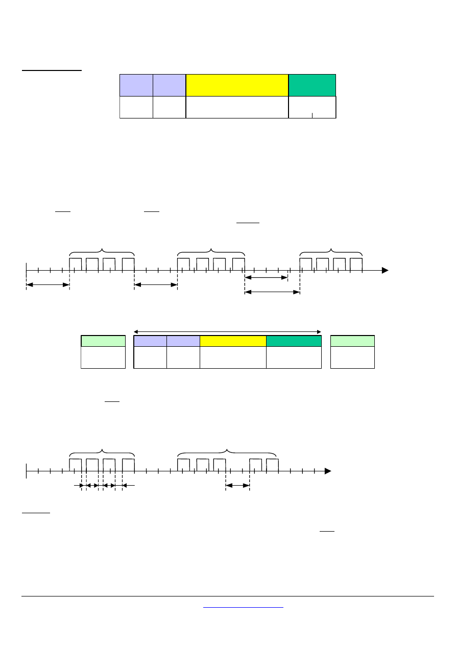
The format ( 11 bits ) for each byte in RTU mode is :
Coding System:
8–bit binary
Bits per Byte:
1 start bit
8 data bits, least significant bit sent first
1 bit for parity completion
1 stop bit
Even parity is required, other modes ( odd parity, no parity ) may also be used. In order to ensure a maximum compatibility with
other products, it is recommended to support also No parity mode. The default parity mode must be even parity.
Remark : the use of no parity requires 2 stop bits.
How Characters are Transmitted Serially :
Each character or byte is sent in this order (left to right):
Least Significant Bit (LSB) . . . Most Significant Bit (MSB)
Start
With Parity Checking
1
2
3
4
5
6
7
Par Stop
8
Figure 10:
Bit Sequence in RTU mode
Devices may accept by configuration either Even, Odd, or No Parity checking. If No Parity is implemented, an additional stop bit is
transmitted to fill out the character frame to a full 11-bit asynchronous character :
Start
Without Parity Checking
1
2
3
4
5
6
7
Stop Stop
8
Figure 11:
Bit Sequence in RTU mode (specific case of No Parity)
Frame Checking Field : Cyclical Redundancy Checking (CRC)
MODBUS over serial line specification and implementation guide V1.02
Modbus-IDA.ORG
Modbus.org
http://www.modbus.org/
13/44
Dec 20, 2006
Frame description :
Slave
Address
Function
Code
Data
CRC
1 byte
1 byte
0 up to 252 byte(s)
2 bytes
CRC Hi
CRC Low
Figure 12:
RTU Message Frame
The maximum size of a MODBUS RTU frame is 256 bytes.
2.5.1.1
MODBUS Message RTU Framing
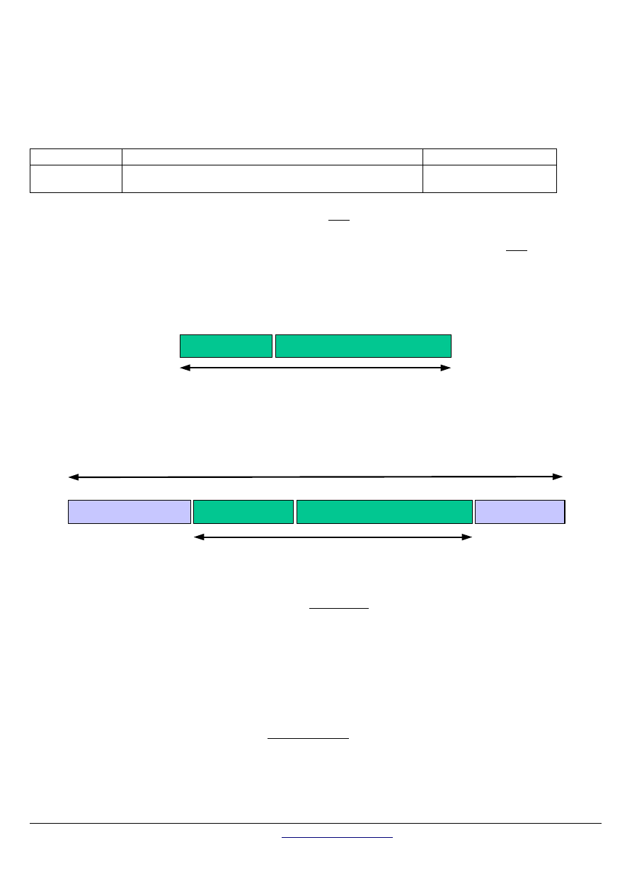
A MODBUS message is placed by the transmitting device into a frame that has a known beginning and ending point. This allows
devices that receive a new frame to begin at the start of the message, and to know when the message is completed. Partial
messages must be detected and errors must be set as a result.
In RTU mode, message frames are separated by a silent interval of at least 3.5 character times. In the following sections, this time
interval is called t3,5.
t
0
at least 3.5 char
Frame 1
Frame 2
at least 3.5 char
Frame 3
4.5 char
3.5 char
Start
Address Function
Data
CRC Check
≥
3.5 char
8 bits
8 bits
N x 8 bits
16 bits
End
≥
3.5 char
MODBUS message
Figure 13:
RTU Message Frame
The entire message frame must be transmitted as a continuous stream of characters.
If a silent interval of more than 1.5 character times occurs between two characters, the message frame is declared incomplete and
should be discarded by the receiver.
t
0
≤
1.5 char
Frame 1 OK
Frame 2 NOK
> 1.5 char
Remark :
The implementation of RTU reception driver may imply the management of a lot of interruptions due to the t
1.5
and t
3.5
timers. With
high communication baud rates, this leads to a heavy CPU load. Consequently these two timers must be strictly respected when the
baud rate is equal or lower than 19200 Bps. For baud rates greater than 19200 Bps, fixed values for the 2 timers should be used: it is
recommended to use a value of 750µs for the inter-character time-out (t
1.5
) and a value of 1.750ms for inter-frame delay (t
3.5
).
MODBUS over serial line specification and implementation guide V1.02
Modbus-IDA.ORG
Modbus.org
http://www.modbus.org/ 14/44
Dec 20, 2006
The following drawing provides a description of the RTU transmission mode state diagram. Both "master" and "slave" points of view
are expressed in the same drawing :
Character received
/ flag = frame NOK
Emission
Reception
First character received
/ init. and start t
1.5,
t
3.5
Emitted character
[if last emitted character]
/ init. and start t
3.5
Demand of emission
Character received
/ init. and start t
1.5,
t
3.5
t
1.5
expired
Legend
t
1.5,
t
3.5
: timers
t
3.5
: 3.5 character times
t
1.5
: 1.5 character times
Control and
Waiting
Initial State
t
3.5
expired
Idle
/start t
3.5
Comment
If frame OK
processing frame
If frame NOK
delete entire frame
Comment
control frame (CRC, Parity, Slave addr)
flag = frame OK or NOK
t
3.5
expired
t
3.5
expired
Character received
/ init. and start t
3.5
(ready to receive or to emit)
Figure 14:
RTU transmission mode state diagram
Some explanations about the above state diagram:
Transition from "Initial State" to "Idle" state needs t
3.5
time-out expiration : that insures inter-frame delay
"Idle" state is the normal state when neither emission nor reception is active.
In RTU mode, the communication link is declared in "idle" state when there is no transmission activity after a time interval equal to
at least 3,5 characters.
When the link is in idle state, each transmitted character detected on the link is identified as the start of a frame. The link goes to
the "active" state. Then, the end of frame is identified when no more character is transmitted on the link after the time interval
t3,5.
After detection of the end of frame, the CRC calculation and checking is completed. Afterwards the address field is analysed to
determine if the frame is for the device. If not the frame is discarded. In order to reduce the reception processing time the
address field can be analysed as soon as it is received without waiting the end of frame. In this case the CRC will be calculated
and checked only if the frame is addressed to the slave (broadcast frame included).
2.5.1.2 CRC
Checking
The RTU mode includes an error–checking field that is based on a Cyclical Redundancy Checking (CRC) method performed on the
message contents.
The CRC field checks the contents of the entire message. It is applied regardless of any parity checking method used for the
individual characters of the message.
The CRC field contains a 16–bit value implemented as two 8–bit bytes.
The CRC field is appended to the message as the last field in the message. When this is done, the low–order byte of the field is
appended first, followed by the high–order byte. The CRC high–order byte is the last byte to be sent in the message.
The CRC value is calculated by the sending device, which appends the CRC to the message. The receiving device recalculates a
CRC during receipt of the message, and compares the calculated value to the actual value it received in the CRC field. If the two
values are not equal, an error results.
The CRC calculation is started by first pre-loading a 16–bit register to all 1’s. Then a process begins of applying successive 8–bit
bytes of the message to the current contents of the register. Only the eight bits of data in each character are used for generating the
CRC. Start and stop bits and the parity bit, do not apply to the CRC.

MODBUS over serial line specification and implementation guide V1.02
Modbus-IDA.ORG
Modbus.org
http://www.modbus.org/
15/44
Dec 20, 2006
During generation of the CRC, each 8–bit character is exclusive ORed with the register contents. Then the result is shifted in the
direction of the least significant bit (LSB), with a zero filled into the most significant bit (MSB) position. The LSB is extracted and
examined. If the LSB was a 1, the register is then exclusive ORed with a preset, fixed value. If the LSB was a 0, no exclusive OR takes
place.
This process is repeated until eight shifts have been performed. After the last (eight) shift, the next 8–bit byte is exclusive ORed with
the register’s current value, and the process repeats for eight more shifts as described above. The final content of the register, after all
the bytes of the message have been applied, is the CRC value.
When the CRC is appended to the message, the low-order byte is appended first, followed by the high-order byte. A detailed example
of CRC generation is contained in Appendix B.

MODBUS over serial line specification and implementation guide V1.02
Modbus-IDA.ORG
Modbus.org
http://www.modbus.org/ 16/44
Dec 20, 2006
2.5.2
The ASCII Transmission Mode
When devices are setup to communicate on a MODBUS serial line using ASCII (American Standard Code for Information
Interchange) mode, each 8–bit byte in a message is sent as two ASCII characters. This mode is used when the physical
communication link or the capabilities of the device does not allow the conformance with RTU mode requirements regarding timers
management.
Remark : this mode is less efficient than RTU since each byte needs two characters.
Example : The byte 0X5B is encoded as two characters : 0x35 and 0x42 ( 0x35 ="5", and 0x42 ="B" in ASCII ).
The format ( 10 bits ) for each byte in ASCII mode is :
Coding System:
Hexadecimal, ASCII characters 0–9, A–F
One hexadecimal character contains 4-bits of data within each ASCII character of the message
Bits per Byte:
1 start bit
7 data bits, least significant bit sent first
1 bit for parity completion;
1 stop bit
Even parity is required, other modes ( odd parity, no parity ) may also be used. In order to ensure a maximum compatibility with
other products, it is recommended to support also No parity mode. The default parity mode must be Even parity.
Remark : the use of no parity requires 2 stop bits.
How Characters are Transmitted Serially :
Each character or byte is sent in this order (left to right):
Least Significant Bit (LSB) . . . Most Significant Bit (MSB)
Start
With Parity Checking
1
2
3
4
5
6
7
Par Stop
Figure 15:
Bit Sequence in ASCII mode
Devices may accept by configuration either Even, Odd, or No Parity checking. If No Parity is implemented, an additional stop bit is
transmitted to fill out the character frame :
Start
Without Parity Checking
1
2
3
4
5
6
7
Stop Stop
Figure 16:
Bit Sequence in ASCII mode (specific case of No Parity)
Frame Checking Field: Longitudinal Redundancy Checking (LRC)
MODBUS over serial line specification and implementation guide V1.02
Modbus-IDA.ORG
Modbus.org
http://www.modbus.org/
17/44
Dec 20, 2006
2.5.2.1
MODBUS Message ASCII Framing
A MODBUS message is placed by the transmitting device into a frame that has a known beginning and ending point. This allows
devices that receive a new frame to begin at the start of the message, and to know when the message is completed. Partial
messages must be detected and errors must be set as a result.
The address field of a message frame contains two characters.
In ASCII mode, a message is delimited by specific characters as Start-of-frames and End-of-frames. A message must start with a
‘colon’ ( : ) character (ASCII 3A hex), and end with a ‘carriage return – line feed’ (CRLF) pair (ASCII 0D and 0A hex).
Remark : The LF character can be changed using a specific MODBUS application command ( see MODBUS application protocol
specification).
The allowable characters transmitted for all other fields are hexadecimal 0–9, A–F (ASCII coded). The devices monitor the bus
continuously for the ‘colon’ character. When this character is received, each device decodes the next character until it detects the
End-Of-Frame.
Intervals of up to one second may elapse between characters within the message. Unless the user has configured a longer timeout,
an interval greater than 1 second means an error has occurred. Some Wide-Area-Network application may require a timeout in the 4
to 5 second range.
A typical message frame is shown below.
Start
Address
Function
Data
LRC
End
1 char
:
2 chars
2 chars
2 chars
2 chars
CR,LF
0 up to 2x252 char(s)
Figure 17:
ASCII Message Frame
Remark : Each data byte needs two characters for encoding. Thus, to ensure compatibility at MODBUS application level between
ASCII mode and RTU mode, the maximum data size for ASCII data field (2x252) is the double the maximum data size for RTU data
field (252). Consequently, the maximum size of a MODBUS ASCII frame is 513 characters.
The ASCII framing requirements are synthesized in the following state diagram. Both "master" and "slave" points of view are
expressed in the same drawing :
Reception
Reception of ":"
character
Reception of character
/ Concatenation of
character into
reception buffer
Waiting "End
of Frame"
Idle
Comment
If frame OK
processing frame
If frame NOK
delete entire frame
(ready to receive or to emit)
Reception of "LF" character
/ control frame (LRC, Parity,
Slave addr.)
Reception of ":"
character / Empty
reception buffer
Reception of "CR"
character
Reception of ":"
character / Empty
reception buffer
Emission
start
Emission Demand
Emission
Sending of “:”
Sending of
all characters
Emission End
Sending of “CR”
Sending of “LF”
Figure 18:
ASCII Transmission mode State diagram

MODBUS over serial line specification and implementation guide V1.02
Modbus-IDA.ORG
Modbus.org
http://www.modbus.org/ 18/44
Dec 20, 2006
Some explanations about the above state diagram :
"Idle" state is the normal state when neither emission nor reception is active.
Each reception of a ":" character means a beginning of a new message. If a message was in process of reception while receiving
such a character, the current message is declared incomplete and it is discarded. A new reception buffer is then allocated.
After detection of the end of frame, the LRC calculation and checking is completed. Afterwards the address field is analyzed to
determine if the frame is for the device. If not the frame is discarded. In order to reduce the reception processing time the
address field can be analyzed as soon as it is reserved without waiting the end of frame.
2.5.2.2 LRC
Checking
In ASCII mode, messages include an error–checking field that is based on a Longitudinal Redundancy Checking (LRC) calculation
that is performed on the message contents, exclusive of the beginning ‘colon’ and terminating CRLF pair characters. It is applied
regardless of any parity checking method used for the individual characters of the message.
The LRC field is one byte, containing an 8–bit binary value. The LRC value is calculated by the device that emits, which appends the
LRC to the message. The device that receives calculates an LRC during receipt of the message, and compares the calculated value
to the actual value it received in the LRC field. If the two values are not equal, an error results.
The LRC is calculated by adding together successive 8–bit bytes of the message, discarding any carries, and then two’s
complementing the result. It is performed on the bytes of the message, before the encoding of each byte in the two ASCII
characters corresponding to the hexadecimal representation of each nibble. The computation does not include the 'colon' character
that begins the message, and does not include the CRLF pair at the end of the message.
The resulting LRC is ASCII encoded into two bytes and placed at the end of the ASCII mode frame before the CRLF.
A detailed example of LRC generation is contained in Appendix B.

MODBUS over serial line specification and implementation guide V1.02
Modbus-IDA.ORG
Modbus.org
http://www.modbus.org/
19/44
Dec 20, 2006
2.6
Error Checking Methods
The security of standard MODBUS Serial Line is based on two kinds of error checking :
Parity checking (even or odd) should be applied to each character.
Frame checking (LRC or CRC) must be applied to the entire message.
Both the character checking and message frame checking are generated in the device (master or slave) that emits and applied to the
message contents before transmission. The device (slave or master) checks each character and the entire message frame during
receipt.
The master is configured by the user to wait for a predetermined timeout interval ( Response time-out) before aborting the transaction.
This interval is set to be long enough for any slave to respond normally ( unicast request). If the slave detects a transmission error, the
message will not be acted upon. The slave will not construct a response to the master. Thus the timeout will expire and allow the
master’s program to handle the error. Note that a message addressed to a nonexistent slave device will also cause a timeout.
2.6.1 Parity
Checking
Users may configure devices for Even ( required) or Odd Parity checking, or for No Parity checking ( recommended). This will
determine how the parity bit will be set in each character.
If either Even or Odd Parity is specified, the quantity of 1 bits will be counted in the data portion of each character (seven data bits for
ASCII mode, or eight for RTU). The parity bit will then be set to a 0 or 1 to result in an Even or Odd total of 1 bits.
For example, these eight data bits are contained in an RTU character frame:
1100 0101
The total quantity of 1 bits in the frame is four. If Even Parity is used, the frame’s parity bit will be a 0, making the total quantity of 1 bits
still an even number (four). If Odd Parity is used, the parity bit will be a 1, making an odd quantity (five).
When the message is transmitted, the parity bit is calculated and applied to the frame of each character. The device that receives
counts the quantity of 1 bits and sets an error if they are not the same as configured for that device (all devices on the MODBUS Serial
Line must be configured to use the same parity checking method).
Note that parity checking can only detect an error if an odd number of bits are picked up or dropped in a character frame during
transmission. For example, if Odd Parity checking is employed, and two 1 bits are dropped from a character containing three 1 bits,
the result is still an odd count of 1 bits.
If No Parity checking is specified, no parity bit is transmitted and no parity checking can be made. An additional stop bit is transmitted
to fill out the character frame.
2.6.2 Frame
Checking
Two kinds of frame checking is used depending on the transmission mode, RTU or ASCII.
In RTU mode, messages include an error–checking field that is based on a Cyclical Redundancy Checking (CRC) method. The
CRC field checks the contents of the entire message. It is applied regardless of any parity checking method used for the individual
characters of the message.
In ASCII mode, messages include an error–checking field that is based on a Longitudinal Redundancy Checking (LRC) method.
The LRC field checks the contents of the message, exclusive of the beginning ‘colon’ and ending CRLF pair. It is applied
regardless of any parity checking method used for the individual characters of the message.
The detailed information about error checking methods is contained in the previous sections.

MODBUS over serial line specification and implementation guide V1.02
Modbus-IDA.ORG
Modbus.org
http://www.modbus.org/ 20/44
Dec 20, 2006
3 Physical
Layer
3.1 Preamble
A new MODBUS solution over serial line should implement an electrical interface in accordance with EIA/TIA-485 standard ( also
known as RS485 standard). This standard allows point to point and multipoint systems, in a “two-wire configuration”. In addition, some
devices may implement a “Four-Wire” RS485-Interface.
A device may also implement an RS232-Interface.
In such a MODBUS system, a Master Device and one or several Slave Devices communicate on a passive serial line.
On standard MODBUS system, all the devices are connected (in parallel) on a trunk cable constituted by 3 conductors. Two of those
conductors ( the “Two-Wire” configuration ) form a balanced twisted pair, on which bi-directional data are transmitted, typically at the
bit rate of 9600 bits per second.
Each device may be connected ( see figure 19):
-
either directly on the trunk cable, forming a daisy-chain,
-
either on a passive Tap with a derivation cable,
-
either on an active Tap with a specific cable.
Screw Terminals, RJ45, or D-shell 9 connectors may be used on devices to connect cables (see the chapter “Mechanical Interfaces”).
3.2
Data Signaling Rates
9600 bps and 19.2 Kbps are required and 19.2 is the required default
Other baud rates may optionally be implemented : 1200, 2400, 4800, … 38400 bps, 56 Kbps, 115 Kbps, …
Every implemented baud rate must be respected better than 1% in transmission situation, and must accept an error of 2% in reception
situation.
MODBUS over serial line specification and implementation guide V1.02
Modbus-IDA.ORG
Modbus.org
http://www.modbus.org/
21/44
Dec 20, 2006
3.3 Electrical
Interfaces
3.3.1
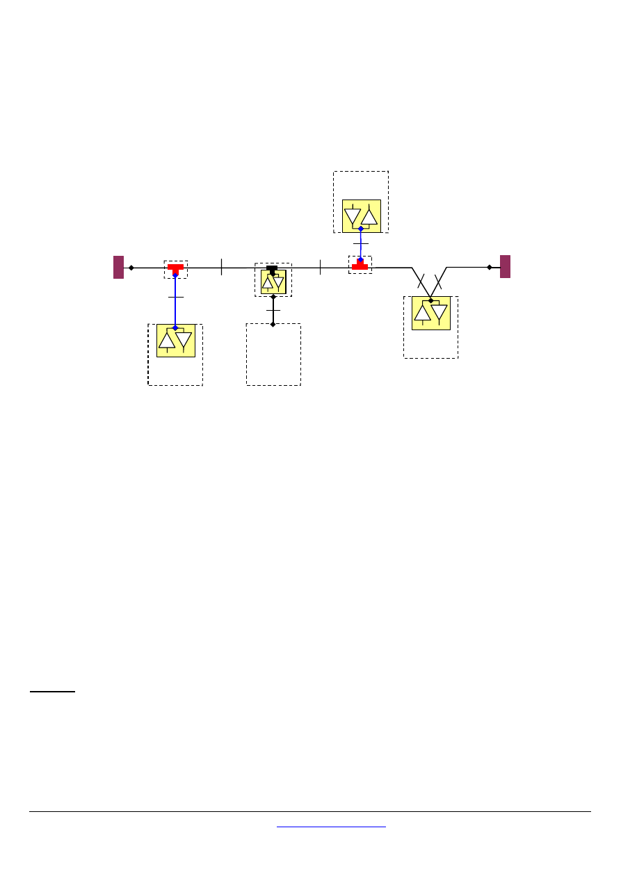
Multipoint Serial Bus Infrastructure
Figure 19 gives a general overview of the serial bus infrastructure in a MODBUS multipoint Serial Line system.
Slave n
D
R
ITr
LT
ITr
ITr
LT
Passive TAP
IDv
Slave 1
D
R
Master
IDv
D
R
ActiveTap
AUI
Slave 2
D
R
Passive TAP
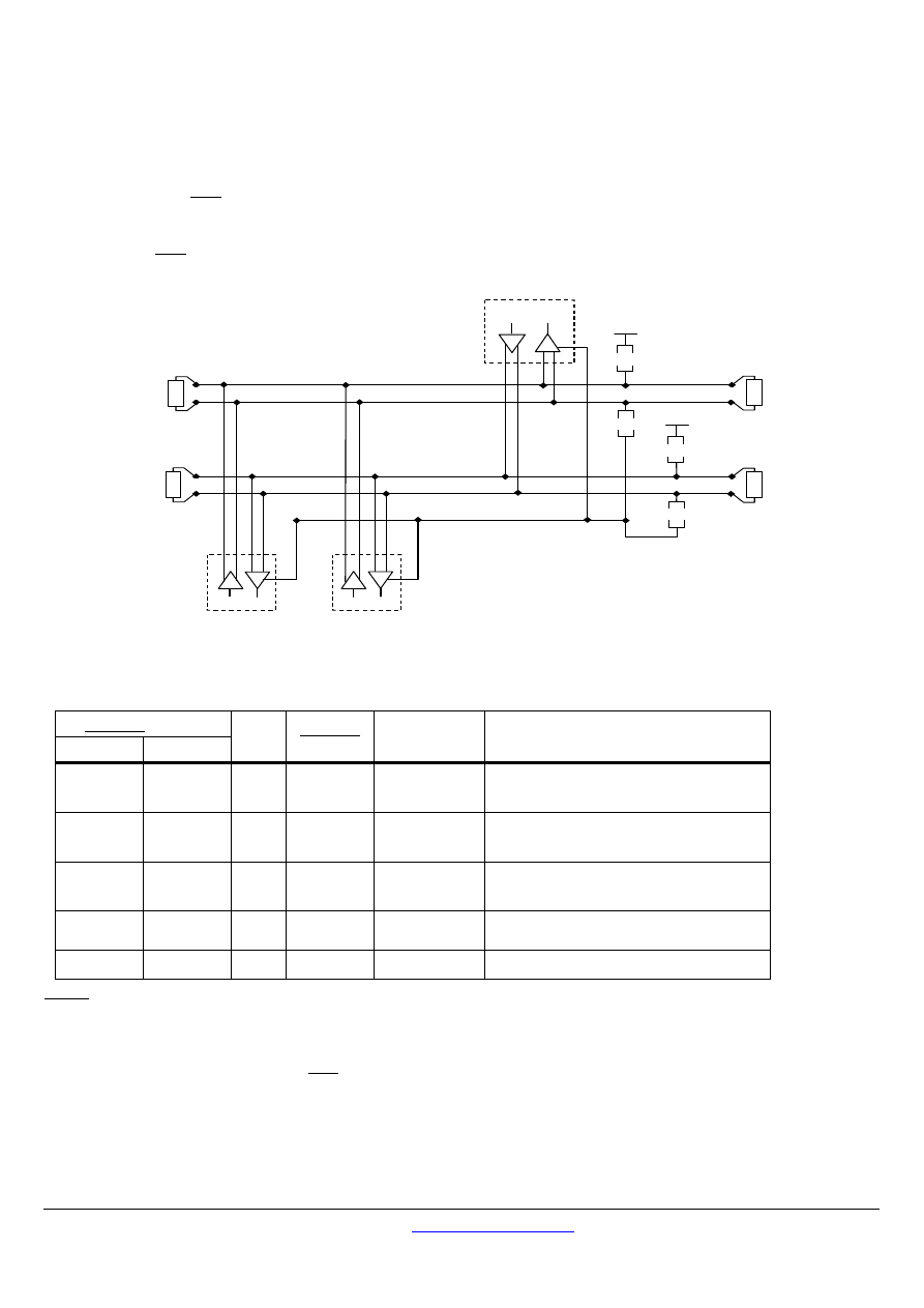
Figure 19 : Serial bus infrastructure
A multipoint MODBUS Serial Line bus is made of a principal cable (
the Trunk
), and possibly some
derivation
cables.
Line terminations are necessary at each extremity of the trunk cable for impedance adaptation (see § "Two-Wire MODBUS Definition"
& "Optional Four-Wire MODBUS Definition" for details).
As shown in figure 19, different implementations may operate in the same MODBUS Serial Line system :
the device integrates the communication transceiver and is connected to the trunk using a
Passive Tap
and a derivation cable
( case of Slave 1 and Master )
;
the device doesn't integrate the communication transceiver and is connected to the trunk using an
Active Tap
and a derivation
cable (the active TAP integrates the transceiver)
( case of Slave 2 )
;
the device is connected directly to the trunk cable, in a
Daisy-Chain ( case of Slave n )
The following conventions are adopted :
The interface with the trunk is named
ITr
(Trunk Interface)
The interface between the device and the Passive Tap is named
IDv
(Derivation Interface)
The interface between the device and the Active Tap is named
AUI
(Attachment Unit Interface)
Remarks :
1. In some cases, the Tap may be connected directly to the IDv-socket or the AUI-socket of the device, without using a derivation
cable.
2. A Tap may have several IDv sockets to connect several devices. Such a Tap is named Distributor when it is a passive one.
3. When using an active Tap, power supply of the Tap may be provided either via its AUI or ITr interface.
ITr and IDv interfaces are described in the following chapters (see § "Two-Wire MODBUS DEFINITION" & "Four-Wire MODBUS
DEFINITION").
MODBUS over serial line specification and implementation guide V1.02
Modbus-IDA.ORG
Modbus.org
http://www.modbus.org/ 22/44
Dec 20, 2006
3.3.2
Two-Wire MODBUS Definition
A MODBUS solution over serial line should implement a “Two-Wire” electrical interface in accordance with EIA/TIA-485 standard.
On such a 2W-bus, at any time one driver only has the right for transmitting.
In fact a third conductor must also interconnect all the devices of the bus : the common.
Pull Up
5 V
Pull Down
Common
D
R
Master
D
R
Slave 1
Slave n
D1
D0
D
R
LT
LT
Balanced Pair
Figure 20:
General 2-Wire Topology
2W-MODBUS Circuits Definition
Required Circuits
on ITr
on IDv
For
device
Required
on device
EIA/TIA-485
name
Description
D1
D1 I/O X
B/B’
Transceiver terminal 1, V1 Voltage
( V1 > V0 for binary 1 [OFF] state )
D0
D0 I/O X
A/A’
Transceiver terminal 0, V0 Voltage
( V0 > V1 for binary 0 [ON] state )
Common
Common --
X
C/C’
Signal and optional Power Supply Common
Notes :
•
For Line Termination (LT), Pull Up and Pull Down resistors, please refer to section “Multipoint System requirements".
•
D0, D1, and Common circuit names must be used in the documentation related to the device and the Tap ( User Guide, Cabling
Guide, … ) to facilitate interoperability.
•
Optional electrical interfaces may be added, for example :
Power Supply :
5..24 V D.C.
Port mode control : PMC circuit ( TTL compatible ). When needed, port mode may be controlled either by this external
circuit and/or by another way (a switch on the device for example). In the first case while an open circuit PMC will ask for the
2W-MODBUS mode, a Low level on PMC will switch the port into 4W-MODBUS or RS232-MODBUS Mode, depending on the
implementation.
MODBUS over serial line specification and implementation guide V1.02
Modbus-IDA.ORG
Modbus.org
http://www.modbus.org/
23/44
Dec 20, 2006
3.3.3
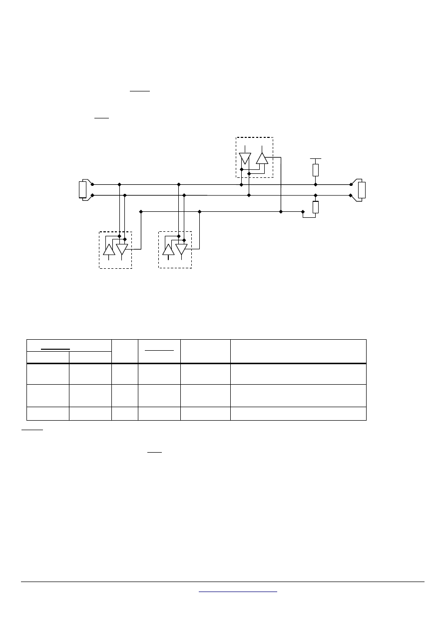
Optional Four-Wire MODBUS Definition
Optionally, such MODBUS devices also permit to implement a 2-pair bus (4 wires) of mono directional data. The data on the master
pair ( RXD1-RXD0 ) are only received by the slaves ; the data on the slave pair ( TXD1-TXD0 ) are only received by the only master.
In fact a fifth conductor must also interconnect all the devices of the 4W-bus : the common.
In the same way as on a 2W-MODBUS, at any time one driver only has the right for emitting.
Such a device must implement, for each balanced pair, a driver and a transceiver in accordance with EIA/ TIA-485.
( Sometimes this solution has been named “RS422”, which is not correct : the RS422 standard does not support several drivers on
one balanced pair.)
C o m m o n
D
R
S la v e 1
S la v e n
T X D 0
D
R
T X D 1
5 V
L T
D
R
M a s te r
R X D 1
R X D 0
L T
5 V
L T
L T
P u ll D o w n
P u ll U p
P u ll D o w n
P u ll U p
M a s te r P a ir
S la v e P a ir
Figure 21:
General 4-wire topology
Optional 4W-MODBUS Circuits Definition
Required Circuits
on ITr
on IDv
For
device
Required
on device
EIA/TIA-485
name
Description for IDv
TXD1
TXD1 Out
X
B
Generator terminal 1, Vb Voltage
( Vb > Va for binary 1 [OFF] state )
TXD0
TXD0 Out
X
A
Generator terminal 0, Va Voltage
( Va > Vb for binary 0 [ON] state )
RXD1
RXD1 In (1)
B’
Receiver terminal 1, Vb’ Voltage
( Vb’ > Va’ for binary 1 [OFF] state )
RXD0
RXD0 In (1)
A’
Receiver terminal 0, Va’ Voltage
( Va’ > Vb’ for binary 0 [ON] state )
Common
Common --
X
C/C’
Signal and optional Power Supply Common
Notes :
•
For Line Termination (LT), Pull Up and Pull Down resistors, please refer to section “Multipoint System requirements".
•
Those circuits (1) are required only if an 4W-MODBUS option is implemented.
•
The name of the 5 required circuits must be used in the documentation related to the device and the Tap ( User Guide, Cabling
Guide, … ) to facilitate interoperability.
•
Optional electrical interfaces may be added, for example :
Power Supply : 5..24 V D.C.
PMC circuit : See above ( In 2W-MODBUS Circuits Definition ) the note about this optional circuit.

MODBUS over serial line specification and implementation guide V1.02
Modbus-IDA.ORG
Modbus.org
http://www.modbus.org/ 24/44
Dec 20, 2006
3.3.3.1
4W-Cabling System Important Topic
In such a 4W-MODBUS, Master Device and Slave Devices have IDv interfaces with the same 5 required circuits.
As the master has to :
-
receive from the slave the data on the slave pair ( TXD1-TXD0 ),
-
and transmit on the master pair ( RXD1-RXD0 , received by the slaves) ,
the 4W-cabling system must cross the two pairs of the bus between ITr and the IDv of the master :
Signal on Master IDv
Name Type
EIA/TIA-485
Name
Circuit on ITr
RXD1
In
B’
TXD1
Slave Pair
RXD0
In
A’
TXD0
TXD1
Out
B
RXD1
Master Pair
TXD0
Out
A
RXD0
Common --
C/C’ Common
This crossing may be implemented by crossed cables, but the connection of such crossed cables in a 2-wire system may cause
damages. To connect a 4W master device ( which have a MODBUS connector) a better solution is to use a Tap which includes the
crossing function.
3.3.3.2
Compatibility between 4-Wire and 2-Wire cabling
In order to connect devices implementing a 2-Wire physical interface to an already existing 4-Wire system, the 4-Wire cabling system
can be modified as described below :
TxD0 signal shall be wired with the RxD0 signal, turning them to the D0 signal
TxD1 signal shall be wired with the RxD1 signal, turning them to the D1 signal.
Pull-up, Pull-down and line terminations resistors shall be re-arranged to correctly adapt the D0, D1 signals.
MODBUS over serial line specification and implementation guide V1.02
Modbus-IDA.ORG
Modbus.org
http://www.modbus.org/
25/44
Dec 20, 2006
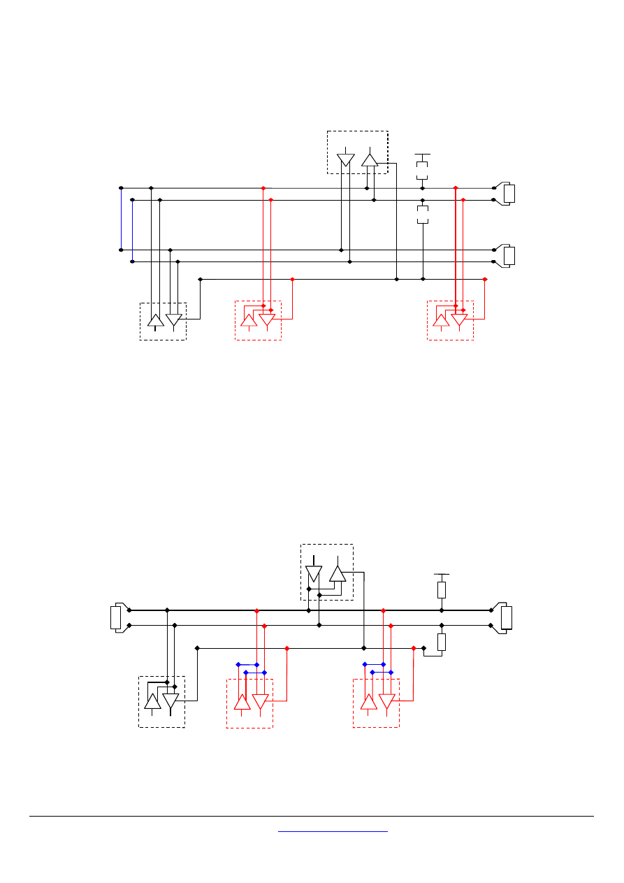
The figure hereafter gives an example where slaves 2 and 3 which use a 2-Wire interface can operate with the Master and the slave 1
which use a 4-Wire interface.
C o m m o n
D
R
S la v e 1
T X D 0
T X D 1
D
R
M a s te r
R X D 1
R X D 0
5 V
L T
L T
P u ll D o w n
P u ll U p
S la v e 2
D
R
S la v e 3
D
R
Figure 22 : Changing a 4-Wire cabling system into a 2-Wire cabling system
In order to connect devices implementing a 4-Wire physical interface to an already existing 2-Wire system, the 4-Wire interface of the
new coming devices can be arranged as describe below :
On each 4-Wire device interface :
TxD0 signal shall be wired with the RxD0 signal and then connected to the D0 signal of the trunk ;
TxD1 signal shall be wired with the RxD1 signal and then connected to the D1 signal of the trunk.
The figure hereafter gives an example where slaves 2 and 3 which use a 4-Wire interface can operate with the Master and the slave 1
which use a 2-Wire interface.
Pull Up
5 V
Pull Down
Common
D
R
Slave 1
D1
D0
LT
LT
D
R
Master
Balanced Pair
D
R
Slave 2
D
R
Slave 3
Figure 23 : Connecting devices with 4-Wire interface to a 2-Wire cabling system

MODBUS over serial line specification and implementation guide V1.02
Modbus-IDA.ORG
Modbus.org
http://www.modbus.org/ 26/44
Dec 20, 2006
3.3.4
RS232-MODBUS Definition
Some devices may implement an RS232-Interface between a DCE and a DTE.
Optional RS232-MODBUS Circuits Definition
Signal
For DCE
Required
on DCE (1)
Required
on DTE (1)
Description
Common --
X X
Signal Common
CTS In
Clear to Send
DCD --
Data Carrier Detected ( from DCE to DTE )
DSR In
Data Set Ready
DTR Out
Data Terminal Ready
RTS Out
Request to Send
RXD In
X X
Received Data
TXD Out
X X
Transmitted Data
Notes :
•
“X” marked signals are required only if an RS232-MODBUS option is implemented.
•
Signals are in accordance with EIA/ TIA-232.
•
Each TXD must be wired with RXD of the other device ;
•
RTS may be wired with CTS of the other device,
•
DTR may be wired with DSR of the other device.
•
Optional electrical interfaces may be added, for example :
Power Supply :
5..24 V D.C.
PMC circuit :
See above ( In 2W-MODBUS Circuits Definition ) the note about this optional circuit.
3.3.5 RS232-MODBUS
requirements
This optional MODBUS on Serial Line system should only be used for short length ( typically less than 20m ) point to point inter-
connection.
Then, the EIA/TIA-232 standard must be respected :
⇒ circuits definition,
⇒ maximum wire capacitance to ground ( 2500 pF, then 25 m for a 100 pF/m cable ).
Please refer to chapter “Cables” for the shield, and for the possibility to use Category 5 Cables.
Documentation of the device must indicate :
⇒ if the device must be considered as a DCE either as a DTE,
⇒ how optional circuits must work if such is the case.

MODBUS over serial line specification and implementation guide V1.02
Modbus-IDA.ORG
Modbus.org
http://www.modbus.org/
27/44
Dec 20, 2006
3.4
Multipoint System requirements
For any EIA/ TIA-485 multipoint system, in either 2-wire or 4-wire configuration, the following requirements all apply.
3.4.1
Maximum number of devices without repeater
A figure of 32 devices is always authorized on any RS485-MODBUS system without repeater.
Depending of :
- all the possible addresses,
- the figure of RS485 Unit Load used by the devices,
- and the line polarization in need be,
A RS485 system may implement a larger number of devices. Some devices allow the implementation of a RS485-MODBUS serial line
with more than 32 devices, without repeater.
In this case these MODBUS devices must be documented to say how many of such devices are authorized without repeater.
The use of a repeater between two heavy loaded RS485-MODBUS is also possible.
3.4.2 Topology
An RS485-MODBUS configuration without repeater has one trunk cable, along which devices are connected, directly (daisy chaining)
or by short derivation cables.
The trunk cable, also named “Bus”, can be long (see hereafter). Its two ends must be connected on Line Terminations.
The use of repeaters between several RS485-MODBUS is also possible.
3.4.3 Length
The end to end length of the trunk cable must be limited. The maximum length depends on the baud rate, the cable (Gauge,
Capacitance or Characteristic Impedance), the number of loads on the daisy chain, and the network configuration (2-wire or 4-wire).
For a maximum 9600 Baud Rate and AWG26 (or wider) gauge, the maximum length is 1000m. In the specific case shown in the figure
22 ( 4 Wire cabling used as a 2 Wire cabling system) the maximum length must be divided by two.
The derivations must be short, never more than 20m. If a multi-port tap is used with n derivations, each one must respect a maximum
length of 40m divided by n.
3.4.4 Grounding
Arrangements
The « Common » circuit ( Signal and optional Power Supply Common ) must be connected directly to protective ground, preferably at
one point only for the entire bus. Generally this point is to choose on the master device or on its Tap.
3.4.5 Line
Termination
A reflection in a transmission line is the result of an impedance discontinuity that a travelling wave sees as it propagates down the line.
To minimize the reflections from the end of the RS485-cable it is required to place a Line Termination near each of the 2 Ends of the
Bus.
It is important that the line be terminated at both ends since the propagation is bi-directional, but it is not allowed to place more than 2
LT on one passive D0-D1 balanced pair . Never place any LT on a derivation cable.

MODBUS over serial line specification and implementation guide V1.02
Modbus-IDA.ORG
Modbus.org
http://www.modbus.org/ 28/44
Dec 20, 2006
Each line termination must be connected between the two conductors of the balanced line : D0 and D1.
Line termination may be a 150 ohms value ( 0.5 W ) resistor.
A serial capacitor ( 1 nF, 10 V minimum ) with a 120 Ohms ( 0.25 W ) resistor is a better choice when a polarization of the pair must
be implemented (see here after).
In a 4W-system, each pair must be terminated at each end of the bus.
In an RS232 interconnections, no termination should be wired.
3.4.6 Line
Polarization
When there is no data activity on an RS-485 balanced pair, the lines are not driven and, thus susceptible to external noise or
interference. To insure that its receiver stays in a constant state, when no data signal is present, some devices need to bias the
network.
Each MODBUS device must be documented to say :
-
if the device needs a line polarization,
-
if the device implements, or can implement, such a line polarization.
If one or several devices need polarization, one pair of resistors must be connected on the RS-485 balanced pair :
-
a Pull-Up Resistor to a 5V Voltage on D1 circuit,
-
a Pull-Down Resistor to the common circuit on D0 circuit.
The value of those resistors must be between 450 Ohms and 650 Ohms. 650 Ohms resistors value may allow a higher number of
devices on the serial line bus.
In this case, a polarization of the pair must be implemented at one location for the whole Serial Bus. Generally this point is to
choose on the master device or on its Tap. Other devices must not implement any polarization.
The maximum number of devices authorized on such a MODBUS Serial Line is reduced by 4 from a MODBUS without polarization.
MODBUS over serial line specification and implementation guide V1.02
Modbus-IDA.ORG
Modbus.org
http://www.modbus.org/
29/44
Dec 20, 2006
3.5 Mechanical
Interfaces
Screw Terminals may be used for both IDv and ITr connections. All information must be provided to the users about the exact
location of each signal, with names in accordance with the previous chapter “Electrical Interface”.
If a RJ45 ( or a mini-DIN or a D-Shell) connector is used on an equipment for a MODBUS mechanical interface, a shielded female
connector must be chosen. Then the cable-end must have a shielded male connector.
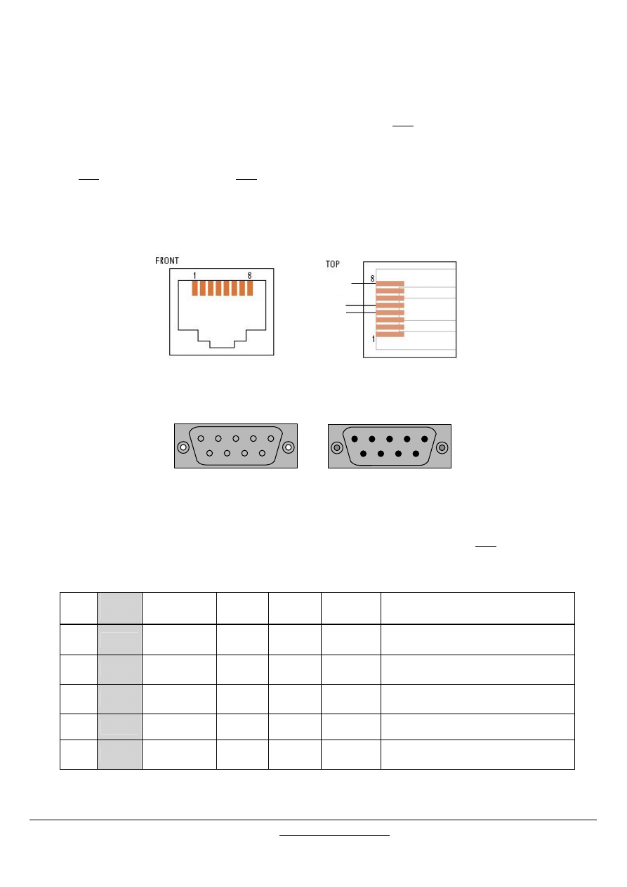
3.5.1
Connectors pin-out for 2W-MODBUS
Device side - female connector
D0
D1
Common
Figure 24:
2W- MODBUS on RJ45 connector ( required pin-out )
Male (Front view)
1
2
3
4
5
6
7
8
9
Female (Front view)
5
4
3
2
1
9
8
7
6
Figure 25:
D-shell 9-pin connector
Screw type connectors can also be used.
If an RJ45 or a 9-pin D-shell connector is used for a standard MODBUS device, the pinouts hereafter must be respected for every
implemented circuit.
2W-MODBUS RJ45 and 9-pin D-shell Pinouts
Pin on
RJ45
Pin on
D9-shell
Level of
requirement
IDv
Circuit
ITr
Circuit
EIA/TIA-
485 name
Description for IDv
3
3
optional
PMC
--
--
Port Mode Control
4
5
required
D1 D1 B/B’
Transceiver terminal 1, V1 Voltage
( V1 > V0 for binary 1 [OFF] state )
5
9
required
D0
D0 A/A’
Transceiver terminal 0, V0 Voltage
( V0 > V1 for binary 0 [ON] state )
7
2
recommended
VP
--
--
Positive 5...24 V D.C. Power Supply
8
1
required
Common Common
C/C’
Signal and Power Supply Common
MODBUS over serial line specification and implementation guide V1.02
Modbus-IDA.ORG
Modbus.org
http://www.modbus.org/ 30/44
Dec 20, 2006
3.5.2
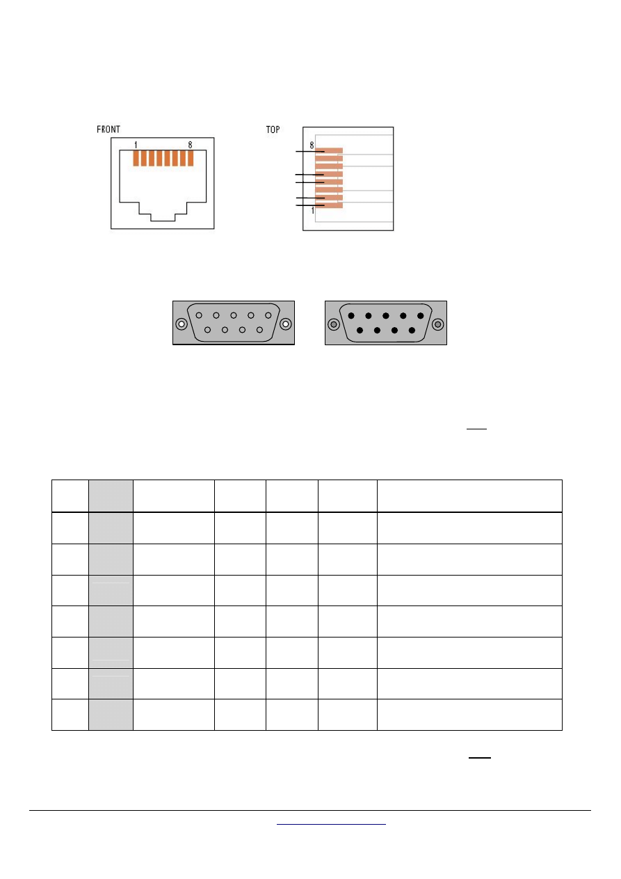
Connectors pin-out for optional 4W-MODBUS
Device side - female connector
Figure 26:
4W- MODBUS on RJ45 connector ( required pin-out )
Male (Front view)
1
2
3
4
5
6
7
8
9
Female (Front view)
5
4
3
2
1
9
8
7
6
Figure 27:
D-shell 9-pin connector
Screw type connectors can also be used.
If an RJ45 or a 9-pin D-shell connector is used for a 4W-MODBUS device, the pinouts hereafter must be respected for every
implemented circuit.
Optional 4W-MODBUS RJ45 and 9-pin D-shell Pinouts
Pin on
RJ45
Pin on
D9-shell
Level of
requirement
IDv
Signal
ITr
Signal
EIA/TIA-
485 name
Description for IDv
1
8
required
RXD0
RXD0
A’
Receiver terminal 0, Va’ Voltage
( Va’ > Vb’ for binary 0 [ON] state )
2
4
required
RXD1
RXD1
B’
Receiver terminal 1, Vb’ Voltage
( Vb’ > Va’ for binary 1 [OFF] state )
3
3
optional
PMC
--
--
Port Mode Control
4
5
required
TXD1
TXD1
B
Generator terminal 1, Vb Voltage
( Vb > Va for binary 1 [OFF] state )
5
9
required
TXD0
TXD0
A
Generator terminal 0, Va Voltage
( Va > Vb for binary 0 [ON] state )
7
2
recommended
VP
--
--
Positive 5...24 V DC Power Supply
8
1
required
Common
Common
C/C’
Signal and Power Supply Common
Note : When both 2 and 4-Wire configurations are implemented on the same port, the 4W notations must be used.
Common
TXD0
TXD1
RXD1
RXD0
MODBUS over serial line specification and implementation guide V1.02
Modbus-IDA.ORG
Modbus.org
http://www.modbus.org/
31/44
Dec 20, 2006
3.5.3
RJ45 and 9-pin D-shell Pinouts for optional RS232-MODBUS
If an RJ45 or a 9-pin D-shell connector is used for a RS232-MODBUS device, the pinouts hereafter must be respected for every
implemented circuit.
DCE
Underlined pins can be output
Circuit
DTE
Underlined pins can be output
Pin on
RJ45
Pin on
D9-shell
Level of
requirement
Name Description
RS232
Source
Level of
requirement
Pin on
RJ45
Pin on D9-
shell
1
2
required
TXD
Transmitted Data
DTE
required 2
3
2
3
required
RXD
Received Data
DCE
required
1
2
3
7
optional
CTS
Clear to Send
DCE
optional
6
8
6
8
optional
RTS
Request to Send
DTE
optional
3
7
8
5
required
Common Signal Common
--
required
8
5
Important Note : Some DCE Pinouts are crossed with DTE Pinouts with the same name :
A directly pin to pin wired cable ( without any crossing ) must be used between one DTE
( a PC for example ) and a DCE (a PLC for example).

MODBUS over serial line specification and implementation guide V1.02
Modbus-IDA.ORG
Modbus.org
http://www.modbus.org/ 32/44
Dec 20, 2006
3.6 Cables
A MODBUS over Serial Line Cable must be shielded. At one end of each cable its shield must be connected to protective ground. If
a connector is used at this end, the shell of the connector is connected to the shield of the cable.
An RS485-MODBUS must use a balanced pair (for D0-D1) and a third wire (for the Common). In addition to that a second balanced
pair must be used in a 4W-MODBUS system (for RXD0-RXD1).
If a connectorized 4 pairs Category 5 Cable is used, please remember to the user in the User Guides :
“Connection of a crossed cable in a 2-wire MODBUS system may cause damages”.
To minimize errors in cabling, a Color Code is recommended for the wires in the RS485-MODBUS Cables :
Signal Names
Recommended Color
D1-TXD1 yellow
D0-TXD0 brown
Common
grey
4W ( Optional )
RXD0
white
4W ( Optional )
RXD1
blue
Figure 28:
Color code for RS485-MODBUS wires
Note :
Category 5 Cables use other colors.
For RS485-MODBUS, Wire Gauge must be chosen sufficiently wide to permit the maximum length ( 1000 m ). AWG 24 is always
sufficient for the MODBUS Data.
Category 5 cables may operate for RS485-MODBUS, to a maximum length of 600m.
For the balanced pairs used in an RS485-system, a Characteristic Impedance with a value higher than 100 Ohms may be preferred,
especially for 19200 and higher baud rates.
3.7 Visual
Diagnosis
For a visual diagnosis, communication status and device status must be indicated by LEDs :
LED
Level of requirement State
Recommended colour
Communication required
Switched ON during frame reception or sending.
( 2 LEDs for frame reception and frame sending, or 1 LED
for both purposes.)
Yellow
Error recommended
Switched ON : internal fault
Flashing : Other faults (Communication fault or
configuration error)
Red
Device status
optional
Switched ON : device powered
Green

MODBUS over serial line specification and implementation guide V1.02
Modbus-IDA.ORG
Modbus.org
http://www.modbus.org/
33/44
Dec 20, 2006
4
Installation and Documentation
4.1 Installation
Product vendor should pay attention to give to the user of a MODBUS System or MODBUS Devices all useful information to
prevent them from any error in cabling or bad utilization of cabling accessories :
-
Some other Fieldbuses, CANopen for example, use the same connector types ( D-shell, RJ45…) .
-
Studies are conducted on Ethernet, with power supply on the same Balanced Pairs Cable.
-
Some Products use for I/O circuits the same connector types ( D-shell, RJ45…).
On these connectors, for the most part, no foolproofing is available (polarizing notch or other implementation) .
4.2 User
Guide
The User Guide of any MODBUS Device or Cabling System Component must include in a non exhaustive manner one or two types of
information:
4.2.1
For any MODBUS Product :
The following information should be documented :
All the implemented requests.
The operating modes.
The visual diagnostics.
The reachable registers and supported function codes.
Installation rules.
The required information in the following sections should also be documented :
⇒ "Two-Wire MODBUS Definition" (to mention the Required Circuits) ;
⇒ "Optional Four-Wire MODBUS Definition" (to mention the Required Circuits) ;
⇒ "Line Polarization" (to mention a possible Need or an Implementation) ;
⇒ "Cables" (special care of crossed cables).
A specific indication relating to the devices addresses, is to be written in the form of an important warning :
"It is of great importance to ensure at the time of the procedure of devices addressing, that there is not two devices with the same
address. In such a case, an abnormal behavior of the whole serial bus can occur, the Master being then in the impossibility to
communicate with all present slaves on the bus."
A "Getting Started" chapter is highly recommended, with the documented description of a typical application example, for an
easy start.
4.2.2
For a MODBUS Product with implemented Options :
The different optional parameters must be clearly detailed :
⇒ Optional serial Transmission mode ;
⇒ Optional Parity Checking ;
⇒ Optional Baud Rates ;
⇒ Optional Circuit(s) : Power Supply, Port Configuration ;
⇒ Optional Interface(s) ;
⇒ Maximum number of devices (without repeater) if greater than 32.

MODBUS over serial line specification and implementation guide V1.02
Modbus-IDA.ORG
Modbus.org
http://www.modbus.org/ 34/44
Dec 20, 2006
5 Implementation
Classes
Each device on a MODBUS Serial Line must respect all the mandatory requirements of a same implementation class.
The following parameters are used to classify the MODBUS Serial Line devices :
•
Addressing
•
Broadcasting
•
Transmission mode
•
Baud rate
•
Character format
•
Electrical interface parameter
Two implementation classes are proposed, the Basic and the Regular classes.
The regular class must provide configuration capabilities.
BASIC
REGULAR
Default value
Addressing
Slave :
configurable address
from 1 to 247
Master :
to be able to address
a slave from address
1 to 247
Same as Basic
-
Broadcast
Yes Yes
-
Baud Rate
9600 ( 19200 is also recommended)
9600, 19200 + additional configurable
baud rates
19200
(if implemented,
else 9600)
Parity
EVEN
EVEN + possibility to configure NO and
ODD parity
EVEN
Mode
RTU
RTU + ASCII
RTU
Electrical Interface
RS485 2W-cabling
or RS232
RS485 2W-cabling (and 4W-cabling as an
additional option)
or RS232
RS485 2W-cabling
Connector Type
RJ 45 ( recommended )
-

MODBUS over serial line specification and implementation guide V1.02
Modbus-IDA.ORG
Modbus.org
http://www.modbus.org/
35/44
Dec 20, 2006
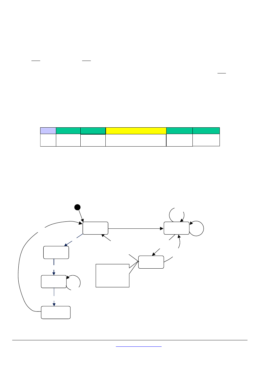
6 Appendix
6.1
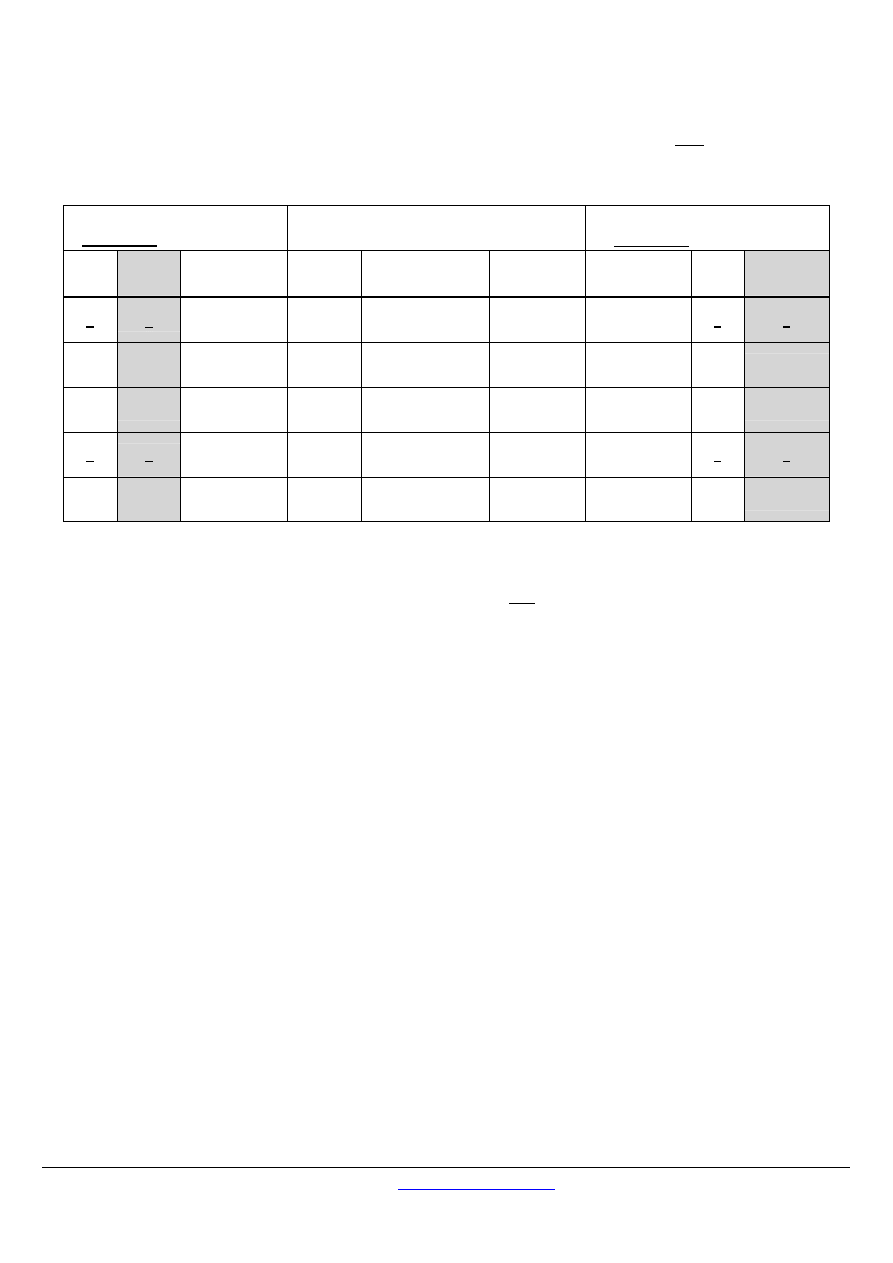
Appendix A - Management of Serial Line Diagnostic Counters
6.1.1 General
description
MODBUS Serial Line defines a list of diagnostic counters to allow performance and error management.
These counters are accessible using the MODBUS application protocol and its Diagnostic function (function code 08).
Each counter can be get by a sub-function code bound to the counter number. All counters can be cleared using the sub-function
code 0x0A.
The format of the Diagnostic function is described in the MODBUS application protocol specification.
Herein is the list of diagnostics and associated sub-function codes supported by a serial line device.
Sub-
function
code
Counter
number
Hex
Dec
Counters Name
Comments
(for diagram below)
0x0B
1
Return Bus Message Count
Quantity of messages that the remote device has detected on the
communications system since its last restart, clear counters operation,
or power–up. Messages with bad CRC are not taken into account.
0x0C
2
Return Bus Communication Error
Count
Quantity of CRC errors encountered by the remote device since its last
restart, clear counters operation, or power–up. In case of an error
detected on the character level, (overrun, parity error), or in case of a
message length < 3 bytes, the receiving device is not able to calculate
the CRC. In such cases, this counter is also incremented.
0x0D
3
Return Slave Exception Error Count
Quantity of MODBUS exception error detected by the remote device
since its last restart, clear counters operation, or power–up. It
comprises also the error detected in broadcast messages even if an
exception message is not returned in this case.
Exception errors are described and listed in "MODBUS Application
Protocol Specification" document.
0xOE
4
Return Slave Message Count
Quantity of messages addressed to the remote device, including
broadcast messages, that the remote device has processed since its
last restart, clear counters operation, or power–up.
0x0F
5
Return Slave No Response Count
Quantity of messages received by the remote device for which it
returned no response (neither a normal response nor an exception
response), since its last restart, clear counters operation, or power–up.
Then, this counter counts the number of broadcast messages it has
received.
0x10
6
Return Slave NAK Count
Quantity of messages addressed to the remote device for which it
returned a Negative Acknowledge (NAK) exception response, since its
last restart, clear counters operation, or power–up. Exception
responses are described and listed in "MODBUS Application Protocol
Specification" document
.
0x11
7
Return Slave Busy Count
Quantity of messages addressed to the remote device for which it
returned a Slave Device Busy exception response, since its last restart,
clear counters operation, or power–up. Exception responses are
described and listed in "MODBUS Application Protocol Specification"
document
0x12
8
Return Bus Character Overrun Count
Quantity of messages addressed to the remote device that it could not
handle due to a character overrun condition, since its last restart, clear
counters operation, or power–up. A character overrun is caused by data
characters arriving at the port faster than they can be stored, or by the
loss of a character due to a hardware malfunction.
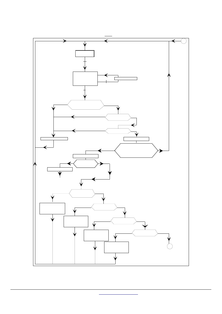
MODBUS over serial line specification and implementation guide V1.02
Modbus-IDA.ORG
Modbus.org
http://www.modbus.org/ 36/44
Dec 20, 2006
6.1.2
Counters Management Diagram
The following diagrams describe when each previous counters must be incremented.
3
Rest
reception
YES
NO
YES
NO
CRC incorrect
reception
255 characters
max
character error
3 characters silence
NO
YES
error on at least
1 frame character
length
< 3 bytes
slave
number 0
NO
1
YES
NO
length
incorrect
NO
addressing
incorrect
data
incorrect
2
exception
n° 3
CPT3 = CPT3 + 1
exception
n° 2
CPT3 = CPT3 + 1
exception
n° 3
CPT3 = CPT3 + 1
NO
NO
YES
YES
slave number
=
workstation slave
number
function code
not known
YES
YES
YES
NO
CPT8 = CPT8 + 1
CPT1 = CPT1 + 1
CPT2 = CPT2 + 1
CPT5 = CPT5 + 1
CPT4 = CPT4 + 1
exception
n° 1
CPT3 = CPT3 + 1
YES
character overrun
end of frame detected
CPT1 = CPT1 + 1
NO
YES
CPT4 = CPT4 + 1
CPT5 = CPT5 + 1
slave number
= 0
NO
reception max
number
characters
slave number = 0
or
slave number = my slave
number
IDLE
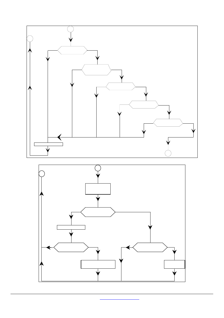
MODBUS over serial line specification and implementation guide V1.02
Modbus-IDA.ORG
Modbus.org
http://www.modbus.org/
37/44
Dec 20, 2006
3
YES
NO
function code
YES
NO
prohibited in
broadcasts
YES
NO
length
incorrect
YES
NO
addressing
incorrect
YES
NO
data
incorrect
2
CPT3 = CPT3 + 1
1
function code
not known
exception response
2
CPT3 = CPT3 + 1
application
processing
processing
error
NO
YES
broadcast
NO
YES
broadcast
NO
YES
response
3

MODBUS over serial line specification and implementation guide V1.02
Modbus-IDA.ORG
Modbus.org
http://www.modbus.org/ 38/44
Dec 20, 2006
6.2
Appendix B - LRC/CRC Generation
6.2.1 LRC
Generation
The Longitudinal Redundancy Checking (LRC) field is one byte, containing an 8–bit binary value. The LRC value is calculated by the
transmitting device, which appends the LRC to the message. The device that receives recalculates an LRC during receipt of the
message, and compares the calculated value to the actual value it received in the LRC field. If the two values are not equal, an error
results.
The LRC is calculated by adding together successive 8–bit bytes in the message, discarding any carries, and then two’s
complementing the result. The LRC is an 8–bit field, therefore each new addition of a character that would result in a value higher than
255 decimal simply ‘rolls over’ the field’s value through zero. Because there is no ninth bit, the carry is discarded automatically.
A procedure for generating an LRC is:
1.
Add all bytes in the message, excluding the starting ‘colon’ and ending CRLF. Add them into an 8–bit field, so that
carries will be discarded.
2.
Subtract the final field value from FF hex (all 1’s), to produce the ones–complement.
3.
Add 1 to produce the twos–complement.
Placing the LRC into the Message
When the 8–bit LRC (2 ASCII characters) is transmitted in the message, the high–order character will be transmitted first, followed by
the low–order character. For example, if the LRC value is 61 hex (0110 0001):
Colon
Addr
Func
Data
Count
Data
Data
Data
Data
LRC
Hi
CR
LF
LRC
Lo
"6" "1"
0x36 0x31
Figure 29:
LRC Character Sequence
Example: an example of a C language function performing LRC generation is shown below.
The function takes two arguments:
unsigned char *auchMsg;
A pointer to the message buffer containing binary data to be used for generating the LRC,
unsigned short usDataLen; The quantity of bytes in the message buffer.
LRC Generation Function
static unsigned char LRC(auchMsg, usDataLen)
/* the function returns the LRC as a type unsigned char */
unsigned char *auchMsg ;
/* message to calculate LRC upon */
unsigned short usDataLen ;
/* quantity of bytes in message */
{
unsigned char uchLRC = 0 ;
/* LRC char initialized */
while (usDataLen––)
/* pass through message buffer */
uchLRC += *auchMsg++ ;
/* add buffer byte without carry */
return ((unsigned char)(–((char)uchLRC))) ;
/* return twos complement */
}

MODBUS over serial line specification and implementation guide V1.02
Modbus-IDA.ORG
Modbus.org
http://www.modbus.org/
39/44
Dec 20, 2006
6.2.2 CRC
Generation
The Cyclical Redundancy Checking (CRC) field is two bytes, containing a 16–bit binary value. The CRC value is calculated by the
transmitting device, which appends the CRC to the message. The device that receives recalculates a CRC during receipt of the
message, and compares the calculated value to the actual value it received in the CRC field. If the two values are not equal, an error
results.
The CRC is started by first preloading a 16–bit register to all 1’s. Then a process begins of applying successive 8–bit bytes of the
message to the current contents of the register. Only the eight bits of data in each character are used for generating the CRC. Start
and stop bits and the parity bit, do not apply to the CRC.
During generation of the CRC, each 8–bit character is exclusive ORed with the register contents. Then the result is shifted in the
direction of the least significant bit (LSB), with a zero filled into the most significant bit (MSB) position. The LSB is extracted and
examined. If the LSB was a 1, the register is then exclusive ORed with a preset, fixed value. If the LSB was a 0, no exclusive OR takes
place.
This process is repeated until eight shifts have been performed. After the last (eighth) shift, the next 8–bit character is exclusive ORed
with the register’s current value, and the process repeats for eight more shifts as described above. The final content of the register,
after all the characters of the message have been applied, is the CRC value.
A procedure for generating a CRC is:
1. Load a 16–bit register with FFFF hex (all 1’s). Call this the CRC register.
2. Exclusive OR the first 8–bit byte of the message with the low–order byte of the 16–bit CRC register, putting the result in the
CRC register.
3. Shift the CRC register one bit to the right (toward the LSB), zero–filling the MSB. Extract and examine the LSB.
4. (If the LSB was 0): Repeat Step 3 (another shift).
(If the LSB was 1): Exclusive OR the CRC register with the polynomial value 0xA001 (1010 0000 0000 0001).
5. Repeat Steps 3 and 4 until 8 shifts have been performed. When this is done, a complete 8–bit byte will have been
processed.
6. Repeat Steps 2 through 5 for the next 8–bit byte of the message. Continue doing this until all bytes have been processed.
7. The final content of the CRC register is the CRC value.
8. When the CRC is placed into the message, its upper and lower bytes must be swapped as described below.
Placing the CRC into the Message
When the 16–bit CRC (two 8–bit bytes) is transmitted in the message, the low-order byte will be transmitted first, followed by the high-
order byte.
For example, if the CRC value is 1241 hex (0001 0010 0100 0001):
Addr
Func
Data
Count
Data
Data
Data
Data
CRC
Lo
CRC
Hi
0x41 0x12
Figure 30:
CRC Byte Sequence
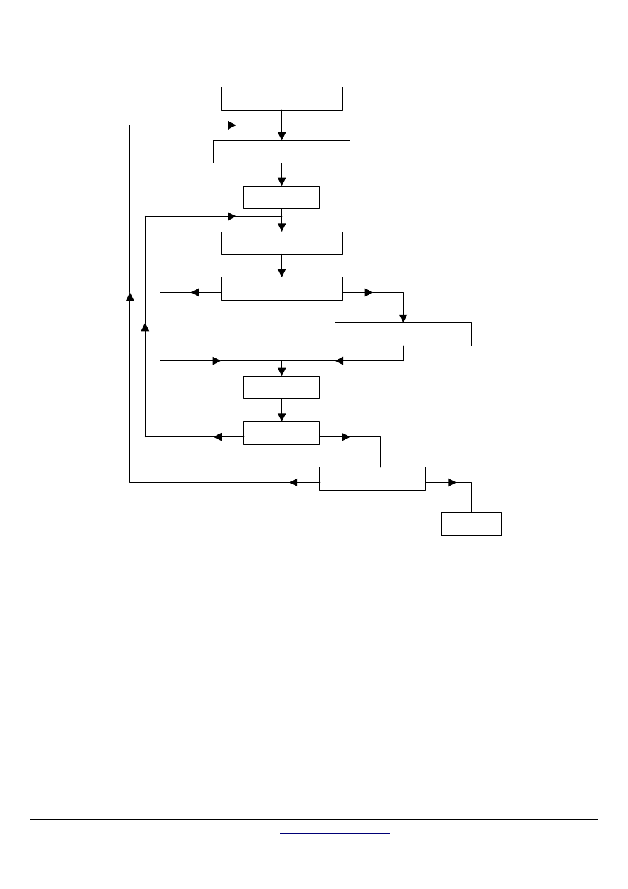
MODBUS over serial line specification and implementation guide V1.02
Modbus-IDA.ORG
Modbus.org
http://www.modbus.org/ 40/44
Dec 20, 2006
Calculation algorithm of the CRC 16
OxFFFF
→
CRC16
CRC16 XOR BYTE
→
CRC16
N = 0
Move to the right CRC16
Carry over
CRC16 XOR POLY
→
CRC 16
N = N + 1
N > 7
Yes
No
No
Yes
End of message
Yes
No
END
Following BYTE
XOR = exclusive or
N = number of information bits
POLY = calculation polynomial of the CRC 16 = 1010 0000 0000 0001
(Generating polynomial = 1 + x
2
+ x
15
+ x
16
)
In the CRC 16, the 1st byte transmitted is the least significant one.

MODBUS over serial line specification and implementation guide V1.02
Modbus-IDA.ORG
Modbus.org
http://www.modbus.org/
41/44
Dec 20, 2006
Example of CRC calculation (frame 02 07)
CRC register initialization
1111
1111
1111
1111
XOR 1st character
0000
0000
0000
0010
1111 1111 1111 1101
Move
1
0111
1111
1111
1110
|
1
Flag to 1, XOR polynomial
1010 0000 0000 0001
1101
1111
1111
1111
Move
2
0110
1111
1111
1111
|
1
Flag to 1, XOR polynomial
1010
0000
0000
0001
1100 1111 1111 1110
Move
3
0110
0111
1111
1111
0
Move
4
0011
0011
1111
1111
1
1010 0000 0000 0001
1001 0011 1111 1110
Move
5
0100
1001
1111
1111
0
Move
6
0010
0100
1111
1111
1
1010 0000 0000 0001
1000 0100 1111 1110
Move
7
0100
0010
0111
1111
0
Move
8
0010
0001
0011
1111
1
1010 0000 0000 0001
1000 0001 0011 1110
XOR 2nd character
0000 0000 0000 0111
1000
0001
0011
1001
Move
1
0100
0000
1001
1100
1
1010 0000 0000 0001
1110 0000 1001 1101
Move
2
0111
0000
0100
1110
1
1010 0000 0000 0001
1101 0000 0100 1111
Move
3
0110
1000
0010
0111
1
1010 0000 0000 0001
1100 1000 0010 0110
Move
4
0110
0100
0001
0011
0
Move
5
0011
0010
0000
1001
1
1010 0000 0000 0001
1001 0010 0000 1000
Move
6
0100
1001
0000
0100
0
Move
7
0010
0100
1000
0010
0
Move
8
0001
0010
0100
0001
0
Most significant
least significant
The CRC 16 of the frame is then: 4112

MODBUS over serial line specification and implementation guide V1.02
Modbus-IDA.ORG
Modbus.org
http://www.modbus.org/ 42/44
Dec 20, 2006
Example
An example of a C language function performing CRC generation is shown on the following pages. All of the possible CRC values are
preloaded into two arrays, which are simply indexed as the function increments through the message buffer. One array contains all of
the 256 possible CRC values for the high byte of the 16–bit CRC field, and the other array contains all of the values for the low byte.
Indexing the CRC in this way provides faster execution than would be achieved by calculating a new CRC value with each new
character from the message buffer.
Note: This function performs the swapping of the high/low CRC bytes internally. The bytes are already swapped in the CRC value that
is returned from the function.
Therefore the CRC value returned from the function can be directly placed into the message for transmission.
The function takes two arguments:
unsigned char *puchMsg;
A pointer to the message buffer containing binary data to be used for generating the CRC
unsigned short usDataLen;
The quantity of bytes in the message buffer.
CRC Generation Function
unsigned short CRC16 ( puchMsg, usDataLen )
/* The function returns the CRC as a unsigned short type */
unsigned char *puchMsg ;
/* message to calculate CRC upon
*/
unsigned short usDataLen ;
/* quantity of bytes in message
*/
{
unsigned char uchCRCHi = 0xFF ;
/* high byte of CRC initialized
*/
unsigned char uchCRCLo = 0xFF ;
/* low byte of CRC initialized
*/
unsigned uIndex ;
/* will index into CRC lookup table
*/
while (usDataLen--)
/* pass through message buffer
*/
{
uIndex = uchCRCLo ^ *puchMsg++ ;
/* calculate the CRC
*/
uchCRCLo = uchCRCHi ^ auchCRCHi[uIndex] ;
uchCRCHi = auchCRCLo[uIndex] ;
}
return (uchCRCHi << 8 | uchCRCLo) ;
}

MODBUS over serial line specification and implementation guide V1.02
Modbus-IDA.ORG
Modbus.org
http://www.modbus.org/
43/44
Dec 20, 2006
High-Order Byte Table
/* Table of CRC values for high–order byte */
static unsigned char auchCRCHi[] = {
0x00, 0xC1, 0x81, 0x40, 0x01, 0xC0, 0x80, 0x41, 0x01, 0xC0, 0x80, 0x41, 0x00, 0xC1, 0x81,
0x40, 0x01, 0xC0, 0x80, 0x41, 0x00, 0xC1, 0x81, 0x40, 0x00, 0xC1, 0x81, 0x40, 0x01, 0xC0,
0x80, 0x41, 0x01, 0xC0, 0x80, 0x41, 0x00, 0xC1, 0x81, 0x40, 0x00, 0xC1, 0x81, 0x40, 0x01,
0xC0, 0x80, 0x41, 0x00, 0xC1, 0x81, 0x40, 0x01, 0xC0, 0x80, 0x41, 0x01, 0xC0, 0x80, 0x41,
0x00, 0xC1, 0x81, 0x40, 0x01, 0xC0, 0x80, 0x41, 0x00, 0xC1, 0x81, 0x40, 0x00, 0xC1, 0x81,
0x40, 0x01, 0xC0, 0x80, 0x41, 0x00, 0xC1, 0x81, 0x40, 0x01, 0xC0, 0x80, 0x41, 0x01, 0xC0,
0x80, 0x41, 0x00, 0xC1, 0x81, 0x40, 0x00, 0xC1, 0x81, 0x40, 0x01, 0xC0, 0x80, 0x41, 0x01,
0xC0, 0x80, 0x41, 0x00, 0xC1, 0x81, 0x40, 0x01, 0xC0, 0x80, 0x41, 0x00, 0xC1, 0x81, 0x40,
0x00, 0xC1, 0x81, 0x40, 0x01, 0xC0, 0x80, 0x41, 0x01, 0xC0, 0x80, 0x41, 0x00, 0xC1, 0x81,
0x40, 0x00, 0xC1, 0x81, 0x40, 0x01, 0xC0, 0x80, 0x41, 0x00, 0xC1, 0x81, 0x40, 0x01, 0xC0,
0x80, 0x41, 0x01, 0xC0, 0x80, 0x41, 0x00, 0xC1, 0x81, 0x40, 0x00, 0xC1, 0x81, 0x40, 0x01,
0xC0, 0x80, 0x41, 0x01, 0xC0, 0x80, 0x41, 0x00, 0xC1, 0x81, 0x40, 0x01, 0xC0, 0x80, 0x41,
0x00, 0xC1, 0x81, 0x40, 0x00, 0xC1, 0x81, 0x40, 0x01, 0xC0, 0x80, 0x41, 0x00, 0xC1, 0x81,
0x40, 0x01, 0xC0, 0x80, 0x41, 0x01, 0xC0, 0x80, 0x41, 0x00, 0xC1, 0x81, 0x40, 0x01, 0xC0,
0x80, 0x41, 0x00, 0xC1, 0x81, 0x40, 0x00, 0xC1, 0x81, 0x40, 0x01, 0xC0, 0x80, 0x41, 0x01,
0xC0, 0x80, 0x41, 0x00, 0xC1, 0x81, 0x40, 0x00, 0xC1, 0x81, 0x40, 0x01, 0xC0, 0x80, 0x41,
0x00, 0xC1, 0x81, 0x40, 0x01, 0xC0, 0x80, 0x41, 0x01, 0xC0, 0x80, 0x41, 0x00, 0xC1, 0x81,
0x40
} ;
Low-Order Byte Table
/* Table of CRC values for low–order byte */
static char auchCRCLo[] = {
0x00, 0xC0, 0xC1, 0x01, 0xC3, 0x03, 0x02, 0xC2, 0xC6, 0x06, 0x07, 0xC7, 0x05, 0xC5, 0xC4,
0x04, 0xCC, 0x0C, 0x0D, 0xCD, 0x0F, 0xCF, 0xCE, 0x0E, 0x0A, 0xCA, 0xCB, 0x0B, 0xC9, 0x09,
0x08, 0xC8, 0xD8, 0x18, 0x19, 0xD9, 0x1B, 0xDB, 0xDA, 0x1A, 0x1E, 0xDE, 0xDF, 0x1F, 0xDD,
0x1D, 0x1C, 0xDC, 0x14, 0xD4, 0xD5, 0x15, 0xD7, 0x17, 0x16, 0xD6, 0xD2, 0x12, 0x13, 0xD3,
0x11, 0xD1, 0xD0, 0x10, 0xF0, 0x30, 0x31, 0xF1, 0x33, 0xF3, 0xF2, 0x32, 0x36, 0xF6, 0xF7,
0x37, 0xF5, 0x35, 0x34, 0xF4, 0x3C, 0xFC, 0xFD, 0x3D, 0xFF, 0x3F, 0x3E, 0xFE, 0xFA, 0x3A,
0x3B, 0xFB, 0x39, 0xF9, 0xF8, 0x38, 0x28, 0xE8, 0xE9, 0x29, 0xEB, 0x2B, 0x2A, 0xEA, 0xEE,
0x2E, 0x2F, 0xEF, 0x2D, 0xED, 0xEC, 0x2C, 0xE4, 0x24, 0x25, 0xE5, 0x27, 0xE7, 0xE6, 0x26,
0x22, 0xE2, 0xE3, 0x23, 0xE1, 0x21, 0x20, 0xE0, 0xA0, 0x60, 0x61, 0xA1, 0x63, 0xA3, 0xA2,
0x62, 0x66, 0xA6, 0xA7, 0x67, 0xA5, 0x65, 0x64, 0xA4, 0x6C, 0xAC, 0xAD, 0x6D, 0xAF, 0x6F,
0x6E, 0xAE, 0xAA, 0x6A, 0x6B, 0xAB, 0x69, 0xA9, 0xA8, 0x68, 0x78, 0xB8, 0xB9, 0x79, 0xBB,
0x7B, 0x7A, 0xBA, 0xBE, 0x7E, 0x7F, 0xBF, 0x7D, 0xBD, 0xBC, 0x7C, 0xB4, 0x74, 0x75, 0xB5,
0x77, 0xB7, 0xB6, 0x76, 0x72, 0xB2, 0xB3, 0x73, 0xB1, 0x71, 0x70, 0xB0, 0x50, 0x90, 0x91,
0x51, 0x93, 0x53, 0x52, 0x92, 0x96, 0x56, 0x57, 0x97, 0x55, 0x95, 0x94, 0x54, 0x9C, 0x5C,
0x5D, 0x9D, 0x5F, 0x9F, 0x9E, 0x5E, 0x5A, 0x9A, 0x9B, 0x5B, 0x99, 0x59, 0x58, 0x98, 0x88,
0x48, 0x49, 0x89, 0x4B, 0x8B, 0x8A, 0x4A, 0x4E, 0x8E, 0x8F, 0x4F, 0x8D, 0x4D, 0x4C, 0x8C,
0x44, 0x84, 0x85, 0x45, 0x87, 0x47, 0x46, 0x86, 0x82, 0x42, 0x43, 0x83, 0x41, 0x81, 0x80,
0x40
};

MODBUS over serial line specification and implementation guide V1.02
Modbus-IDA.ORG
Modbus.org
http://www.modbus.org/ 44/44
Dec 20, 2006
6.3
Appendix E - References
ANSI/ TIA/ EIA-232-F-1997
Interface Between Data Terminal Equipment and Data Circuit-Terminating Equipment
Employing Serial Binary Data Interchange.
ANSI/ TIA/ EIA-485-A-1998
Electrical Characteristics of Generators and Receivers for Use in Balanced Digital Multipoint
Systems.
AWG "American Wire Gauge" is a standard method denoting wire diameter, it is used in the USA
and in other countries; increasing gauge numbers give decreasing wire parameters.
See for example D.G. Fink and H.W. Beaty, Standard Handbook for Electrical Engineers,
13th Edition, McGraw-Hill, 1993.
MODBUS.org
MODBUS application protocol specification
Document Outline
- Introduction
- MODBUS Data Link Layer
- Physical Layer
- Installation and Documentation
- Implementation Classes
- Appendix
Wyszukiwarka
Podobne podstrony:
egzamin v1 02 1
Denise A Agnew Special Investigations Agency Over The Line (Ellora s Cave)
podstawy teorii part one bzz v1 07 02 06
poprawkowe, MAD ep 13 02 2002 v1
podstawy teorii part two bzz v1 07 02 06
02 06 Roboty na dachach v1 1
SKO1 e 02 2006 v1
02 Prace na wysokosci v1 1
06-02-Roboty w kanalach studniach studzienkach v1 1
02 02 Rusztowania v1 1
MODBUS Application Protocol V1 1b
podstawy teorii part three bzz v1 07 02 06
05 02 Organizacja ruchu na budowie liniowej v1 1
podstawy teorii part one bzz v1 07 02 06
Dennis Wheatley [Roger Brook 02] The Shadow of Tyburn Tree(v1 5)(rtf)
Forgotten Realms Abolethic Sovereignty, 02 Bruce R Cordell City of Torment v1 [rtf]
więcej podobnych podstron