
Jul/Aug 2002 13
8900 Marybank Dr
Austin, TX 78750
A Software-Defined Radio
for the Masses, Part 1
By Gerald Youngblood, AC5OG
This series describes a complete PC
-based, software-defined
radio that uses a sound card and an innovative detector
circuit. Mathematics is minimized in the
explanation. Come see how it
’s done.
A
certain convergence occurs
when multiple technologies
align in time to make possible
those things that once were only
dreamed. The explosive growth of the
Internet starting in 1994 was one of
those events. While the Internet had
existed for many years in government
and education prior to that, its popu-
larity had never crossed over into the
general populace because of its slow
speed and arcane interface. The devel-
opment of the Web browser, the
rapidly accelerating power and avail-
ability of the PC, and the availability
of inexpensive and increasingly
speedy modems brought about the
Internet convergence. Suddenly, it all
came together so that the Internet and
the worldwide Web joined the every-
day lexicon of our society.
A similar convergence is occurring
in radio communications through digi-
tal signal processing (DSP) software to
perform most radio functions at per-
formance levels previously considered
unattainable. DSP has now been
incorporated into much of the ama-
teur radio gear on the market to de-
liver improved noise-reduction and
digital-filtering performance. More
recently, there has been a lot of discus-
sion about the emergence of so-called
software-defined radios (SDRs).
A software-defined radio is charac-
terized by its flexibility: Simply modi-
fying or replacing software programs
can completely change its functional-
ity. This allows easy upgrade to new
modes and improved performance
without the need to replace hardware.
SDRs can also be easily modified to
accommodate the operating needs of
individual applications. There is a dis-
tinct difference between a radio that
internally uses software for some of its
functions and a radio that can be com-
pletely redefined in the field through
modification of software. The latter is
a software-defined radio.
This SDR convergence is occurring
because of advances in software and
silicon that allow digital processing of
radio-frequency signals. Many of
these designs incorporate mathemati-
cal functions into hardware to perform
all of the digitization, frequency selec-
tion, and down-conversion to base-

14 Jul/Aug 2002
band. Such systems can be quite com-
plex and somewhat out of reach to
most amateurs.
One problem has been that unless
you are a math wizard and proficient
in programming C++ or assembly lan-
guage, you are out of luck. Each can be
somewhat daunting to the amateur as
well as to many professionals. Two
years ago, I set out to attack this chal-
lenge armed with a fascination for
technology and a 25-year-old, virtu-
ally unused electrical engineering de-
gree. I had studied most of the math in
college and even some of the signal
processing theory, but 25 years is a
long time. I found that it really was a
challenge to learn many of the disci-
plines required because much of the
literature was written from a math-
ematician’s perspective.
Now that I am beginning to grasp
many of the concepts involved in soft-
ware radios, I want to share with the
Amateur Radio community what I
have learned without using much
more than simple mathematical con-
cepts. Further, a software radio
should have as little hardware as pos-
sible. If you have a PC with a sound
card, you already have most of the
required hardware. With as few as
three integrated circuits you can be up
and running with a Tayloe detector—
an innovative, yet simple, direct-con-
version receiver. With less than a
dozen chips, you can build a trans-
ceiver that will outperform much of
the commercial gear on the market.
Approach the Theory
In this article series, I have chosen to
focus on practical implementation
rather than on detailed theory. There
are basic facts that must be understood
to build a software radio. However,
much like working with integrated cir-
cuits, you don’t have to know how to
create the IC in order to use it in a de-
sign. The convention I have chosen is to
describe practical applications fol-
lowed by references where appropriate
for more detailed study. One of the
easier to comprehend references I have
found is The Scientist and Engineer’s
Guide to Digital Signal Processing by
Steven W. Smith. It is free for download
over the Internet at
. I consider it required reading for
those who want to dig deeper into
implementation as well as theory. I will
refer to it as the “DSP Guide” many
times in this article series for further
study.
So get out your four-function calcu-
lator (okay, maybe you need six or
seven functions) and let’s get started.
But first, let’s set forth the objectives
of the complete SDR design:
• Keep the math simple
• Use a sound-card equipped PC to pro-
vide all signal-processing functions
• Program the user interface and all
signal-processing algorithms in
Visual Basic for easy development
and maintenance
• Utilize the Intel Signal Processing
Library for core DSP routines to
minimize the technical knowledge
requirement and development time,
and to maximize performance
• Integrate a direct conversion (D-C)
receiver for hardware design sim-
plicity and wide dynamic range
• Incorporate direct digital synthesis
(DDS) to allow flexible frequency
control
• Include transmit capabilities using
similar techniques as those used in
the D-C receiver.
Analog and Digital Signals in
the Time Domain
To understand DSP we first need to
understand the relationship between
digital signals and their analog coun-
terparts. If we look at a 1-V (pk) sine
wave on an analog oscilloscope, we see
that the signal makes a perfectly
smooth curve on the scope, no matter
how fast the sweep frequency. In fact,
if it were possible to build a scope with
an infinitely fast horizontal sweep, it
would still display a perfectly smooth
curve (really a straight line at that
point). As such, it is often called a con-
tinuous-time signal since it is continu-
ous in time. In other words, there are
an infinite number of different volt-
ages along the curve, as can be seen on
the analog oscilloscope trace.
On the other hand, if we were to
measure the same sine wave with a
digital voltmeter at a sampling rate of
four times the frequency of the sine
wave, starting at time equals zero, we
would read: 0 V at 0°, 1 V at 90°, 0 V at
180° and –1 V at 270° over one com-
plete cycle. The signal could continue
perpetually, and we would still read
those same four voltages over and
again, forever. We have measured the
voltage of the signal at discrete mo-
ments in time. The resulting voltage-
measurement sequence is therefore
called a discrete-time signal.
If we save each discrete-time signal
voltage in a computer memory and we
know the frequency at which we
sampled the signal, we have a discrete-
time sampled signal. This is what an
analog-to-digital converter (ADC)
does. It uses a sampling clock to mea-
sure discrete samples of an incoming
analog signal at precise times, and it
produces a digital representation of
the input sample voltage.
In 1933, Harry Nyquist discovered
that to accurately recover all the com-
ponents of a periodic waveform, it is
necessary to use a sampling frequency
of at least twice the bandwidth of the
signal being measured. That mini-
mum sampling frequency is called the
Nyquist criterion. This may be ex-
pressed as:
bw
s
2 f
f
≥
(Eq 1)
where f
s
is the sampling rate and f
bw
is
the bandwidth. See? The math isn’t so
bad, is it?
Now as an example of the Nyquist
criterion, let’s consider human hear-
ing, which typically ranges from 20 Hz
to 20 kHz. To recreate this frequency
response, a CD player must sample at
a frequency of at least 40 kHz. As we
will soon learn, the maximum fre-
quency component must be limited to
20 kHz through low-pass filtering to
prevent distortion caused by false im-
ages of the signal. To ease filter re-
quirements, therefore, CD players use
a standard sampling rate of 44,100 Hz.
All modern PC sound cards support
that sampling rate.
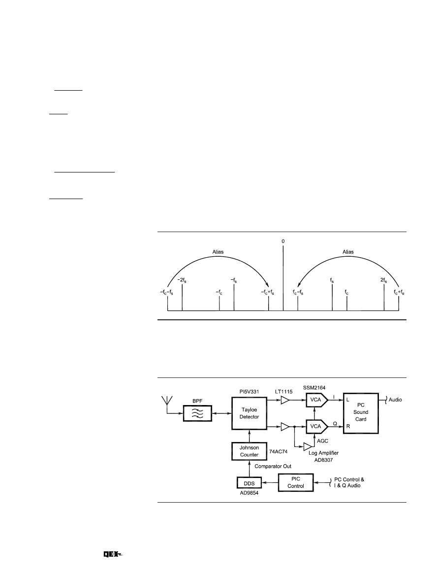
What happens if the sampled band-
width is greater than half the sampling
rate and is not limited by a low-pass
filter? An alias of the signal is produced
that appears in the output along with
the original signal. Aliases can cause
distortion, beat notes and unwanted
spurious images. Fortunately, alias
frequencies can be precisely predicted
and prevented with proper low-pass or
band-pass filters, which are often re-
ferred to as anti-aliasing filters, as
shown in Fig 1. There are even cases
where the alias frequency can be used
to advantage; that will be discussed
later in the article.
This is the point where most texts
on DSP go into great detail about what
sampled signals look like above the
Nyquist frequency. Since the goal of
this article is practical implementa-
tion, I refer you to Chapter 3 of the
DSP Guide for a more in-depth discus-
sion of sampling, aliases, A-to-D and
Fig 1—A/D conversion with antialiasing
low-pass filter.
Jul/Aug 2002 15
D-to-A conversion. Also refer to Doug Smith’s article, “Sig-
nals, Samples, and Stuff: A DSP Tutorial.”
What you need to know for now is that if we adhere to the
, we can accurately sample, pro-
cess and recreate virtually any desired waveform. The
sampled signal will consist of a series of numbers in com-
puter memory measured at time intervals equal to the
sampling rate. Since we now know the amplitude of the
signal at discrete time intervals, we can process the digi-
tized signal in software with a precision and flexibility not
possible with analog circuits.
From RF to a PC’s Sound Card
Our objective is to convert a modulated radio-frequency
signal from the frequency domain to the time domain for
software processing. In the frequency domain, we measure
amplitude versus frequency (as with a spectrum analyzer);
in the time domain, we measure amplitude versus time (as
with an oscilloscope).
In this application, we choose to use a standard 16-bit PC
sound card that has a maximum sampling rate of
44,100 Hz. According to
, this means that the maxi-
mum-bandwidth signal we can accommodate is 22,050 Hz.
With quadrature sampling, discussed later, this can actu-
ally be extended to 44 kHz. Most sound cards have built-in
antialiasing filters that cut off sharply at around 20 kHz.
(For a couple hundred dollars more, PC sound cards are
now available that support 24 bits at a 96-kHz sampling
rate with up to 105 dB of dynamic range.)
Most commercial and amateur DSP designs use dedicated
DSPs that sample intermediate frequencies (IFs) of 40 kHz
or above. They use traditional analog superheterodyne tech-
niques for down-conversion and filtering. With the advent of
very-high-speed and wide-bandwidth ADCs, it is now pos-
sible to directly sample signals up through the entire HF
range and even into the low VHF range. For example, the
Analog Devices AD9430 A/D converter is specified with
sample rates up to 210 Msps at 12 bits of resolution and a
700-MHz bandwidth. That 700-MHz bandwidth can be used
in under-sampling applications, a topic that is beyond the
scope of this article series.
The goal of my project is to build a PC-based software-
defined radio that uses as little external hardware as pos-
sible while maximizing dynamic range and flexibility. To
do so, we will need to convert the RF signal to audio fre-
quencies in a way that allows removal of the unwanted
mixing products or images caused by the down-conversion
process. The simplest way to accomplish this while main-
taining wide dynamic range is to use D-C techniques to
translate the modulated RF signal directly to baseband.
We can mix the signal with an oscillator tuned to the RF
carrier frequency to translate the bandwidth-limited sig-
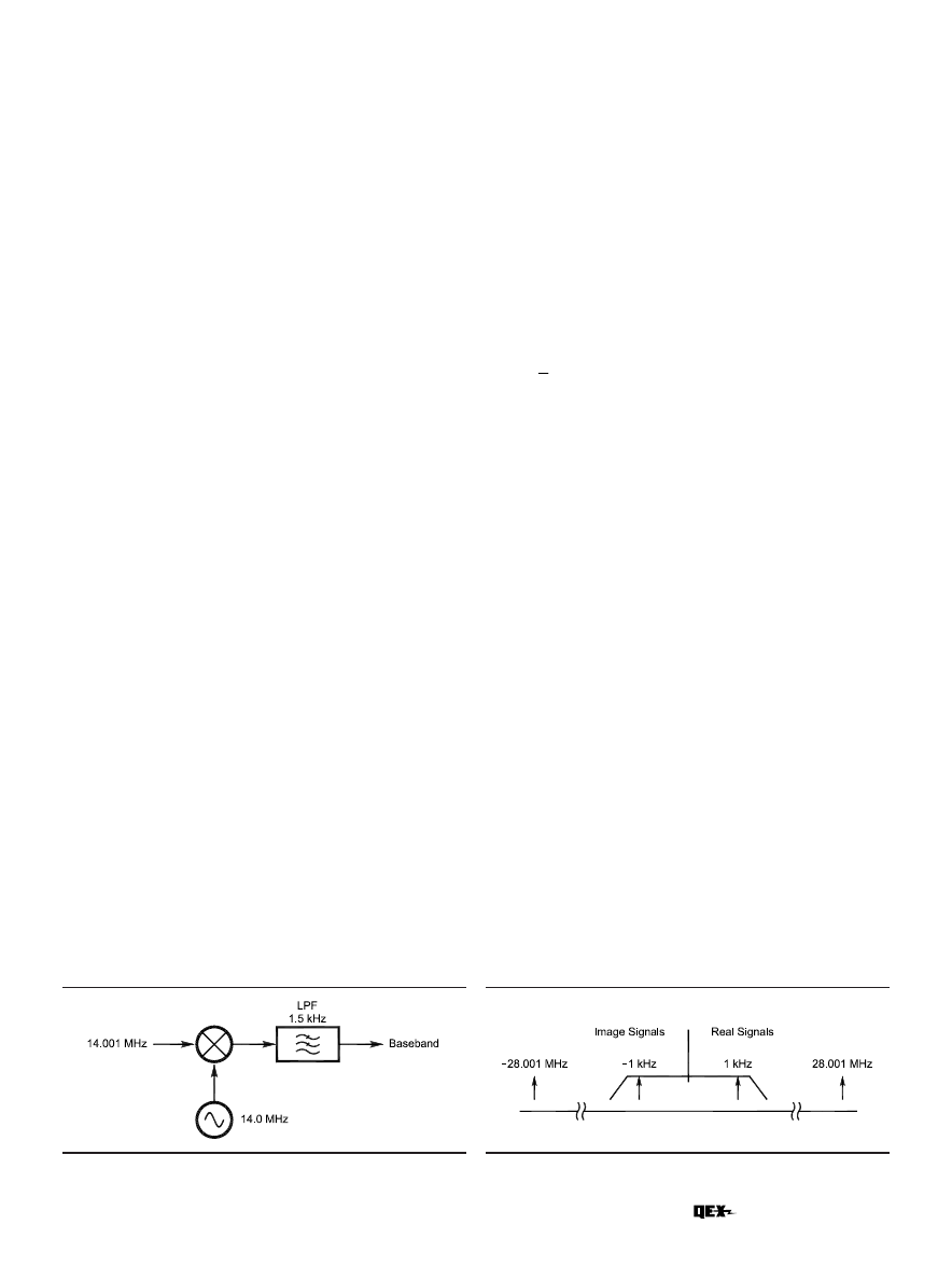
nal to a 0-Hz IF as shown in Fig 2.
The example in the figure shows a 14.001-MHz carrier
signal mixed with a 14.000-MHz local oscillator to translate
the carrier to 1 kHz. If the low-pass filter had a cutoff of
1.5 kHz, any signal between 14.000 MHz and 14.0015 MHz
would be within the passband of the direct-conversion re-
ceiver. The problem with this simple approach is that we
would also simultaneously receive all signals between
13.9985 MHz and 14.000 MHz as unwanted images within
the passband, as illustrated in Fig 3. Why is that?
Most amateurs are familiar with the concept of sum and
difference frequencies that result from mixing two signals.
When a carrier frequency, f
c
, is mixed with a local oscilla-
tor, f
lo
, they combine in the general form:
[
]
)
(
)
(
2
1
lo
c
lo
c
lo
c
f
f
f
f
f
f
−
+
+
=
MHz
001
.
0
MHz
000
.
14
MHz
001
.
14
MHz
001
.
28
MHz
000
.
14
MHz
001
.
14
lo
c
lo
c
=
−
=
−
=
+
=
+
f
f
f
f
MHz
001
.
0
MHz
000
.
14
MHz
001
.
14
lo
c
−
=
+
−
=
+
−
f
f
(Eq 2)
When we use the direct-conversion mixer shown in Fig 2,
we will receive these primary output signals:
Note that we also receive the image frequency that “folds
over” the primary output signals:
A low-pass filter easily removes the 28.001-MHz sum
frequency, but the –0.001-MHz difference-frequency image
will remain in the output. This unwanted image is the
lower sideband with respect to the 14.000-MHz carrier fre-
quency. This would not be a problem if there were no sig-
nals below 14.000 MHz to interfere. As previously stated,
all undesired signals between 13.9985 and 14.000 MHz will
translate into the passband along with the desired signals
above 14.000 MHz. The image also results in increased
noise in the output.
So how can we remove the image-frequency signals? It
can be accomplished through quadrature mixing. Phasing
or quadrature transmitters and receivers—also called
Weaver-method or image-rejection mixers—have existed
since the early days of single sideband. In fact, my first
SSB transmitter was a used Central Electronics 20A ex-
citer that incorporated a phasing design. Phasing systems
lost favor in the early 1960s with the advent of relatively
inexpensive, high-performance filters.
To achieve good opposite-sideband or image suppression,
phasing systems require a precise balance of amplitude and
phase between two samples of the signal that are 90° out
1
.
Fig 2—A direct-conversion real mixer with a 1.5-kHz low-pass
filter.
Fig 3—Output spectrum of a real mixer illustrating the sum,
difference and image frequencies.
16 Jul/Aug 2002
of phase or in quadrature with each
other—“orthogonal” is the term used
in some texts. Until the advent of digi-
tal signal processing, it was difficult
to realize the level of image rejection
performance required of modern radio
systems in phasing designs. Since
digital signal processing allows pre-
cise numerical control of phase and
amplitude, quadrature modulation
and demodulation are the preferred
methods. Such signals in quadrature
allow virtually any modulation
method to be implemented in software
using DSP techniques.
Give Me I and Q and I Can
Demodulate Anything
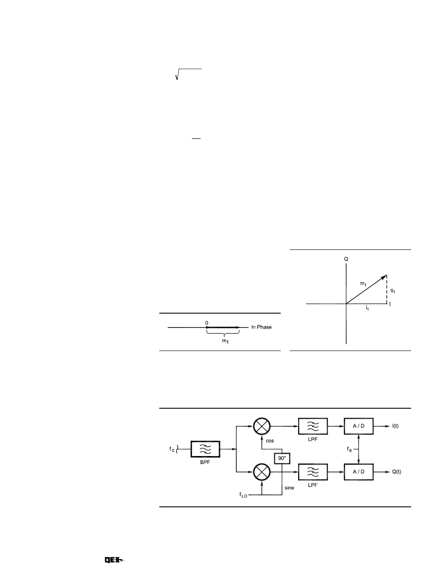
First, consider the direct-conversion
mixer shown in
nal is converted to baseband audio us-
ing a single channel, we can visualize
the output as varying in amplitude
along a single axis as illustrated in
Fig 4. We will refer to this as the in-
phase or I signal. Notice that its magni-
tude varies from a positive value to a
negative value at the frequency of the
modulating signal. If we use a diode to
rectify the signal, we would have cre-
ated a simple envelope or AM detector.
Remember that in AM envelope de-
tection, both modulation sidebands
carry information energy and both are
desired at the output. Only amplitude
information is required to fully de-
modulate the original signal. The
problem is that most other modulation
techniques require that the phase of
the signal be known. This is where
quadrature detection comes in. If we
delay a copy of the RF carrier by 90° to
form a quadrature (Q) signal, we can
then use it in conjunction with the
original in-phase signal and the math
we learned in middle school to deter-
mine the instantaneous phase and
amplitude of the original signal.
Fig 5 illustrates an RF carrier with
the level of the I signal plotted on the
x-axis and that of the Q signal plotted
on the y-axis of a plane. This is often
referred to in the literature as a
phasor diagram in the complex plane.
We are now able to extrapolate the two
signals to draw an arrow or phasor
that represents the instantaneous
magnitude and phase of the original
signal.
Okay, here is where you will have to
use a couple of those extra functions
on the calculator. To compute the
magnitude m
t
or envelope of the sig-
nal, we use the geometry of right tri-
angles. In a right triangle, the square
of the hypotenuse is equal to the sum
Fig 4—An in-phase signal (
I) on the real
plane. The magnitude,
m
(t)
, is easily
measured as the instantaneous peak
voltage, but no phase information is
available from in-phase detection. This is
the way an AM envelope detector works.
Fig 6—Quadrature sampling mixer: The RF carrier,
f
c
,
is fed to parallel mixers. The local
oscillator (Sine) is fed to the lower-channel mixer directly and is delayed by 90° (Cosine)
to feed the upper-channel mixer. The low-pass filters provide antialias filtering before
analog-to-digital conversion. The upper channel provides the in-phase (
I
(t)
) signal and the
lower channel provides the quadrature (
Q
(t)
) signal. In the PC SDR the low-pass filters
and A/D converters are integrated on the PC sound card.
Fig 5—I +
jQ are shown on the complex
plane. The vector rotates counterclock-
wise at a rate of 2
πππππf
c
. The magnitude and
phase of the rotating vector at any instant
in time may be determined through Eqs 3
and 4.
of the squares of the other two sides—
according to the Pythagorean theo-
rem. Or restating, the hypotenuse as
m
t
(magnitude with respect to time):
2
t
2
t
t
Q
I
m
+
=
(Eq 3)
The instantaneous phase of the sig-
nal as measured counterclockwise
from the positive I axis and may be
computed by the inverse tangent (or
arctangent) as follows:
=
−
t
t
1
t
tan
I
Q
φ
(Eq 4)
Therefore, if we measured the in-
stantaneous values of I and Q, we
would know everything we needed to
know about the signal at a given mo-
ment in time. This is true whether we
are dealing with continuous analog
signals or discrete sampled signals.
With I and Q, we can demodulate AM
signals directly using Eq 3 and FM
signals using Eq 4. To demodulate
SSB takes one more step. Quadrature
signals can be used analytically to re-
move the image frequencies and leave
only the desired sideband.
The mathematical equations for
quadrature signals are difficult but
are very understandable with a little
study.
I highly recommend that you
read the online article, “Quadrature
Signals: Complex, But Not Compli-
cated,” by Richard Lyons. It can be
found at
. The article de-
velops in a very logical manner how
quadrature-sampling I/Q demodula-
tion is accomplished. A basic under-
standing of these concepts is essential
to designing software-defined radios.
We can take advantage of the ana-
lytic capabilities of quadrature signals
through a quadrature mixer. To under-
stand the basic concepts of quadrature
mixing, refer to Fig 6, which illustrates
a quadrature-sampling I/Q mixer.
First, the RF input signal is band-
pass filtered and applied to the two
parallel mixer channels. By delaying
the local oscillator wave by 90°, we can
generate a cosine wave that, in tandem,
forms a quadrature oscillator. The RF
carrier, f
c
(t), is mixed with the respec-
tive cosine and sine wave local oscilla-
tors and is subsequently low-pass
filtered to create the in-phase, I(t), and
quadrature, Q(t), signals. The Q(t)
Jul/Aug 2002 17
channel is phase-shifted 90° relative to
the I(t) channel through mixing with
the sine local oscillator. The low-pass
filter is designed for cutoff below the
Nyquist frequency to prevent aliasing
in the A/D step. The A/D converts con-
tinuous-time signals to discrete-time
sampled signals. Now that we have the
I and Q samples in memory, we can
perform the magic of digital signal pro-
cessing.
Before we go further, let me reiter-
ate that one of the problems with this
method of down-conversion is that it
can be costly to get good opposite-side-
band suppression with analog circuits.
Any variance in component values will
cause phase or amplitude imbalance
between two channels, resulting in a
corresponding decrease in opposite-
sideband suppression. With analog
circuits, it is difficult to achieve better
than 40 dB of suppression without
much higher cost. Fortunately, it is
straightforward to correct the analog
imbalances in software.
Another significant drawback of di-
rect-conversion receivers is that the
noise increases as the demodulated sig-
nal approaches 0 Hz. Noise contribu-
tions come from a number of sources,
such as 1/f noise from the semiconduc-
tor devices themselves, 60-Hz and
120-Hz line noise or hum, microphonic
mechanical noise and local-oscillator
phase noise near the carrier frequency.
This can limit sensitivity since most
people prefer their CW tones to be be-
low 1 kHz. It turns out that most of
the low-frequency noise rolls off above
1 kHz. Since a sound card can process
signals all the way up to 20 kHz, why
not use some of that bandwidth to move
away from the low frequency noise? The
PC SDR uses an 11.025-kHz, offset-
baseband IF to reduce the noise to a
manageable level. By offsetting the
local oscillator by 11.025 kHz, we can
now receive signals near the carrier
frequency without any of the low-
frequency noise issues. This also
significantly reduces the effects of lo-
cal-oscillator phase noise. Once we
have digitally captured the signal, it is
a trivial software task to shift the de-
modulated signal down to a 0-Hz offset.
DSP in the Frequency Domain
Every DSP text I have read thus far
concentrates on time-domain filtering
and demodulation of SSB signals us-
ing finite-impulse-response (FIR) fil-
ters. Since these techniques have been
thoroughly discussed in the litera-
ture
,
my PC SDR, they will not be covered
in this article series.
My PC SDR uses the power of the
fast Fourier transform (FFT) to do al-
most all of the heavy lifting in the fre-
quency domain. Most DSP texts use a
lot of ink to derive the math so that one
can write the FFT code. Since Intel has
so helpfully provided the code in ex-
ecutable form in their signal-process-
ing library,
an FFT: We just need to know how to
use it. Simply put, the FFT converts
the complex I and Q discrete-time sig-
nals into the frequency domain. The
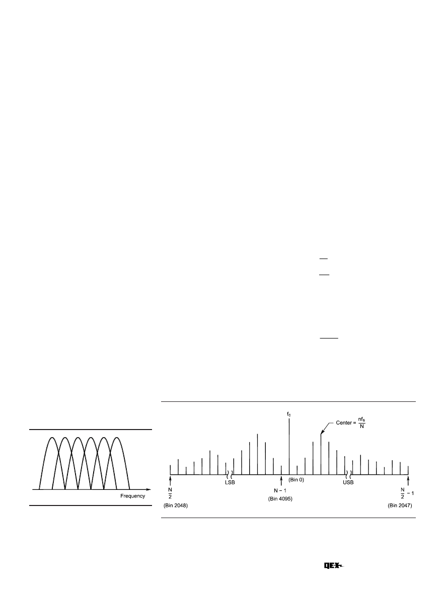
FFT output can be thought of as a
large bank of very narrow band-pass
filters, called bins, each one measur-
ing the spectral energy within its
respective bandwidth. The output re-
sembles a comb filter wherein each bin
slightly overlaps its adjacent bins
forming a scalloped curve, as shown in
Fig 7. When a signal is precisely at the
center frequency of a bin, there will be
a corresponding value only in that bin.
As the frequency is offset from the
bin’s center, there will be a corre-
sponding increase in the value of the
adjacent bin and a decrease in the
value of the current bin. Mathemati-
cal analysis fully describes the rela-
tionship between FFT bins,
is beyond the scope of this article.
Further, the FFT allows us to mea-
sure both phase and amplitude of the
signal within each bin using
and
above. The complex version allows us
to measure positive and negative fre-
quencies separately. Fig 8 illustrates
the output of a complex, or quadra-
ture, FFT.
The bandwidth of each FFT bin may
be computed as shown in Eq 5, where
BW
bin
is the bandwidth of a single bin,
f
s
is the sampling rate and N is the size
of the FFT. The center frequency of
each FFT bin may be determined by
Eq 6 where f
center
is the bin’s center
frequency, n is the bin number, f
s
is the
sampling rate and N is the size of the
FFT. Bins zero through (N/2)–1 repre-
sent upper-sideband frequencies and
bins N/2 to N–1 represent lower-side-
band frequencies around the carrier
frequency.
N
f
BW
s
bin
=
(Eq 5)
N
nf
f
s
center
=
(Eq 6)
If we assume the sampling rate of
the sound card is 44.1 kHz and the
number of FFT bins is 4096, then the
bandwidth and center frequency of
each bin would be:
and
Hz
7666
.
10
4096
44100
bin
=
=
BW
Hz
7666
.
10
center
n
f
=
Fig 7—FFT output resembles a comb filter:
Each bin of the FFT overlaps its adjacent
bins just as in a comb filter. The 3-dB
points overlap to provide linear output. The
phase and magnitude of the signal in each
bin is easily determined mathematically
with
Fig 8—Complex FFT output: The output of a complex FFT may be thought of as a series
of band-pass filters aligned around the carrier frequency,
f
c
, at bin 0.
N represents the
number of FFT bins. The upper sideband is located in bins 1 through
(N/2)–1 and the
lower sideband is located in bins
N/2 to N–1. The center frequency and bandwidth of
each bin may be calculated using Eqs 5 and 6.
What this all means is that the
receiver will have 4096, ~11-Hz-wide
18 Jul/Aug 2002
band-pass filters. We can therefore
create band-pass filters from 11 Hz to
approximately 40 kHz in 11-Hz steps.
The PC SDR performs the following
functions in the frequency domain af-
ter FFT conversion:
• Brick-wall fixed and variable band-
pass filters
• Frequency conversion
• SSB/CW demodulation
• Sideband selection
• Frequency-domain noise subtraction
• Frequency-selective squelch
• Noise blanking
• Graphic equalization (“tone control”)
• Phase and amplitude balancing to
remove images
• SSB generation
• Future digital modes such as PSK31
and RTTY
Once the desired frequency-domain
processing is completed, it is simple to
convert the signal back to the time do-
main by using an inverse FFT. In the
PC SDR, only AGC and adaptive noise
filtering are currently performed in the
time domain. A simplified diagram of
the PC SDR software architecture is
provided in Fig 9. These concepts
will be discussed in detail in a
Sampling RF Signals with the
Tayloe Detector: A New Twist
on an Old Problem
While searching the Internet for
information on quadrature mixing, I
ran across a most innovative and el-
egant design by Dan Tayloe, N7VE.
Dan, who works for Motorola, has de-
veloped and patented (US Patent
#6,230,000) what has been called the
Tayloe detector.
The beauty of the
Tayloe detector is found in both its
design elegance and its exceptional
performance. It resembles other con-
cepts in design, but appears unique in
its high performance with minimal
components.
,
,
form, you can build a complete quadra-
ture down converter with only three or
four ICs (less the local oscillator) at a
cost of less than $10.
Fig 10 illustrates a single-balanced
version of the Tayloe detector. It can be
visualized as a four-position rotary
switch revolving at a rate equal to the
carrier frequency. The 50-
Ω antenna
impedance is connected to the rotor and
each of the four switch positions is con-
nected to a sampling capacitor. Since
the switch rotor is turning at exactly
the RF carrier frequency, each capaci-
tor will track the carrier’s amplitude
for exactly one-quarter of the cycle and
will hold its value for the remainder of
Fig 9—SDR receiver software architecture: The
I and Q signals are fed from the sound-
card input directly to a 4096-bin complex FFT. Band-pass filter coefficients are
precomputed and converted to the frequency domain using another FFT. The frequency-
domain filter is then multiplied by the frequency-domain signal to provide brick-wall
filtering. The filtered signal is then converted to the time domain using the inverse FFT.
Adaptive noise and notch filtering and digital AGC follow in the time domain.
Fig 10—Tayloe detector: The switch rotates at the carrier frequency so that each
capacitor samples the signal once each revolution. The 0° and 180° capacitors
differentially sum to provide the in-phase (
I
) signal and the 90° and 270° capacitors sum
to provide the quadrature (
Q
) signal.
Fig 11—Track and hold sampling circuit:
Each of the four sampling capacitors in the
Tayloe detector form an RC track-and-hold
circuit. When the switch is on, the
capacitor will charge to the average value
of the carrier during its respective one-
quarter cycle. During the remaining three-
quarters cycle, it will hold its charge. The
local-oscillator frequency is equal to the
carrier frequency so that the output will be
at baseband.
the cycle. The rotating switch will
therefore sample the signal at 0°, 90°,
180° and 270°, respectively.
As shown in Fig 11, the 50-
Ω imped-
ance of the antenna and the sampling
capacitors form an R-C low-pass filter
during the period when each respec-
tive switch is turned on. Therefore,
each sample represents the integral or
average voltage of the signal during its
respective one-quarter cycle. When
the switch is off, each sampling capaci-
tor will hold its value until the next
revolution. If the RF carrier and the
rotating frequency were exactly in
phase, the output of each capacitor
will be a dc level equal to the average
Jul/Aug 2002 19
value of the sample.
If we differentially sum outputs of
the 0° and 180° sampling capacitors
with an op amp (see
), the out-
put would be a dc voltage equal to two
times the value of the individually
sampled values when the switch rota-
tion frequency equals the carrier fre-
quency. Imagine, 6 dB of noise-free
gain! The same would be true for the
90° and 270° capacitors as well. The
0°/180° summation forms the I chan-
nel and the 90°/270° summation forms
the Q channel of the quadrature down-
conversion.
As we shift the frequency of the car-
rier away from the sampling fre-
quency, the values of the inverting
phases will no longer be dc levels. The
output frequency will vary according
to the “beat” or difference frequency
between the carrier and the switch-ro-
tation frequency to provide an accu-
rate representation of all the signal
components converted to baseband.
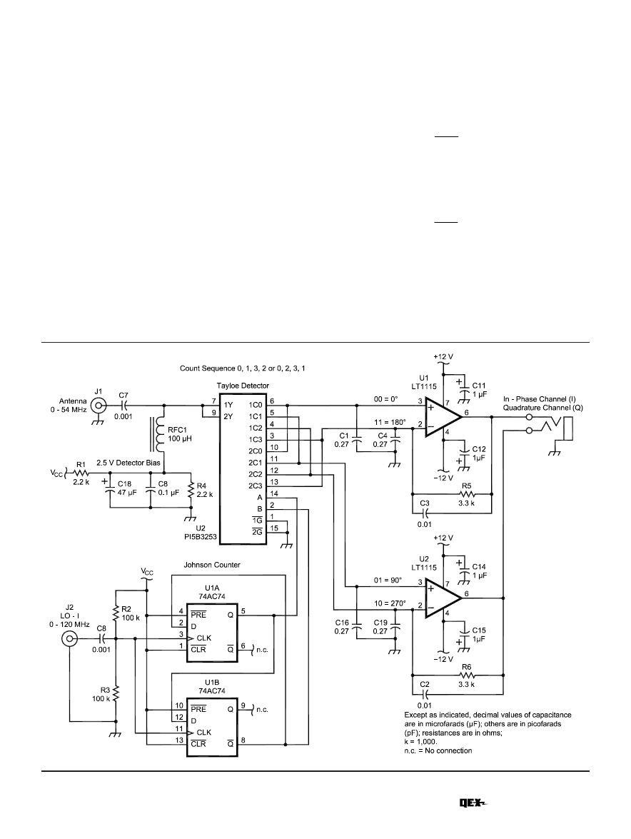
Fig 12 provides the schematic for a
simple, single-balanced Tayloe detec-
tor. It consists of a PI5V331, 1:4 FET
demultiplexer that switches the signal
to each of the four sampling capaci-
tors. The 74AC74 dual flip-flop is con-
nected as a divide-by-four Johnson
counter to provide the two-phase clock
to the demultiplexer chip. The outputs
of the sampling capacitors are differ-
entially summed through the two
LT1115 ultra-low-noise op amps to
form the I and Q outputs, respectively.
Note that the impedance of the
antenna forms the input resistance for
the op-amp gain as shown in Eq 7. This
impedance may vary significantly
with the actual antenna. I use instru-
mentation amplifiers in my final de-
sign to eliminate gain variance with
antenna impedance. More informa-
tion on the hardware design will be
provided in a future article.
Since the duty cycle of each switch
is 25%, the effective resistance in the
RC network is the antenna impedance
multiplied by four in the op-amp gain
formula, as shown in Eq 7:
ant
f
4R
R
G
=
(Eq 7)
For example, with a feedback resis-
tance, R
f
, of 3.3 k
Ω and antenna im-
pedance, R
ant
, of 50
Ω, the resulting
gain of the input stage is:
5
.
16
50
4
3300 =
×
=
G
Fig 12—Singly balanced Tayloe detector.
The Tayloe detector may also be
analyzed as a digital commutating fil-
ter.
,
as a very-high-Q tracking filter, where
determines the bandwidth and n
is the number of sampling capacitors,
20 Jul/Aug 2002
R
ant
is the antenna impedance and C
s
is the value of the individual sampling
capacitors. Eq 9 determines the Q
det
of the filter, where f
c
is the center fre-
quency and BW
det
is the bandwidth of
the filter.
s
ant
det
1
C
nR
BW
π
=
(Eq 8)
det
c
det
BW
f
Q
=
(Eq 9)
By example, if we assume the sam-
pling capacitor to be 0.27 µF and the
antenna impedance to be 50
Ω, then
BW and Q are computed as follows:
Hz
5895
)
10
7
.
2
)(
50
)(
4
)(
(
1
7
det
=
×
=
−
π
BW
2375
5895
10
001
.
14
6
det
=
×
=
Q
Since the PC SDR uses an offset
baseband IF, I have chosen to design
the detector’s bandwidth to be 40 kHz
to allow low-frequency noise elimina-
tion as discussed above.
The real payoff in the Tayloe detec-
tor is its performance. It has been
stated that the ideal commutating
mixer has a minimum conversion loss
(which equates to noise figure) of
3.9 dB.
mixers have a conversion loss of 6-7 dB
and noise figures 1 dB higher than the
loss. The Tayloe detector has less than
1 dB of conversion loss, remarkably.
How can this be? The reason is that it
is not really a mixer but a sampling
detector in the form of a quadrature
track and hold. This means that the
design adheres to discrete-time sam-
pling theory, which, while similar to
mixing, has its own unique character-
istics. Because a track and hold actu-
ally holds the signal value between
samples, the signal output never goes
to zero.
This is where aliasing can actually
be used to our benefit. Since each
switch and capacitor in the Tayloe
detector actually samples the RF sig-
nal once each cycle, it will respond to
alias frequencies as well as those
within the Nyquist frequency range.
In a traditional direct-conversion re-
ceiver, the local-oscillator frequency is
set to the carrier frequency so that the
difference frequency, or IF, is at 0 Hz
and the sum frequency is at two times
the carrier frequency per
normally remove the sum frequency
through low-pass filtering, resulting
in conversion loss and a corresponding
increase in noise figure. In the Tayloe
detector, the sum frequency resides at
the first alias frequency as shown in
Fig 13. Remember that an alias is a
real signal and will appear in the out-
put as if it were a baseband signal.
Therefore, the alias adds to the base-
band signal for a theoretically loss-
less detector. In real life, there is a
slight loss due to the resistance of the
switch and aperture loss due to imper-
fect switching times.
PC SDR Transceiver Hardware
The Tayloe detector therefore pro-
vides a low-cost, high-performance
method for both quadrature down-con-
version as well as up-conversion for
transmitting. For a complete system,
we would need to provide analog AGC
to prevent overload of the ADC inputs
and a means of digital frequency con-
trol. Fig 14 illustrates the hardware
architecture of the PC SDR receiver as
it currently exists. The challenge has
been to build a low-noise analog chain
that matches the dynamic range of the
Tayloe detector to the dynamic range
of the PC sound card. This will be cov-
ered in a future article.
I am currently prototyping a
complete PC SDR transceiver, the
SDR-1000, that will provide general-
coverage receive from 100 kHz to
54 MHz and will transmit on all ham
bands from 160 through 6 meters.
SDR Applications
At the time of this writing, the typi-
cal entry-level PC now runs at a clock
frequency greater than 1 GHz and
costs only a few hundred dollars. We
now have exceptional processing
power at our disposal to perform DSP
tasks that were once only dreams. The
transfer of knowledge from the aca-
Fig 13—Alias summing on Tayloe detector output: Since the Tayloe detector samples the
signal the sum frequency (
f c + f s) and its image (–f c – f s) are located at the first alias
frequency. The alias signals sum with the baseband signals to eliminate the mixing
product loss associated with traditional mixers. In a typical mixer, the sum frequency
energy is lost through filtering thereby increasing the noise figure of the device.
Fig 14—PC SDR receiver hardware architecture: After band-pass filtering the antenna is
fed directly to the Tayloe detector, which in turn provides
I and Q outputs at baseband. A
DDS and a divide-by-four Johnson counter drive the Tayloe detector demultiplexer. The
LT1115s offer ultra-low noise-differential summing and amplification prior to the wide-
dynamic-range analog AGC circuit formed by the SSM2164 and AD8307 log amplifier.
Jul/Aug 2002 21
demic to the practical is the primary
limit of the availability of this technol-
ogy to the Amateur Radio experi-
menter. This article series attempts to
demystify some of the fundamental
concepts to encourage experimenta-
tion within our community. The ARRL
recently formed a SDR Working Group
for supporting this effort, as well.
The SDR mimics the analog world in
digital data, which can be manipu-
lated much more precisely. Analog
radio has always been modeled math-
ematically and can therefore be pro-
cessed in a computer. This means that
virtually any modulation scheme may
be handled digitally with performance
levels difficult, or impossible, to attain
with analog circuits. Let’s consider
some of the amateur applications for
the SDR:
• Competition-grade HF transceivers
• High-performance IF for microwave
bands
• Multimode digital transceiver
• EME and weak-signal work
• Digital-voice modes
• Dream it and code it
For Further Reading
For more in-depth study of DSP
techniques, I highly recommend that
you purchase the following texts in
order of their listing:
Understanding Digital Signal Pro-
cessing by Richard G. Lyons (see Note
6). This is one of the best-written text-
books about DSP.
Digital Signal Processing Technol-
ogy by Doug Smith (see Note 4). This
new book explains DSP theory and
application from an Amateur Radio
perspective.
Digital Signal Processing in Com-
munications Systems by Marvin E.
Frerking (see Note 3). This book re-
lates DSP theory specifically to modu-
lation and demodulation techniques
for radio applications.
Acknowledgements
I would like to thank those who have
assisted me in my journey to under-
standing software radios. Dan Tayloe,
N7VE, has always been helpful and
responsive in answering questions
about the Tayloe detector. Doug Smith,
KF6DX, and Leif Åsbrink, SM5BSZ,
have been gracious to answer my ques-
tions about DSP and receiver design on
numerous occasions. Most of all, I want
to thank my Saturday-morning break-
fast review team: Mike Pendley,
WA5VTV; Ken Simmons, K5UHF; Rick
Kirchhof, KD5ABM; and Chuck
McLeavy, WB5BMH. These guys put
up with my questions every week and
have given me tremendous advice and
feedback all throughout the project. I
also want to thank my wonderful wife,
Virginia, who has been incredibly pa-
tient with all the hours I have put in on
this project.
Where Do We Go From Here?
Three future articles will describe
the construction and programming of
the PC SDR. The next article in the
series will detail the software interface
to the PC sound card. Integrating full-
duplex sound with DirectX was one of
the more challenging parts of the
project. The third article will describe
the Visual Basic code and the use of the
Intel Signal Processing Library for
implementing the key DSP algorithms
in radio communications. The final
article will describe the completed
transceiver hardware for the SDR-
1000.
11
D. H. van Graas, PA0DEN, “The Fourth
Method: Generating and Detecting SSB
Signals,”
QEX, Sep 1990, pp 7-11. This
circuit is very similar to a Tayloe detector,
but it has a lot of unnecessary compo-
nents.
12
M. Kossor, WA2EBY, “A Digital Commu-
tating Filter,”
QEX, May/Jun 1999, pp 3-8.
13
C. Ping, BA1HAM, “An Improved Switched
Capacitor Filter,”
QEX, Sep/Oct 2000, pp
41-45.
14
P. Anderson, KC1HR, “Letters to the Edi-
tor, A Digital Commutating Filter,”
QEX,
Jul/Aug 1999, pp 62.
15
D. Smith, KF6DX, “Notes on ‘Ideal’ Com-
mutating Mixers,”
QEX, Nov/Dec 1999,
pp 52-54.
16
P. Chadwick, G3RZP, “Letters to the Editor,
Notes on ‘Ideal’ Commutating Mixers” (Nov/
Dec 1999),
QEX, Mar/Apr 2000, pp 61-62.
Gerald became a ham in 1967 dur-
ing high school, first as a Novice and
then a General class as WA5RXV. He
completed his Advanced class license
and became KE5OH before finishing
high school and received his First
Class Radiotelephone license while
working in the television broadcast
industry during college. After 25 years
of inactivity, Gerald returned to the ac-
tive amateur ranks in 1997 when he
completed the requirements for Extra
class license and became AC5OG.
Gerald lives in Austin, Texas, and is
currently CEO of Sixth Market Inc, a
hedge fund that trades equities using
artificial-intelligence software. Gerald
previously founded and ran five tech-
nology companies spanning hardware,
software and electronic manufacturing.
Gerald holds a Bachelor of Science De-
gree in Electrical Engineering from
Mississippi Stage University.
Gerald is a member of the ARRL
SDR working Group and currently
enjoys homebrew software-radio devel-
opment, 6-meter DX and satellite op-
erations.
Notes
1
D. Smith, KF6DX, “Signals, Samples and
Stuff: A DSP Tutorial (Part 1),”
QEX, Mar/
Apr 1998, pp 3-11.
2
J. Bloom, KE3Z, “Negative Frequencies
and Complex Signals,”
QEX, Sep 1994,
pp 22-27.
3
M. E. Frerking,
Digital Signal Processing in
Communication Systems (New York: Van
Nostrand Reinhold, 1994, ISBN:
0442016166), pp 272-286.
4
D. Smith, KF6DX,
Digital Signal Processing
Technology (Newington, Connecticut:
ARRL, 2001), pp 5-1 through 5-38.
5
The Intel Signal Processing Library is avail-
able for download at
com/software/products/perflib/spl/
6
R. G. Lyons,
Understanding Digital Signal
Processing, (Reading, Massachusetts:
Addison-Wesley, 1997), pp 49-146.
7
D. Tayloe, N7VE, “Letters to the Editor,
Notes on‘Ideal’ Commutating Mixers (Nov/
Dec 1999),”
QEX, March/April 2001, p 61.
8
P. Rice, VK3BHR, “SSB by the Fourth
latrobe.edu.au/~rice/ssb/ssb.html
9
A. A. Abidi, “Direct-Conversion Radio
Transceivers for Digital Communications,”
IEEE Journal of Solid-State Circuits,
Vol 30, No 12, December 1995, pp 1399-
1410, Also on the Web at
edu/aagroup/PDF_files/dir-con.pdf
10
P. Y. Chan, A. Rofougaran, K.A. Ahmed,
and A. A. Abidi, “A Highly Linear 1-GHz
CMOS Downconversion Mixer.” Presented
at the European Solid State Circuits Con-
ference, Seville, Spain, Sep 22-24, 1993,
pp 210-213 of the conference proceed-
ings. Also on the Web at
Wyszukiwarka
Podobne podstrony:
The American Society for the Prevention of Cruelty
Efficient VLSI architectures for the biorthogonal wavelet transform by filter bank and lifting sc
eReport Wine For The Thanksgiving Meal
Herbs for the Urinary Tract
Mill's Utilitarianism Sacrifice the Innocent For the Commo
[Pargament & Mahoney] Sacred matters Sanctification as a vital topic for the psychology of religion
Derrida, Jacques «Hostipitality» Journal For The Theoretical Humanities
International Convention for the Safety of Life at Sea
Dig for the meaning?8
Rumpled cushions for the american dream
Magiczne przygody kubusia puchatka 23 SYMPATHY FOR THE DEVIL
Microsoft Word MIC1 Guidelines for the Generat
Broad; Arguments for the Existence of God(1)
ESL Seminars Preparation Guide For The Test of Spoken Engl
Hackmaster Quest for the Unknown Battlesheet Appendix
Kinesio taping compared to physical therapy modalities for the treatment of shoulder impingement syn
GB1008594A process for the production of amines tryptophan tryptamine
więcej podobnych podstron