VP2020L, BSS92
Vishay Siliconix
Document Number: 70210
S-04279—Rev. E, 16-Jun-01
www.vishay.com
11-1
P-Channel 200-V (D-S) MOSFETs
PRODUCT SUMMARY
Part Number
V
(BR)DSS
Min (V)
r
DS(on)
Max (
W
)
V
GS(th)
(V)
I
D
(A)
VP2020L
–200
20 @ V
GS
= –4.5 V
–0.8 to –2.5
–0.12
BSS92
–200
20 @ V
GS
= –10 V
–0.8 to –2.8
–0.15
FEATURES
BENEFITS
APPLICATIONS
D
High-Side Switching
D
Secondary Breakdown Free: –220 V
D
Low On-Resistance: 11.5
W
D
Low-Power/Voltage Driven
D
Excellent Thermal Stability
D
Ease in Driving Switches
D
Full-Voltage Operation
D
Low Offset Voltage
D
Easily Driven Without Buffer
D
No High-Temperature
“Run-Away”
D
Drivers: Relays, Solenoids, Lamps,
Hammers, Displays, Memories,
Transistors, etc.
D
Power Supply, Converters
D
Motor Control
D
Switches
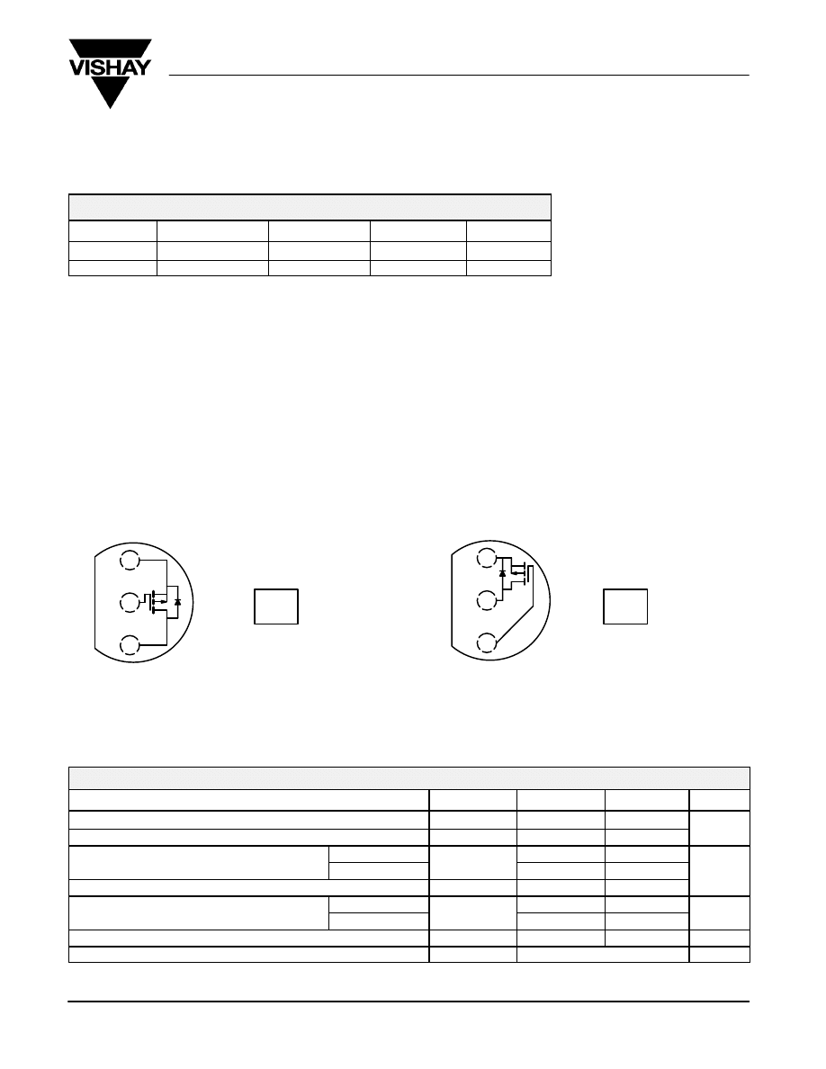
“S” VP
2020L
xxyy
TO-92-18CD
(TO-18 Lead Form)
Top View
S
G
D
1
2
3
1
TO-226AA
(TO-92)
Top View
S
D
G
2
3
BSS92
VP2020L
Device Marking
Front View
“S” = Siliconix Logo
xxyy = Date Code
“S” = Siliconix Logo
xxyy = Date Code
Device Marking
Front View
“S” BS
S92
xxyy
“S” = Siliconix Logo
xxyy = Date Code
Device Marking
Front View
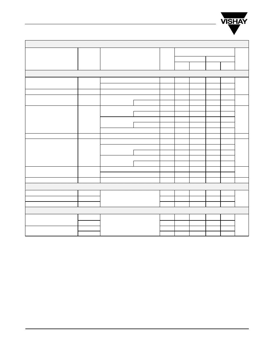
ABSOLUTE MAXIMUM RATINGS (T
A
= 25_C UNLESS OTHERWISE NOTED)
Parameter
Symbol
VP2020L
BSS92
Unit
Drain-Source Voltage
V
DS
–200
–200
Gate-Source Voltage
V
GS
"
20
"
20
V
_
T
A
= 25
_
C
–0.12
–0.15
Continuous Drain Current
(T
J
= 150
_
C)
T
A
= 100
_
C
I
D
–0.08
–0.09
A
Pulsed Drain Current
a
I
DM
–0.48
–0.6
T
A
= 25
_
C
0.8
1.0
Power Dissipation
T
A
= 100
_
C
P
D
0.32
0.4
W
Thermal Resistance, Junction-to-Ambient
R
thJA
156
125
_
C/W
Operating Junction and Storage Temperature Range
T
J
, T
stg
–55 to 150
_
C
Notes
a.
Pulse width limited by maximum junction temperature.
VP2020L, BSS92
Vishay Siliconix
www.vishay.com
11-2
Document Number: 70210
S-04279—Rev. E, 16-Jun-01
SPECIFICATIONS (T
A
= 25_C UNLESS OTHERWISE NOTED)
Limits
VP2020L
BSS92
Parameter
Symbol
Test Conditions
Typ
a
Min
Max
Min
Max
Unit
Static
Drain-Source
V
GS
= 0 V, I
D
= –10
m
A
–220
Drain-Source
Breakdown Voltage
V
(BR)DSS
V
GS
= 0 V, I
D
= –250
m
A
–220
–200
V
Gate-Threshold Voltage
V
GS(th)
V
DS
= V
GS
, I
D
= –1 mA
–1.9
–0.8
–2.5
–0.8
–2.8
V
DS
= 0 V, V
GS
=
"
20 V
"
10
"
100
Gate-Body Leakage
I
GSS
T
J
= 125
_
C
"
50
nA
V
DS
= 0.8 x V
(BR)DSS
, V
GS
= 0 V
–1
T
J
= 125
_
C
–100
Zero Gate Voltage
Drain Current
I
DSS
V
DS
= –200 V, V
GS
= 0 V
–60
m
A
Drain Current
DSS
T
J
= 125
_
C
–200
m
V
DS
= –60 V, V
GS
= 0 V
–0.2
On-State Drain Current
b
I
D(on)
V
DS
= –10 V, V
GS
= –4.5 V
–250
–100
mA
V
GS
= –10 V, I
D
= –0.1 A
11.5
20
V
GS
= –4.5 V, I
D
= –0.1 A
15
20
Drain-Source
On-Resistance
b
r
DS(on)
T
J
= 125
_
C
28
40
W
On-Resistance
b
DS(on)
V
GS
= –4.5 V, I
D
= –0.05 A
15
T
J
= 125
_
C
28
Forward
V
DS
= –10 V, I
D
= –0.1 A
170
100
Forward
Transconductance
b
g
fs
V
DS
= –25 V, I
D
= –0.1 A
170
60
mS
Diode Forward Voltage
V
SD
I
S
= –0.3 A, V
GS
= 0 V
–0.9
–1.2
V
Dynamic
Input Capacitance
C
iss
30
70
130
Output Capacitance
C
oss
V
DS
= –25 V, V
GS
= 0 V
f = 1 MHz
10
20
30
pF
Reverse Transfer Capacitance
C
rss
f = 1 MHz
3
10
15
Switching
c
t
d(on)
6
10
Turn-On Time
t
r
V
DD
= –25 V, R
L
= 250
W
^
8
15
I
D
^
–0.1 A, V
GEN
= –10 V
W
ns
t
d(off)
D
GEN
R
G
= 25
W
18
30
Turn-Off Time
t
f
R
G
= 25
W
17
25
Notes
a.
For DESIGN AID ONLY, not subject to production testing.
VPDQ20
b.
Pulse test: PW
v
300
m
s duty cycle
v
2%.
c.
Switching time is essentially independent of operating temperature.
VP2020L, BSS92
Vishay Siliconix
Document Number: 70210
S-04279—Rev. E, 16-Jun-01
www.vishay.com
11-3
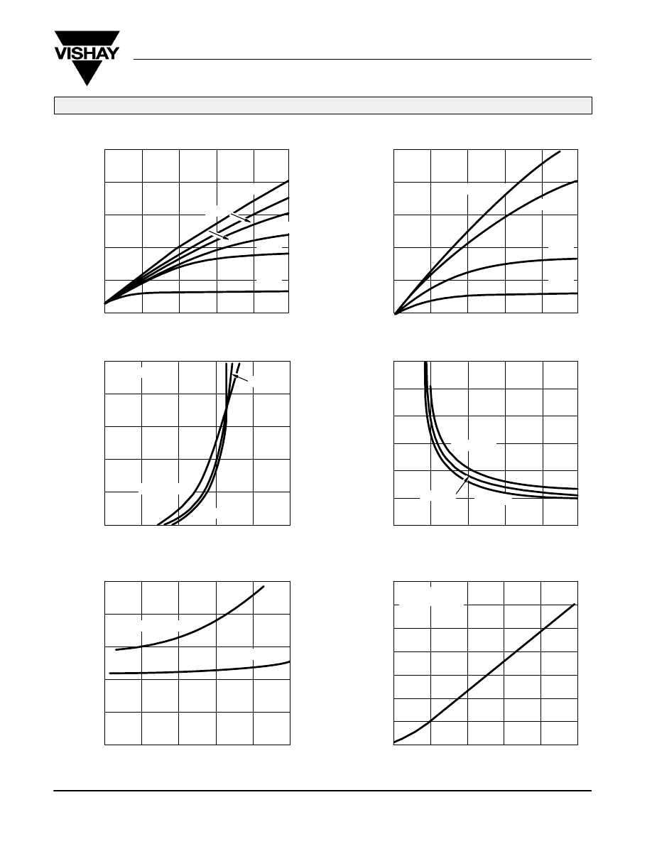
TYPICAL CHARACTERISTICS (T
A
= 25_C UNLESS OTHERWISE NOTED)
20
0
–4
–8
–12
–16
–20
18
16
14
12
10
8
–100
–80
–60
0
0
–1
–5
–40
–20
–2
–3
–4
–500
0
–1
–2
–3
–4
–5
–400
–300
–200
–100
0
Ohmic Region Characteristics
Output Characteristics for Low Gate Drive
On-Resistance
Normalized On-Resistance
vs. Junction Temperature
Transfer Characteristics
On-Resistance vs. Gate-to-Source Voltage
V
GS
– Gate-Source Voltage (V)
V
GS
– Gate-Source Voltage (V)
V
DS
– Drain-to-Source Voltage (V)
V
DS
– Drain-to-Source Voltage (V)
V
GS
= –10 V
–5 V
–6 V
–55
_
C
T
J
= 125
_
C
V
DS
= –15 V
–0.02 A
I
D
= –0.1 A
T
J
– Junction Temperature (
_
C)
–4.5 V
–4 V
–3 V
–100
0
–0.4
–0.8
–1.2
–1.6
–2.0
–80
–60
–40
–20
0
V
GS
= –4 V
–3.6 V
–3 V
–2 V
V
GS
– Gate-Source Voltage (V)
–0.05 A
25
20
15
0
0
–50
–250
10
5
–100
–150
–200
V
GS
= –4.5 V
–10 V
2.25
2.00
1.75
0.50
–50
–10
150
1.50
1.25
30
70
110
1.00
0.75
V
GS
= –4.5 V
I
D
= –0.1 A
25
_
C
I
D
–
Drain Current (mA)
I
D
–
Drain Current (mA)
I
D
–
Drain Current (mA)
r
DS
(on)
–
On-Resistance (
Ω )
r
DS
(on)
–
Drain-Source On-Resistance (
Ω )
r
DS
(on)
–
Drain-Source On-Resistance (
Ω )
(
Normalized)
VP2020L, BSS92
Vishay Siliconix
www.vishay.com
11-4
Document Number: 70210
S-04279—Rev. E, 16-Jun-01
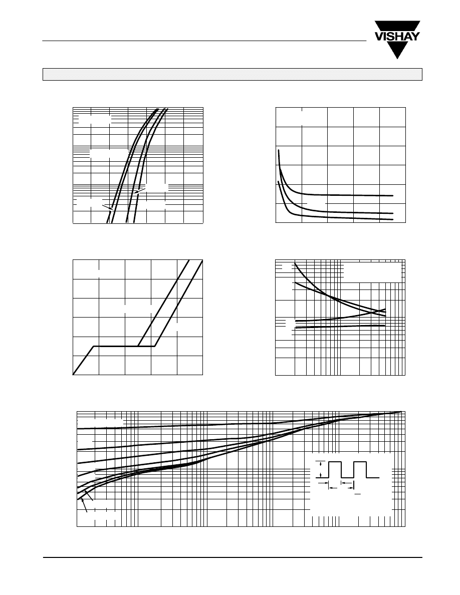
TYPICAL CHARACTERISTICS (T
A
= 25_C UNLESS OTHERWISE NOTED)
10 K
Duty Cycle = 0.5
0.2
0.1
0.05
0.02
Single Pulse
1
0.01
0.1
0.01
0.1
1.0
100
10
1 K
–10
–100
–1000
100
10
1
120
100
80
0
0
–10
–50
60
40
–20
–30
–40
20
Threshold Region
Capacitance
Normalized Effective Transient Thermal Impedance, Junction-to-Ambient (TO-226AA)
Gate Charge
Load Condition Effects on Switching
Normalized Ef
fective
T
ransient
Thermal Impedance
t
1
– Square Wave Pulse Duration (sec)
I
D
– Drain Current (A)
V
DS
– Drain-to-Source Voltage (V)
V
GS
– Gate-to-Source Voltage (V)
–55
_
C
Q
g
– Total Gate Charge (nC)
C
rss
C
oss
C
iss
V
DD
= –25 V
R
G
= 25
W
V
GS
= 0 to –10 V
t
d(on)
t
d(off)
t
r
t
f
T
J
= 150
_
C
1. Duty Cycle, D =
2. Per Unit Base = R
thJA
= 156
_
C/W
3. T
JM
– T
A
= P
DM
Z
thJA
(t)
t
1
t
2
t
1
Notes:
P
DM
t
2
–12
–10
–8
0
0
0.5
2.5
–6
–4
1.0
1.5
2.0
–2
I
D
= –0.1 A
V
DS
= –100 V
–160 V
–10.0
–1.0
–0.01
0
–3.5
–0.1
–1.0
–2.0
–3.0
V
DS
= –5 V
125
_
C
25
_
C
V
GS
= 0 V
f = 1 MHz
I
D
–
Drain Current (mA)
C
–
Capacitance (pF)
V
GS
–
Gate-to-Source V
oltage (V)
t
–
Switching T
ime (ns)
Wyszukiwarka
Podobne podstrony:
BYV27 50 BYV27 200 (Vishay)
BF970 Vishay elenota pl
BSS92
BF966S (Vishay)
BZX79 x2V4 x75 (Vishay)
SFH628A, SFH6286 (Vishay)
Si3430DV (Vishay)
XT26T (Vishay)
SUP40N25 60 (Vishay)
Vishay LTO 50
SFH615A, SFH6156 (Vishay)
BPW96 (Vishay)
XT49M (Vishay)
SFH617A [Vishay]
SUB65P06 20, SUP65P06 20 (Vishay)
MOC8050 (Vishay)
TCZT8020 (Vishay)
SFH618x (Vishay)
więcej podobnych podstron