Silan
Semiconductors
TX-2B/RX-2B
HANGZHOU SILAN MICROELECTRONICS JOINT-STOCK CO.,LTD
Rev: 1.0
2002.03.29
1
REMOTE CONTROLLER WITH FIVE
FUNCTIONS
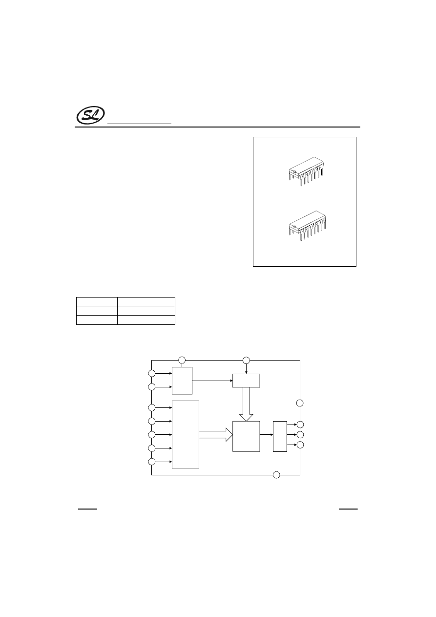
DESCRIPTION
The TX-2B/RX-2B is a pair of CMOS LSIs designed for remote
controlled car applications. The TX-2B/RX-2B has five control keys
for controlling the motions (i.e. forward, backward, rightward, leftward
and the turbo function ) of the remote controlled car.
FEATURES
* Wide operating voltage range (V
CC
=1.5~5.0V)
* Low stand-by current
* Auto-power-off function for TX-2B
* Few external components are needed
DIP-16
DIP-14
TX-2B
RX-2B
ORDERING INFORMATION
Part No.
Package
TX-2B
DIP-14-300-2.54
RX-2B
DIP-16-300-2.54
BLOCK DIAGRAM
Oscillator
Latch
Circuit
Encoding
Circuit
Timing
Generator
Logic
OSCI
OSCO
RIGHT
LEFT
TURBO
FORWARD
BACKWARD
PC
SO
SC
TEST B
GND
V
DD
FOSC
12
11
1
14
6
5
4
2
10
8
7
9
3
13
TRANSMITTER TX-2B Block Diagram
Silan
Semiconductors
TX-2B/RX-2B
HANGZHOU SILAN MICROELECTRONICS JOINT-STOCK CO.,LTD
Rev: 1.0
2002.03.29
2
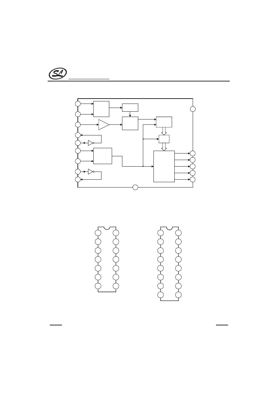
BLOCK DIAGRAM
LDB
RDB
SI
OSCO
OSCI
GND
4
5
3
9
8
2
RIGHT
LEFT
TURBO
BACKWARD
FORWARD
V
DD
7
11
10
12
6
13
Control
Logic
Decoding
Circuit
AMP
Timing
Generator
PLA
Computer
Latch
Circuit
VO2
VI2
16
1
VO1
VI1
14
15
Oscillator
RECEIVER RX-2B Block Diagram
PIN CONFIGURATION
TX
-2
B
RIGHT
TEST
GND
ACKWARD
FORWARD
TURBO
SC
PC
LEFT
FOSC
OSCI
OSCO
V
DD
SO
RX
-2
B
RIGHT
GND
BACKWARD
FORWARD
TURBO
LEFT
OSCI
OSCO
V
DD
VO2
SI
ROB
LDB
VI1
VO1
VI2
8
2
3
4
5
6
7
1
14
13
12
11
10
9
16
15
14
13
12
11
10
9
8
2
3
4
5
6
7
1
Silan
Semiconductors
TX-2B/RX-2B
HANGZHOU SILAN MICROELECTRONICS JOINT-STOCK CO.,LTD
Rev: 1.0
2002.03.29
3
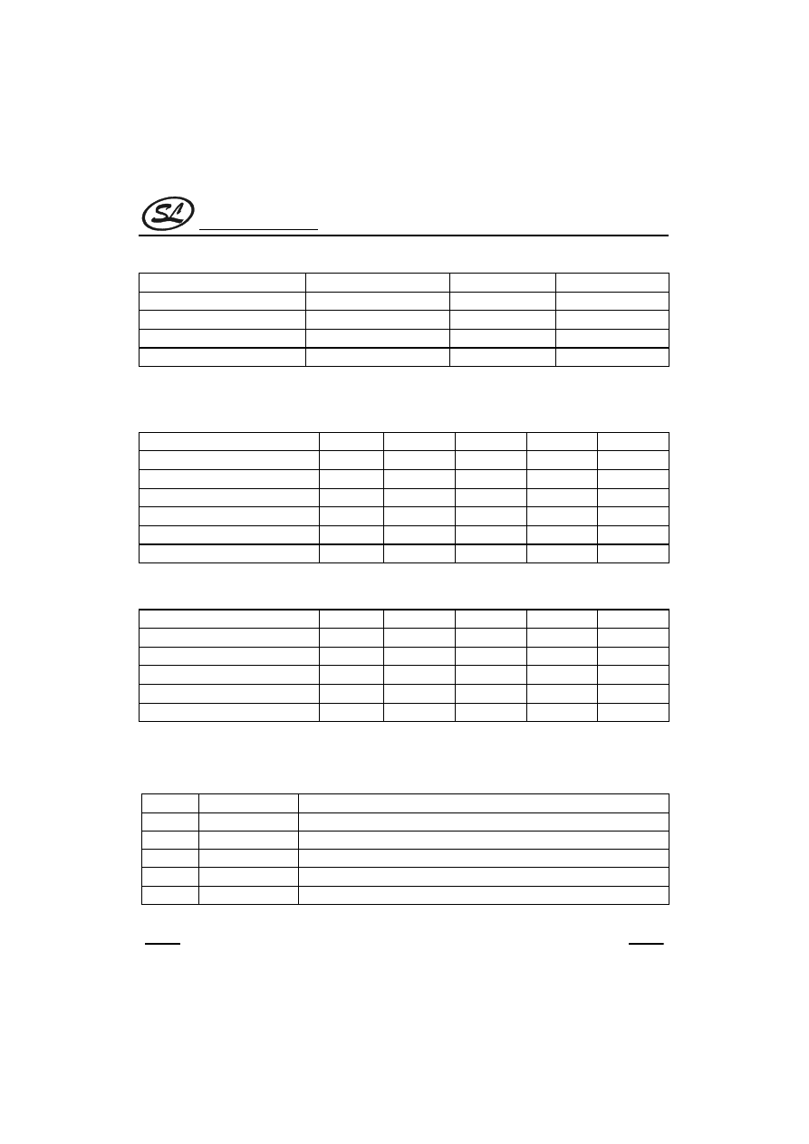
ABSOLUTE MAXIMUM RATINGS
Characteristic Symbol
Value
Unit
Supply Voltage
V
DD
0.3~5.0
V
Input / Output Voltage
V
IN
, V
OUT
GND-0.3~V
DD
+0.3
V
Operating Temperature
T
OPR
-10~65
°
C
Storage Temperature
T
stg
-25~125
°
C
ELECTRICAL CHARACTERISTICS
1. TX-2B
(
V
DD
=4.0V, F
osc
=128KHz, T
amb
=25
°
C, unless otherwise specified.)
Characteristic Symbol
Min
Typ
Max
Unit
Operating Voltage
V
DD
1.5
4.0
5.0
V
Operating Current
I
DD
--
--
2.0
mA
Stand-By Current
I
STB
--
--
10
µ
A
DC O/P Driving Current
I
drive
5
--
--
mA
AC O/P Driving Current
I
drive
5
--
--
mA
AC O/P Frequency
F
audio
0.5
--
1.0
kHz
2. RX-2B
(V
DD
=4.0V,F
osc
=128KHz, T
amb
=25
°
C, unless otherwise specified.)
characteristic Symbol
Min
Typ
Max
Unit
Operating Voltage
V
DD
1.5
4.0
5.0
V
Operating Current
I
DD
--
--
3.0
mA
O/P Driving Current
I
drive
1
--
--
mA
O/P Sinking Current
I
sink
1
--
--
mA
Effect Decoding Frequency Variation
F
tolerance
-20
--
20
%
PIN DESCRIPTION
1. TX-2B
Pin No.
Symbol
Description
1
RIGHT
The rightward function will be selected, if this pin is connected to GND
2
TEST
This pin is used for testing mode
3
GND
Negative power supply
4
BACKWARD
The backward function will be selected, if this pin is connected to GND
5
FORWARD
The forward function will be selected, if this pin is connected to GND
(To be continued)

Silan
Semiconductors
TX-2B/RX-2B
HANGZHOU SILAN MICROELECTRONICS JOINT-STOCK CO.,LTD
Rev: 1.0
2002.03.29
4
(Continued)
Pin No.
Symbol
Description
6
TURBO
The turbo function will be selected if this pin is connected to GND
7
SC
Output pin of the encoding signal with carrier frequency
8
SO
Output pin of the encoding signal without carrier frequency
9
V
DD
Positive power supply
10
PC
Power control output pin
11
OSCO
Oscillator output pin
12
OSCI
Oscillator input pin
13
FOSC
This pin is used for testing mode
14
LEFT
The leftward function will be selected, if this pin is connected to GND
2. RX-2B
Pin No.
Symbol
Description
1
VO2
Inverter 2 output pin for power amplify
2
GND
Negative power supply
3
SI
Input pin of the encoding signal
4
OSCI
Oscillator input pin
5
OSCO
Oscillator output pin
6
RIGHT
Rightward output pin
7
LEFT
Leftward output pin
8
ROB
Rightward function disable, if this pin is connected to GND
9
LDB
Leftward function disable, if this pin is connected to GND
10
BACKWARD
Backward output pin
11
FORWARD
Forward output pin
12
TURBO
TURBO output pin
13
V
DD
Positive power supply
14
VI1
Inverter 1 input pin for power amplify
15
VO1
Inverter 1 output pin for power amplify
16
VI2
Inverter 2 input pin for power amplify
Silan
Semiconductors
TX-2B/RX-2B
HANGZHOU SILAN MICROELECTRONICS JOINT-STOCK CO.,LTD
Rev: 1.0
2002.03.29
5
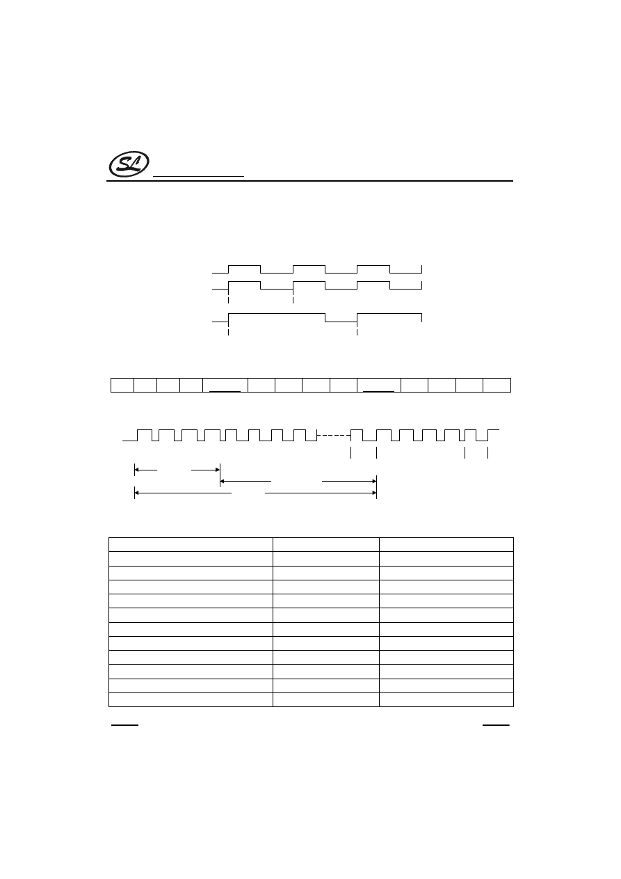
CODE FORMAT
1. ENCODE RULE
(A).Bit Format (W1 is used for function codes,W2 for start codes)
1KHz
W1
1KHz 50% Duty cycle
W2
500Hz 75% Duty cycle
(B).Date Format
W2
W2
W2
W2
(n) X W1
W2
W2
W2
W2
(n) X W1
W2
W2
W2
W2
W2
W2
W2
W2
1
2
3
4
1
2
3
4
W1
W1
W1
W1
W1
W1
W2
W2
W2
n-th
start code
function code
1 word
W2
n x W1
Number Of Function Code (N) W1
Function Key
Decode Result
4
End Code
10
Forward
Forward
16
Forward & Turbo
Forward
22
Turbo
Turbo
28
Turbo & Forward & Left
Forward & Left
34
Turbo & Forward & Right
Forward & Right
40
Backward
Backward
46
Backward & Right
Backward & Right
52
Backward & Left
Backward & Left
58
Left
Left
64
Right
Right
Silan
Semiconductors
TX-2B/RX-2B
HANGZHOU SILAN MICROELECTRONICS JOINT-STOCK CO.,LTD
Rev: 1.0
2002.03.29
6
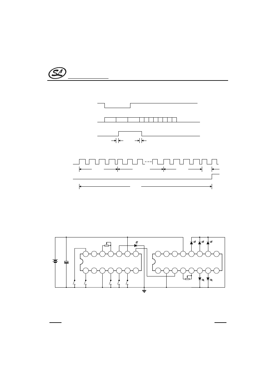
2. ENCODE/DECODE TIMING
Any function key
Encode output
Decode output
1st word
2nd word
3rd word
1
2
3
4
5
6
7
8
9ms
9ms
end code
T
(n) W1
8ms
1ms
SI
Decode output
T=17ms+(nW1)x1ms
8ms
TESTING CIRCUIT
(The oscillator frequency of TX-2B, RX-2B is 128KHz, the oscillator resistor is 160K
Ω
and 250K
Ω
respectively)
TX-2B
RX-2B
100
F
le
ft
ri
ght
forwar
d
bac
kw
ard
turbo
le
ft
ri
ght
back
w
ar
d
forward
turbo
f
osc
=128kHz
f
osc
=128kHz
V
CC=3
V
14
13
12
11
8
10
9
1
2
3
4
7
5
6
1
2
3
4
7
5
6
8
14
13
12
11
10
9
15
16
Silan
Semiconductors
TX-2B/RX-2B
HANGZHOU SILAN MICROELECTRONICS JOINT-STOCK CO.,LTD
Rev: 1.0
2002.03.29
7
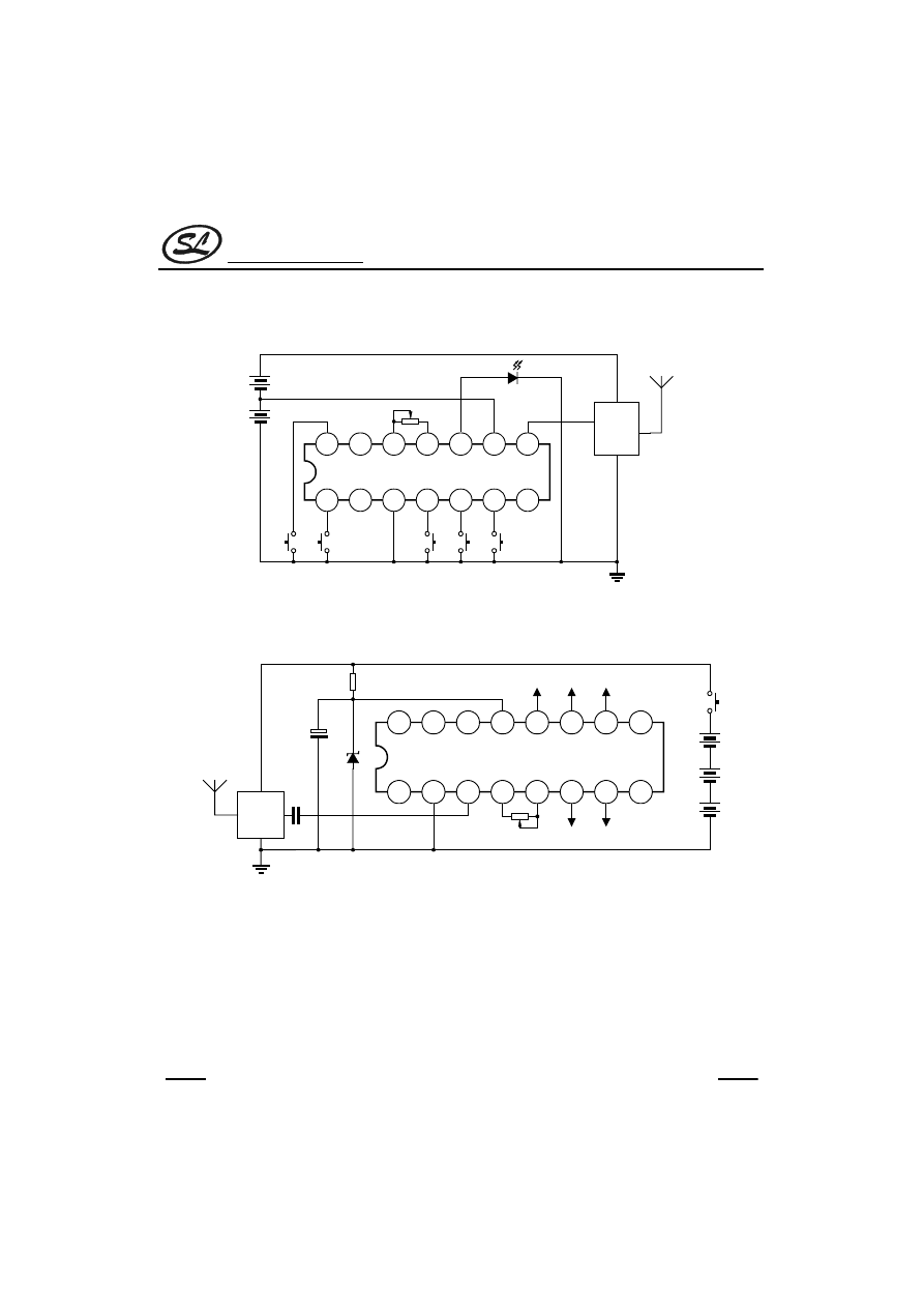
TYPICAL APPLICATION CIRCUIT
TRANSMITTER
SI
R
osc
=500k
¡
R.F.
CIRCUIT
V
CC
TX-2B
left
ri
ght
backwa
rd
forw
ar
d
turbo
1
2
3
4
5
6
7
14
13
12
11
10
9
8
RECEIVER
RX-2B
power
switch
100
F
4.3V
R.F.
CIRCUIT
GND
V
CC
500k
¡
1
2
3
4
5
6
7
8
15
14
13
12
11
10
9
16
Silan
Semiconductors
TX-2B/RX-2B
HANGZHOU SILAN MICROELECTRONICS JOINT-STOCK CO.,LTD
Rev: 1.0
2002.03.29
8
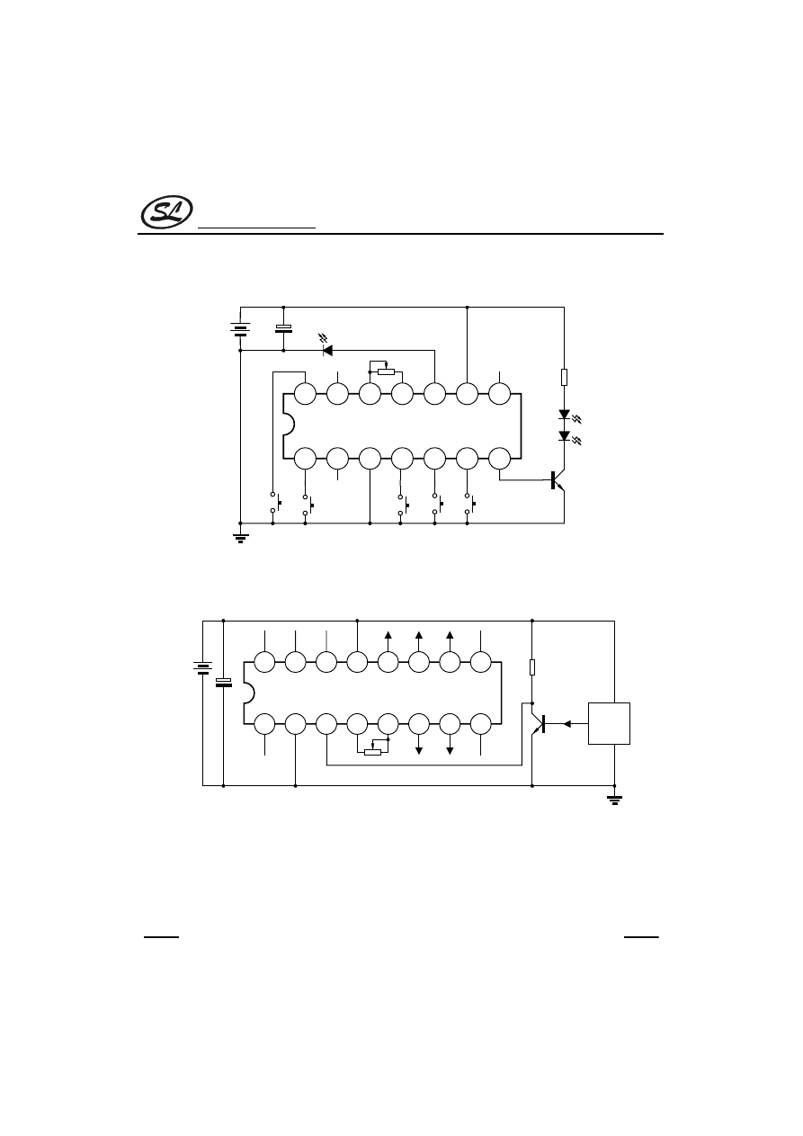
INFRARED APPLICATION CIRCUIT
TRANSMITTER
TX-2B
f
osc
=114kHz
C8050
P
hot
o
D
iode
1~
4.
7
¡
100
F
DC:
3V
Lef
t
Right
F
ront
war
d
Ba
ck
w
ar
d
Tu
rb
o
14
13
12
11
10
9
8
2
3
4
5
6
7
1
RECEIVER
RX-2B
f
osc
=114KHz
1815
100K
¡
DC:5V
10
0
F
V
DD
IR
Receiver
GND
OUT
16
15
14
13
12
11
9
10
1
2
3
4
5
6
8
7
Silan
Semiconductors
TX-2B/RX-2B
HANGZHOU SILAN MICROELECTRONICS JOINT-STOCK CO.,LTD
Rev: 1.0
2002.03.29
9
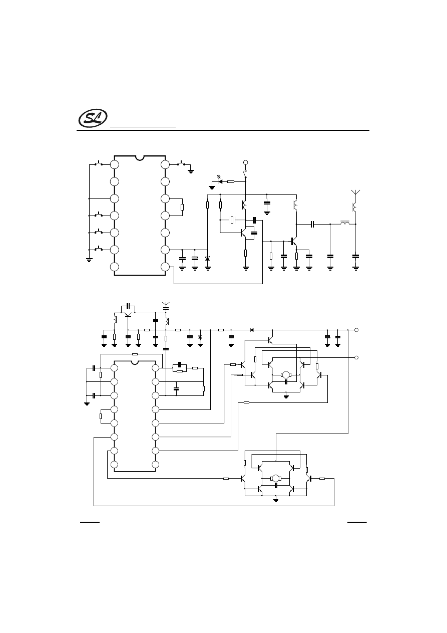
RECOMMENDED APPLICATION CIRCUIT
TX-2B
2
1
3
5
4
6
14
12
13
11
7
8
10
9
Ros
c
=
16
0K
39
0
¡
22
0k
¡
1.5k
¡
LED
L
R
B
F
TURBO
10
0
¡
33
K
¡
10
0
¡
68
P
20
3P
151P
2
03P
15
1P
10
3P
L3
L1
2.2
H
47P
68
P
2
03P
47
F
3.
0V
V
DD
=9V
L2
2.2
H
L4
6.8
H
7T 0.3mm (
)
x 5mm(Core)
Q1
Q2
C945
C945
XTAL
27MHz
RX-2B
M
M
Ro
s
c
=
2
5
0
K
3.
3
k
¡
82
0
¡
R2
3.3k
¡
3.
3k
¡
390
¡
330
¡
3.9MO
3.
9M
¡
1N4148
1k
¡
1k
¡
1kO
1k
¡
1k
¡
R4
R3
R2
R1
100
F
/16V
470
F
/16V
220
F
/16V
4.
7
F
C
1
10
2P
C2 47P
C3
1
8
P
C
4
20
3P
180k
¡
4P
203P
222P
50
1P
103P
473P
473P
10
4P
L1
1.
1
F
L2
10
4P
3.0V
Q1
Q3
Q2
Q5
Q4
Q6
C945
C945
C945
Q7
Q8
Q9
Q10
C945
C945
R1,R2,R3,R4=80~150
¡
,are
changeable with the V
DD1
and
V
DD2.
Q1: C9018,C1815,C380,C382
Q2,Q3,Q4: 5610,C8550,B772
Q5,Q6: C8050,5609,D882
Q7,Q8: B564,C8550,B772
Q9,Q10: D471,C8050,D882
V
DD1
=12V,R=330
¡
V
DD1
=9V,R=220
¡
V
DD1
V
DD2
7T 0.3mm (
)
x 5mm(Core)
2
1
3
5
4
6
15
16
14
12
13
11
7
8
10
9
left
right
turbo
forward
backward
Silan
Semiconductors
TX-2B/RX-2B
HANGZHOU SILAN MICROELECTRONICS JOINT-STOCK CO.,LTD
Rev: 1.0
2002.03.29
10
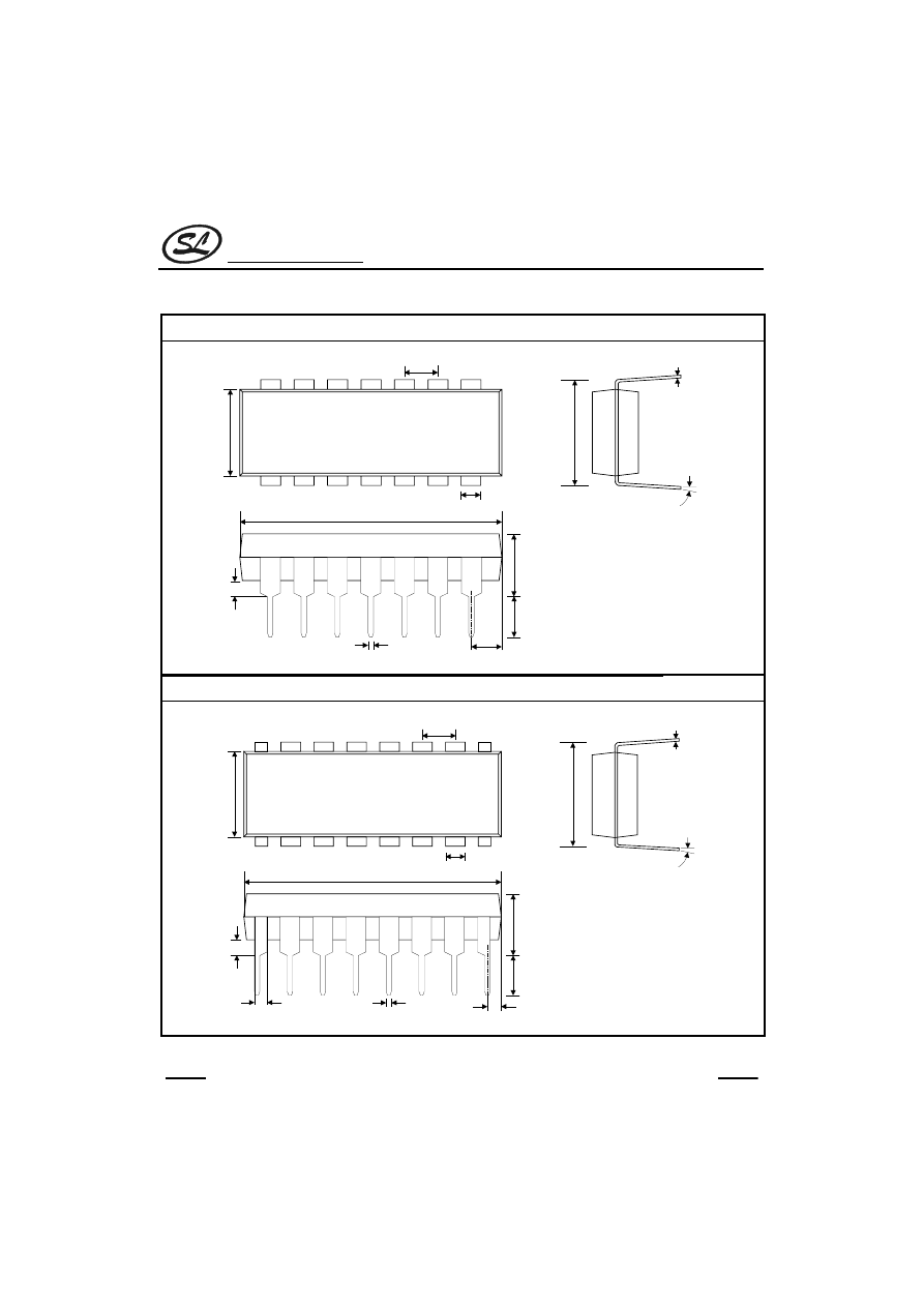
PACKAGE OUTLINE
DIP-14-300-2.54
UNIT: mm
6.3
5
B
0.2
5
2.54
4.3
6
M
A
X
3.0
0
M
IN
7.
6
2
15 degree
0.46
B
0.08
19.55
B
0.3
1.52
0.
5MI
N
0.2
5
B
0.0
5
2.40MAX
DIP-16-300-2.54
UNIT: mm
6.35
B
0.
2
5
2.54
4.3
6
MA
X
3
.00MIN
7.62
15 degree
0.46
B
0.08
19.55
B
0.3
1.52
0.25
B
0.
0
5
0.5M
IN
1.27MAX
0.99
B
0.3
Wyszukiwarka
Podobne podstrony:
Design the Remote Control System With the Time Delay Estimator and the Adaptive Smith Predictor ge2
moto suzuki motorbike scanner with bluetooth function list
Panasonic Eur 516Xx Series Universal Remote Control
315mhz 433mhz remote control code scanner coppier
Creating Custom Net Controls With C Sharp
how to use fgtech with bdm function
4 kanaly Remote Control UHF 433 Nieznany (2)
Panasonic Eur 517Xx Series Universal Remote Control
moto suzuki motorbike scanner with bluetooth function list
SSP 406 DCC Adaptive Chassis Control Design and Function
Panasonic Eur 516Xx Series Universal Remote Control
Samsung Universal Remote Control Programming
Philips service mode remote control codes (word95)
Panasonic Eur 517Xx Series Universal Remote Control
Baumann Destabilization of velocity feedback controllers with stroke limited inertial actuators
15 E65 Remote Control Service
Repairing Remote Controls Notes
więcej podobnych podstron