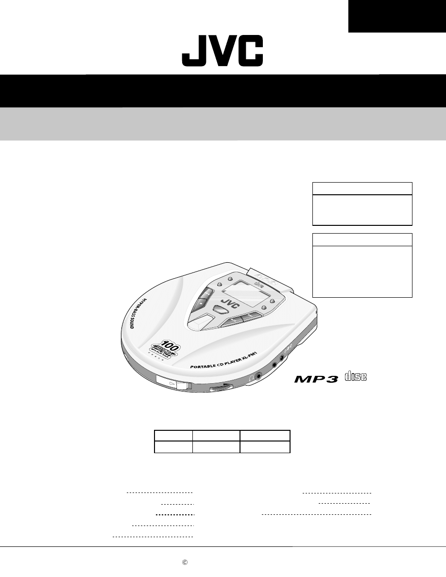
SERVICE MANUAL
PORTABLE CD PLAYER
No.21018
Jul. 2001
COPYRIGHT 2001 VICTOR COMPANY OF JAPAN, LTD.
COMPACT
DIGITAL AUDIO
CO
MPA
CT
DIG
ITA
L A
UD
IO
REPEA
T/
RAN
DOM
HBS
+10
GR
OUP
ESP
RES
UME
Volume
D
C
IN
4
.5
V
OPE
N
Lin
e O
ut
Contents
Safety Precautions
Important for laser products
Preventing static electricity
Disassembly method
Troubleshooting
Explanation of MP3
Description of major ICs
Parts list
1-2
1-3
1-4
1-5
1-7
1-8
1-9
1-13 ~18
XL-PM11/XL-PM1
XL-PM11/XL-PM1
Area Suffix
XL-PM1
J ------------------------ U.S.A.
C --------------------- Canada
B -------------------------- U.K.
E ------ Continental Europe
XL-PM11
C --------------------- Canada
Area Suffix
XL-PM11
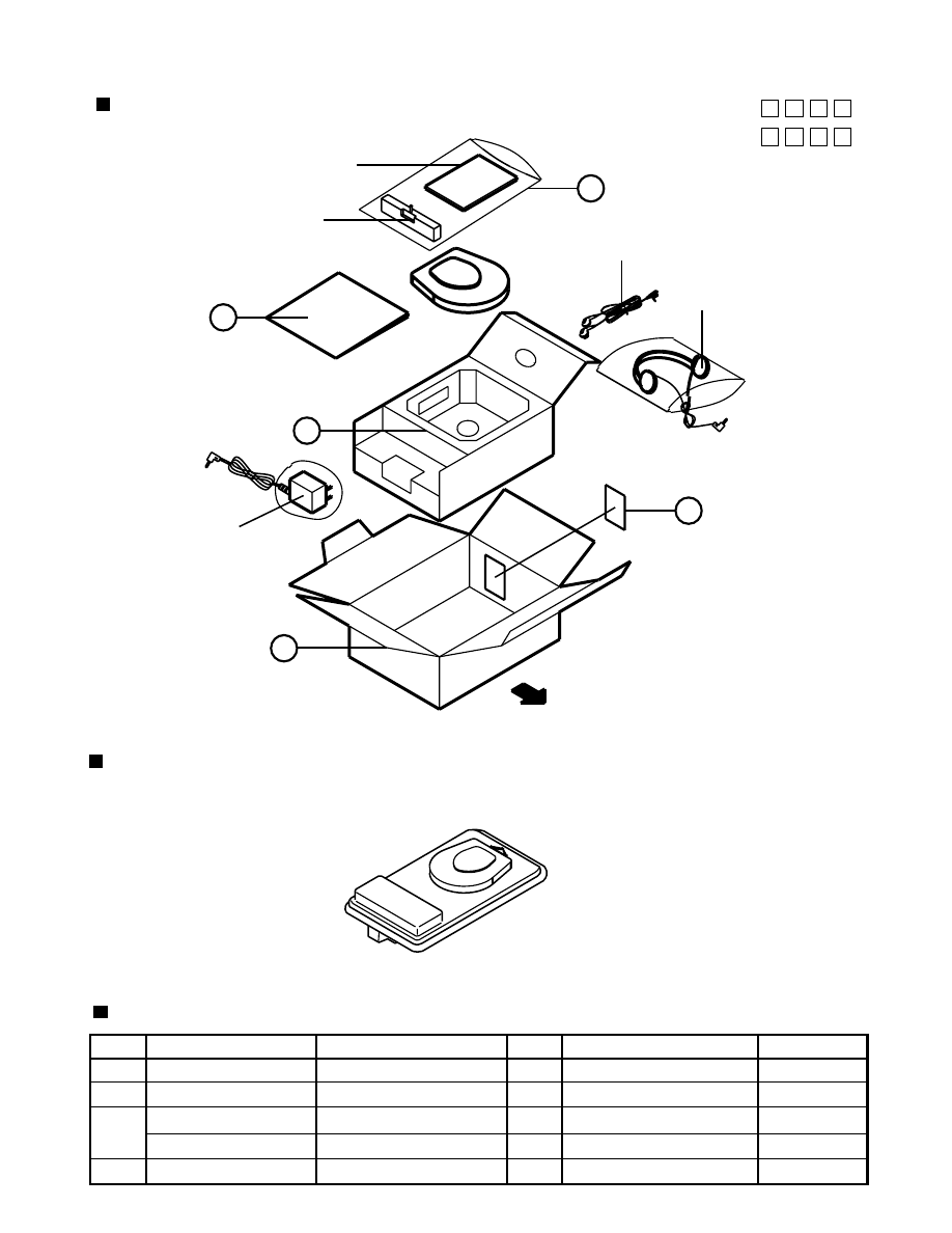
Gift box
XL-PM1
Blister pack
PACKING
Model XL-PM11 is an exclusive use for Canada. As for
the difference between XL-PM11 and XL-PM1, the
packing specification is different.
XL-PM11/XM-PM1
1-2
1. This design of this product contains special hardware and many circuits and components specially for safety
purposes. For continued protection, no changes should be made to the original design unless authorized in
writing by the manufacturer. Replacement parts must be identical to those used in the original circuits. Services
should be performed by qualified personnel only.
2. Alterations of the design or circuitry of the product should not be made. Any design alterations of the product
should not be made. Any design alterations or additions will void the manufacturer`s warranty and will further
relieve the manufacture of responsibility for personal injury or property damage resulting therefrom.
3. Many electrical and mechanical parts in the products have special safety-related characteristics. These
characteristics are often not evident from visual inspection nor can the protection afforded by them necessarily
be obtained by using replacement components rated for higher voltage, wattage, etc. Replacement parts which
have these special safety characteristics are identified in the Parts List of Service Manual. Electrical
components having such features are identified by shading on the schematics and by ( ) on the Parts List in
the Service Manual. The use of a substitute replacement which does not have the same safety characteristics
as the recommended replacement parts shown in the Parts List of Service Manual may create shock, fire, or
other hazards.
4. The leads in the products are routed and dressed with ties, clamps, tubings, barriers and the like to be
separated from live parts, high temperature parts, moving parts and/or sharp edges for the prevention of
electric shock and fire hazard. When service is required, the original lead routing and dress should be
observed, and it should be confirmed that they have been returned to normal, after re-assembling.
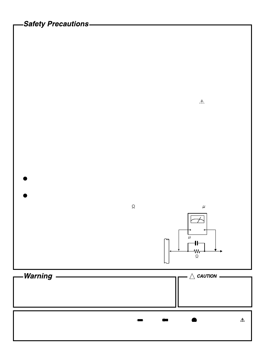
5. Leakage currnet check (Electrical shock hazard testing)
After re-assembling the product, always perform an isolation check on the exposed metal parts of the product
(antenna terminals, knobs, metal cabinet, screw heads, headphone jack, control shafts, etc.) to be sure the
product is safe to operate without danger of electrical shock.
Do not use a line isolation transformer during this check.
Plug the AC line cord directly into the AC outlet. Using a "Leakage Current Tester", measure the leakage
current from each exposed metal parts of the cabinet, particularly any exposed metal part having a return
path to the chassis, to a known good earth ground. Any leakage current must not exceed 0.5mA AC (r.m.s.).
Alternate check method
Plug the AC line cord directly into the AC outlet. Use an AC voltmeter having, 1,000 ohms per volt or more
sensitivity in the following manner. Connect a 1,500 10W resistor paralleled by a 0.15 F AC-type capacitor
between an exposed metal part and a known good earth ground.
Measure the AC voltage across the resistor with the AC
voltmeter.
Move the resistor connection to each exposed metal part,
particularly any exposed metal part having a return path to
the chassis, and meausre the AC voltage across the resistor.
Now, reverse the plug in the AC outlet and repeat each
measurement. Voltage measured any must not exceed 0.75 V
AC (r.m.s.). This corresponds to 0.5 mA AC (r.m.s.).
1. This equipment has been designed and manufactured to meet international safety standards.
2. It is the legal responsibility of the repairer to ensure that these safety standards are maintained.
3. Repairs must be made in accordance with the relevant safety standards.
4. It is essential that safety critical components are replaced by approved parts.
5. If mains voltage selector is provided, check setting for local voltage.
Good earth ground
Place this
probe on
each exposed
metal part.
AC VOLTMETER
(Having 1000
ohms/volts,
or more sensitivity)
1500 10W
0.15 F AC TYPE
!
Burrs formed during molding may
be left over on some parts of the
chassis. Therefore, pay attention to
such burrs in the case of
preforming repair of this system.
In regard with component parts appearing on the silk-screen printed side (parts side) of the PWB diagrams, the
parts that are printed over with black such as the resistor ( ), diode ( ) and ICP ( ) or identified by the " "
mark nearby are critical for safety.
When replacing them, be sure to use the parts of the same type and rating as specified by the manufacturer.
(Except the J and C version)
XL-PM11/XM-PM1
1-3
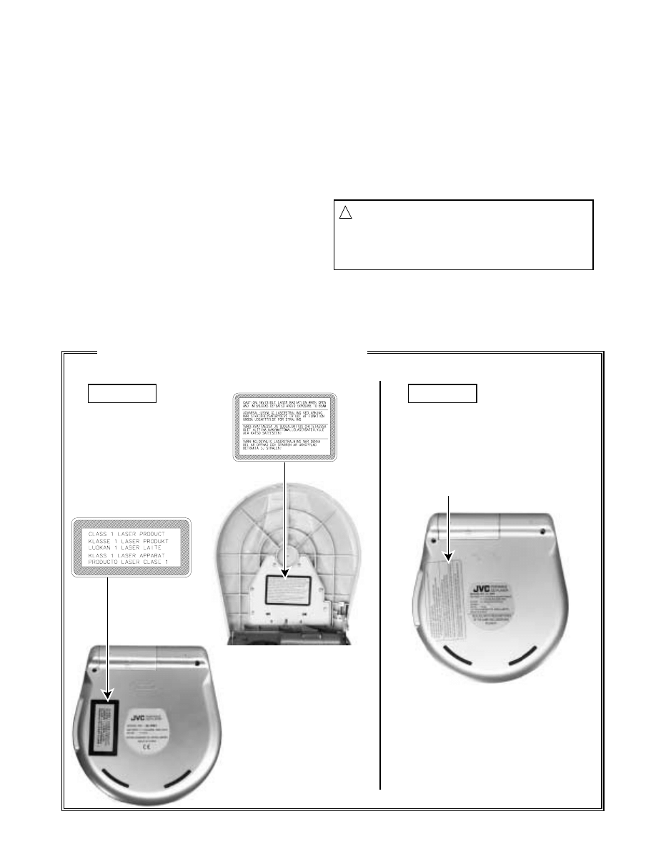
Important for laser products
1.CLASS 1 LASER PRODUCT
2.DANGER : Invisible laser radiation when open and inter
lock failed or defeated. Avoid direct exposure to beam.
3.CAUTION : There are no serviceable parts inside the
Laser Unit. Do not disassemble the Laser Unit. Replace
the complete Laser Unit if it malfunctions.
4.CAUTION : The compact disc player uses invisible
laserradiation and is equipped with safety switches which
prevent emission of radiation when the drawer is open and
the safety interlocks have failed or are de
feated. It is dangerous to defeat the safety switches.
5.CAUTION : If safety switches malfunction, the laser is able
to function.
6.CAUTION : Use of controls, adjustments or performance of
procedures other than those specified herein may result in
hazardous radiation exposure.
!
CAUTION
Please use enough caution not to
see the beam directly or touch it
in case of an adjustment or operation
check.
WARNING LABEL
DHHS LABEL
CLASS 1
LASER PRODUCT
(Cabinet -bottom)
(Cabinet -door/ inside)
Reproduction and position of labels
B, E version
J, C version
XL-PM11/XM-PM1
1-4
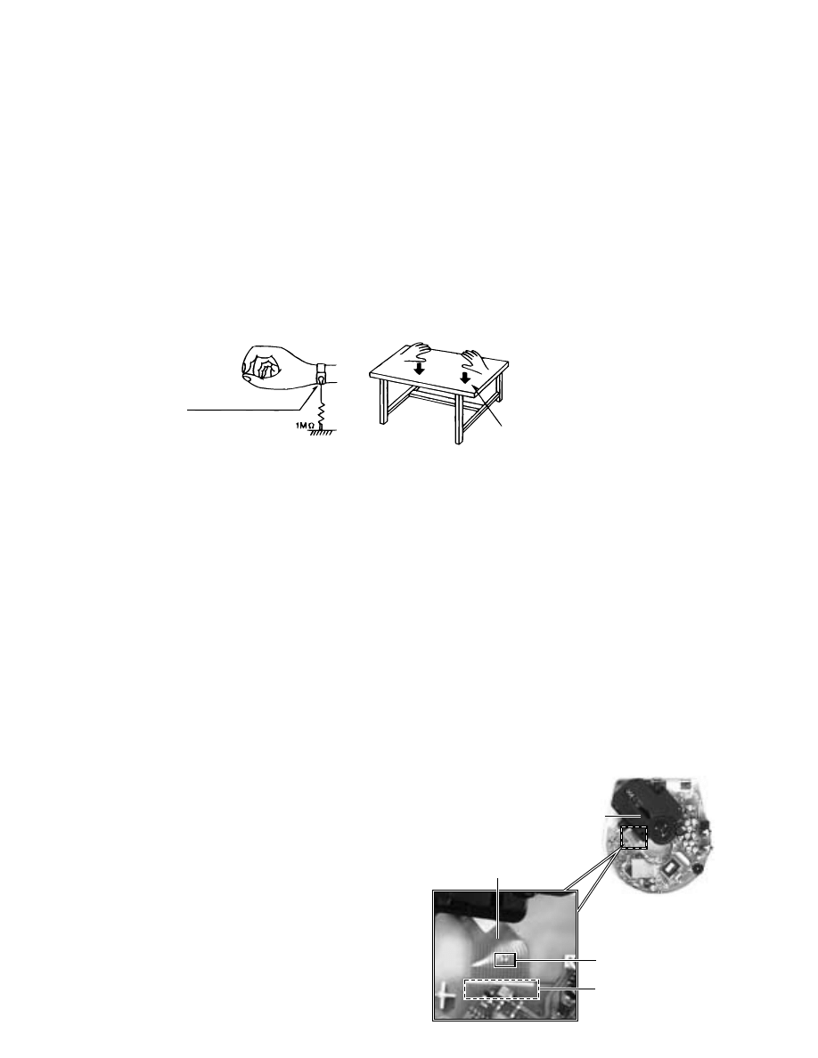
Preventing static electricity
1. Grounding to prevent damage by static electricity
Electrostatic discharge (ESD), which occurs when static electricity stored in the body, fabric, etc. is discharged,
can destroy the laser diode in the traverse unit (optical pickup). Take care to prevent this when performing repairs.
2. About the earth processing for the destruction prevention by static electricity
In the equipment which uses optical pick-up (laser diode), optical pick-up is destroyed by the static electricity of
the work environment.
Be careful to use proper grounding in the area where repairs are being performed.
2-1 Ground the workbench
Ground the workbench by laying conductive material (such as a conductive sheet) or an iron plate over
it before placing the traverse unit (optical pickup) on it.
2-2 Ground yourself
Use an anti-static wrist strap to release any static electricity built up in your body.
3. Handling the optical pickup
1. In order to maintain quality during transport and before installation, both sides of the laser diode on the
replacement optical pickup are shorted. After replacement, return the shorted parts to their original condition.
(Refer to the text.)
2. Do not use a tester to check the condition of the laser diode in the optical pickup. The tester's internal power
source can easily destroy the laser diode.
4. Handling the traverse unit (optical pickup)
1. Do not subject the traverse unit (optical pickup) to strong shocks, as it is a sensitive, complex unit.
2. Cut off the shorted part of the flexible cable using nippers, etc. after replacing the optical pickup. For specific
details, refer to the replacement procedure in the text. Remove the anti-static pin when replacing the traverse
unit. Be careful not to take too long a time when attaching it to the connector.
3. Handle the flexible cable carefully as it may break when subjected to strong force.
4. It is not possible to adjust the semi-fixed resistor that adjusts the laser power. Do not turn it.
Conductive material
(conductive sheet) or iron plate
(caption)
Anti-static wrist strap
Flexible board
CD mechanism
assembly
short-circuit land
CON1
on the main board
1.
2.
3.
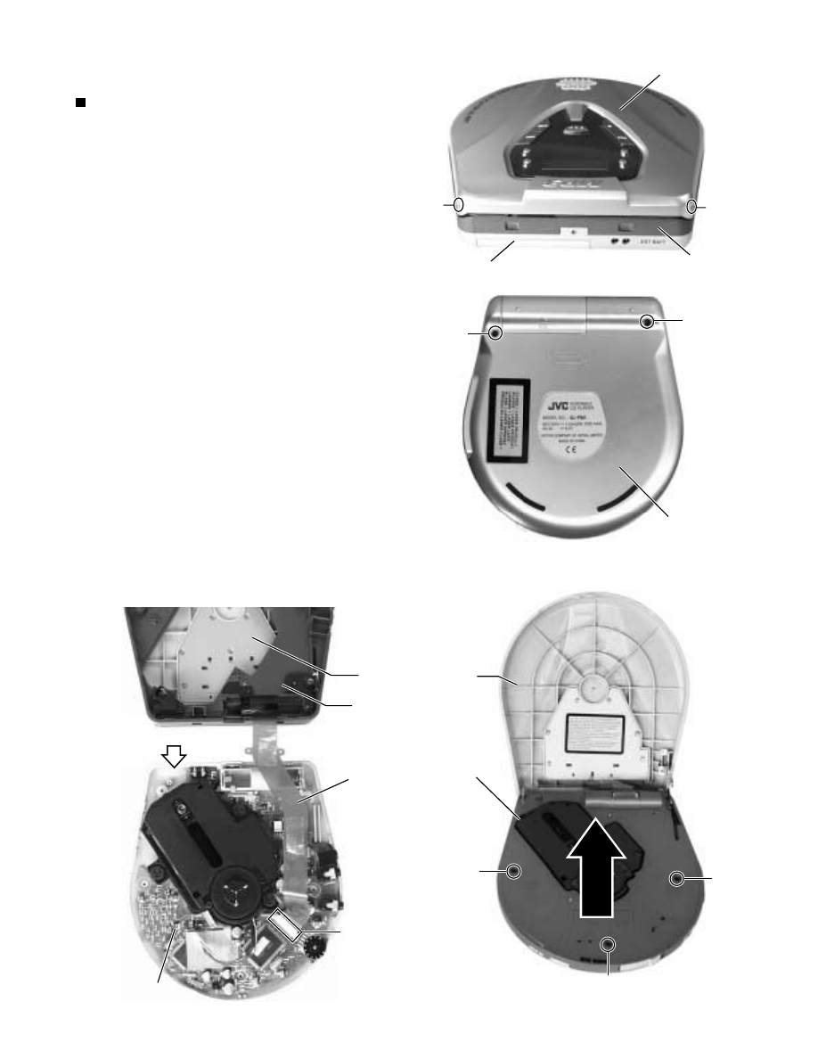
Remove the door & middle cabinet.
Solder the short-circuit land on the flexible board, before the
flexible board is removed from connector CON1 on the main
board.
(When the flexible board is removed without putting up solder,
the CD mechanism assembly might destroy.)
Please unsolder the short-circuit land after connecting the
flexible board with the CON1 on the main board, when you
install CD mechanism assembly in the substrate.
Attention when CD mechanism assembly is decomposed
*Please refer to "Disassembly method" in the text for pick-up and how to
detach the CD mechanism assembly.
XL-PM11/XM-PM1
1-5
Remove the two screws A attaching the cabinet -
door on the back of the body.
Remove the two screws B on the cabinet -bottom.
Remove the three screws C attaching the cabinet -
middle and remove the cabinet -middle from the
cabinet -bottom.
ONE POINT:
Disconnect the flexible board from connector
FRW000 on the main board, and remove the cabinet
-door with cabinet -middle.
1.
2.
3.
4.
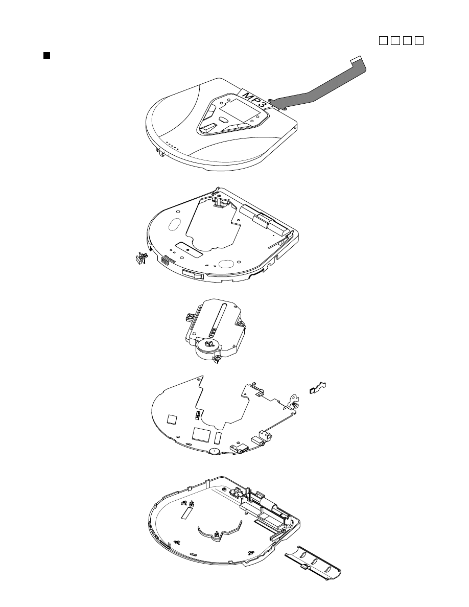
Disassembly method
Removing the cabinet -door & cabinet
-middle (See Fig.1 to 4)
Flexible board is bonded with couple-
face tapes internally in the cabinet -
middle.
Fig.1
Fig.2
(The photograph is one of
the B and E version. )
Fig.3
(The photograph is one of
the B and E version. )
A
A
B
B
C
C
C
Cabinet -door
Cabinet -door (inside)
Fig.4
FRW000
Main board
Cabinet -middle
Cabinet -middle
Cabinet -middle (inside)
Cabinet -bottom
Cabinet -bottom
Cabinet -bottom (inside)
Flexible board
XL-PM11/XM-PM1
1-6
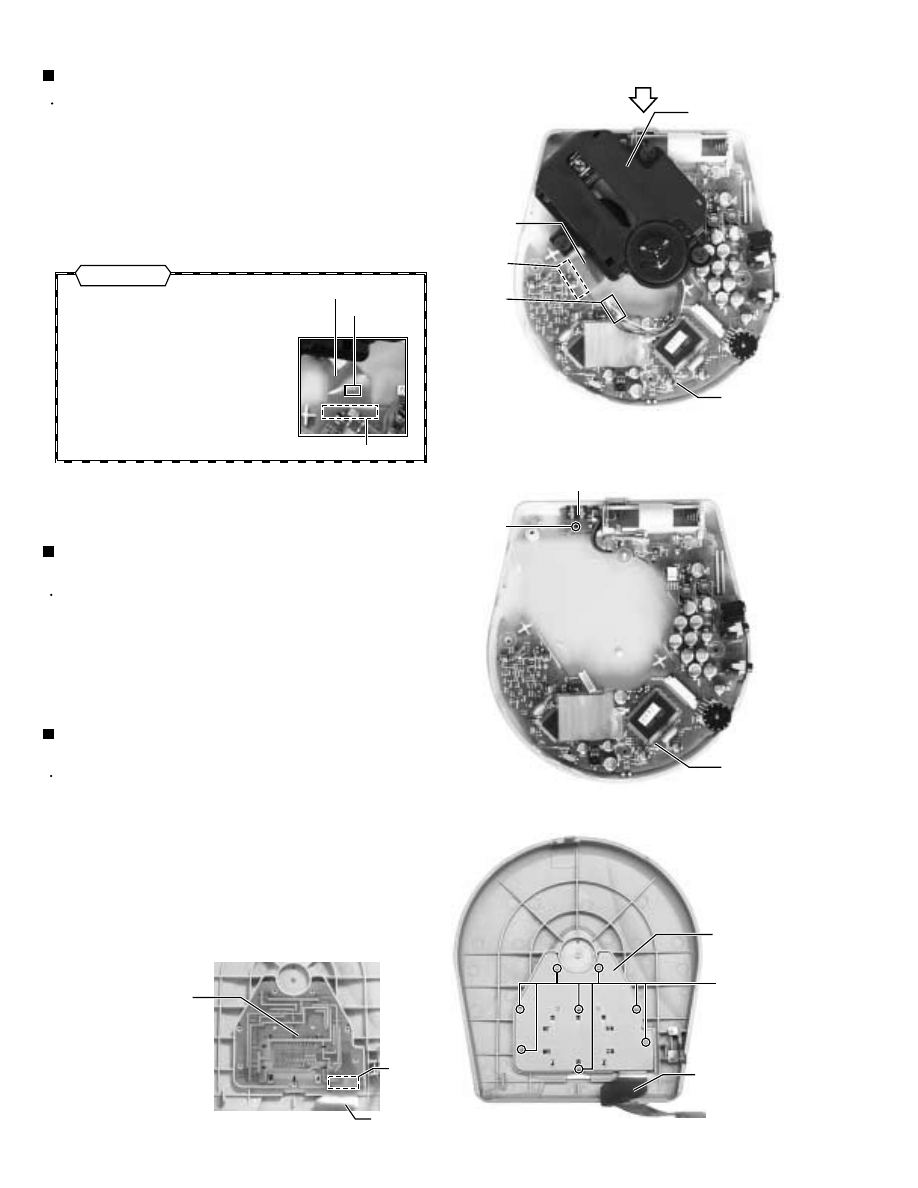
Prior to performing the following procedure, remove
the cabinet -door, cabinet -middlet and CD
mechanism.
Remove the screw D attaching the EXT battery
termial board, and remove the main board with the
EXT battety terminal board.
1.
Removing the main board & EXT battery
terminal board (See Fig.6)
Prior to performing the following procedure, remove
the cabinet -door and cabinet -middle.
Disconnect the harness(motor) from connector
CON2(MOW000) on the main board .
Disconnect the flexible board(pick-up) from
connector CON1 on the main board and remove the
CD mechanism.
ONE POINT :
1.
2.
Removing the CD mechanism (See Fig.5)
Solder the short-circuit land on the
flexible board, before the flexible
board is removed from connector
OCN1 on the main board.
When reassembling, unsolder the
short-circuit land on the flexible
board after connecting the flexible
board.
Flexible board is bonded with a
couple-face tape on the bottom
cabinet.
Prior to performing the following procedure, remove
the cabinet -door and cabinet -middle.
Remove the eight screws E attaching the metal
cover (Peel off the warning label if necessary).
Remove the metal cover and system control board.
Disconnect the flexible board from connecter CON4
on the system control board.
1.
2.
3.
Removing the system control board
(See Fig.7a and 7b)
Flexible board
Short-circuit
land
CON1
(Note : See page 1-4)
Fig.5
Fig.6
Fig.7a
Fig.7b
D
E
CON2
(MOW000)
CD mechanism
Main board
Cabinet -bottom
(inside)
Cabinet -bottom(inside)
EXT battery terminal board
Main board
Flexible board
CON1
Cabinet -door (inside)
Cabinet -door (inside)
Metal cover
System control
board
(Display board)
CON4
Flexible board
Flexible board
Attention
XL-PM11/XM-PM1
1-7
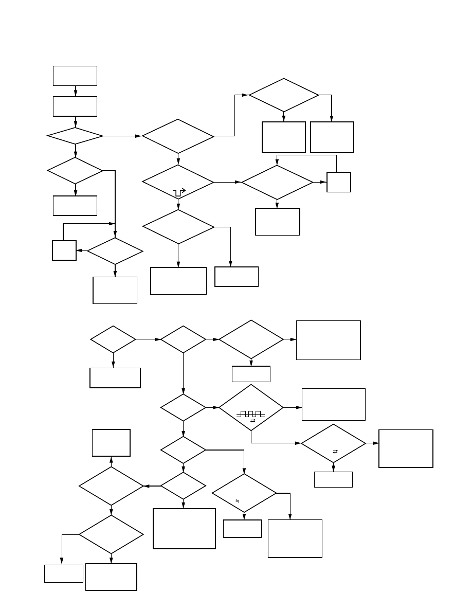
1. POWER / KEY
2. PLAY
1) EXT. DC SUPPLY (ADAPTOR)
2) HOLD S/W in OFF POSITION.
3) CD-DOOR Closed.
REPLACE MICOM
& MAIN PCB
ASS'Y
POWER OFF
(STAND-BY)
'PLAY'
PRESSED
TOC READ
'PLAY'
RE-
ASS'Y
RE-
ASS'Y
REPLACE
XT701
REPLACE
IC6367
& MAIN PCB
ASS'Y
REPLACE
ADAPTOR
& MAIN PCB
ASS'Y
REPLACE
FRONT PCB
ASS'Y
REPLACE LCD
& FRONT PCB
ASS'Y
LCD LIGHT?
COMPLETE
DISPLAY?
CHECK
CONNECTOR
CHECK VOLTAGE
EMITTER of Q102
;3.3V?
CHECK OSC.
of XT701
-3.58MHz?
CHECK VOLTAGE
PIN NO. 11,12,13,18,56
of MICOM
;5V?
CHECK
VOLTAGE WAVEFORM
PIN NO.25 of MICOM
CHECK
CONNECTOR
-COMPLETE?
Yes
Yes
Yes
Yes
Yes
Yes
Yes
Yes
Yes
Yes
Yes
Yes
Yes
Yes
Yes
Yes
Yes
Yes
Yes
No
No
No
No
No
No
No
No
No
No
No
No
No
No
No
No
No
No
No
TOC READ
-PLAY?
CHECK ALL KEY
FUNCTION
CHECK
ASP(9226)
CIRCUIT
CHECK
VOLTAGE PIN No.24
of IC9226
;DC LEVEL
CHECK
VOLTAGE PIN No.1,2
of CON2
;DC LEVEL
CHECK
VOLTAGE PIN No.2,3
of CON1
0.5V 3V
CHECK
VOLTAGE CONNECTOR
PIN of Q301
2V?
CHECK
VOLTAGE PIN No.4,5
of CON2
;DC LEVEL
CHECK
DRIVE IC(6508)
CIRCUIT
CHECK
DRIVE IC 6508
& REPLACE
MAIN PCB ASS'Y
REPLACE
CD-MECHA
REPLACE
CD-MECHA
REPLACE
CD-MECHA
REPLACE
CD-MECHA
MOVE
SLIDE
INSIDE?
PICK-UP
LENS UP/DOWN?
LASER LIGHT?
DISC
ROTATE?
CHECK
ASP(9226),
DSP(9288) CIRCUIT
& REPLACE MAIN
PCB ASS'Y
CHECK
ASP(9226),
DSP(6508) CIRCUIT
& REPLACE MAIN
PCB ASS'Y
CHECK
ASP(9226) CIRCUIT
& REPLACE MAIN
PCB ASS'Y
CHECK
ASP CIRCUIT
REPLACE MAIN
PCB ASS'Y
CHECK
VOLTAGE PIN
No.32 of IC9226 AFTER
PUSH 'PLAY'
(0.5V 3V)
Troubleshooting
XL-PM11/XM-PM1
1-8
Yes
Yes
Yes
Yes
Yes
No
No
No
No
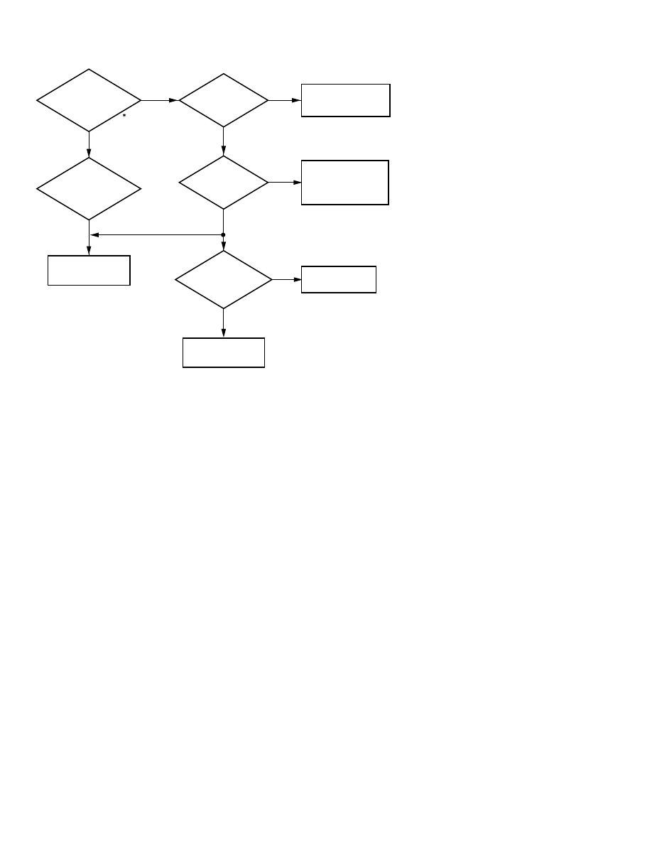
3. AUDIO OUTPUT (LINE OUT, EARPHONE OUT)
CHECK
SIGNAL WAVEFORM
PIN No. 33,38 of IC9288
DURING PLAY STATE.
;AUDIO SIGNAL?
CHECK
SIGNAL WAVEFORM
PIN No. 1,2 of
EARPHONE JACK
;AUDIO SIGNAL?
REPALCE
EARPHONE JACK
REPALCE
LINE OUT JACK
CHECK
VOLTAGE PIN No. 58
of MICOM
; 0V(LOW)
CHECK
VOLTAGE COLLECTOR
PIN of Q803
; 0V(LOW)
CHECK
SIGNAL WAVEFORM
PIN No. 1,2 of LINEOUT JACK
; AUDIO SIGNAL
REPLACE MICOM
& MAIN PCB ASS'Y
CHECK MUTE
CRCUIT & REPLACE
MAIN PCB ASS'Y
REPLACE
MAIN PCB ASS'Y
ANALOG VR
; MAX
Explanation of MP3
An audio compression format that is part of the MPEG-1 specification, which was standardized by the Moving Picture
Experts Group, a working group of ISO (International Organization for Standardization), in 1992.
MPEG-1, which is used by VideoCDs, etc., refers to the international standard for audio/video compression technology and
its format. The audio part of the standard is known as MPEG-1Audio (ISO/IEC 11172-3).
MPEG-1 Audio is an audio coding system that can efficiently compress sound by discarding frequencies below the range of
human hearing(1), as well as sound which is masked(2). MPEG-1Audio is divided into three layers: Layer 1, Layer 2 and
Layer 3. The higher the Layer number, the higher the compression rate and the better the sound quality.
32 kHz, 44.1 kHz and 48 kHz sampling rates are supported. Monaural and 2-channel stereo can be compressed to 32-448
kbps with Layer 1, 32-384 kbps with Layer 2 and 32-320kbps with Layer 3.
The following is a summary of each Layer:
MP3 (MPEG-1 Audio Layer 3)
Layer 3
To create efficiently compressed audio data that is perceptually the same as the original, the following modes have been added to
Layer 2.
MDCT (Modified Diskrete Cosine Transform) for subdivision of bandwidth.
Huffman coding that assigns the short bit to the data that frequently appears, and the long bit to the data that does not appear
much.
MS (Middle/Side) stereo coding(3) that divides the stereo signal into the sum signal (L+R) and the difference signal (L-R).
(1) The human ear cannot detect sound above or below 3 kHz in the silent situation.
(2) Auditory masking is the phenomenon where low-frequency sound that occurs immediately after a loud sound cannot be heard
by the human ear.
(3) Joint stereo coding that compresses 2 channels separately or recognizes only the scale factor of each channel that is
compressed by monaural encoding is used in Layer 1 and 2.
XL-PM11/XM-PM1
1-9
1K
20K
20K
1K
20K
20K
3.75K
20K
20K
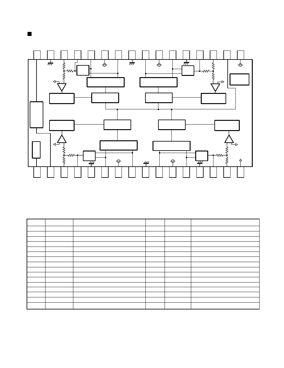
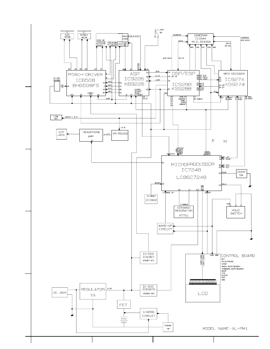
1. Block diagram
BH6508FS (IC6508) : Motor driver
Description of major ICs
1 2 3 4 5 6 7 8 9
1 0 1 1 1 2 1 3 1 4 1 5 1 6
32 31 30 29 28 27 26 25 24 23 22 21 20 19 18 17
- +
- +
- +
- +
2. Pin function
Pin No.
1
2
3
4
5
6
7
8
9
10
11
12
13
14
15
16
Symbol
MUTE 4
CT
IN 1
CN 1
POWGND 1
OUT_IF
POWVCC 1
OUT_1R
POWGND12
OUT_2R
POWVCC2
OUT_2F
POWGND 2
CN 2
IN 2
VREF
Function
Mute terminal
Triangular wave output terminal
CH1 Control signal input terminal
CH1 Feedback filter terminal
Ground for power and analog block
CH1 Non-inverted output terminal
Vcc for power block
CH1 Inverted output terminal
Ground for power block
CH2 Inverted output terminal
Vcc for power block
CH2 Non-inverted output terminal
Ground for power and digital block
CH2 Feedback filter terminal
CH2 Control signal input terminal
Reference voltage input terminal
Pin No.
17
18
19
20
21
22
23
24
25
26
27
28
29
30
31
32
Symbol
VCC
VG
IN3
CN3
POWGND3
OUT_3F
POWVCC3
OUT_3R
POWGND34
OUT_4R
POWVCC4
OUT_4F
CN4
IN4
POWGND4
CLK
Function
Control circuit power supply
Pre-drive circuit power supply
CH3 Control signal input terminal
CH3 Feedback filter terminal
Ground for power block
CH3 Non-inverted output terminal
Vcc for power block
CH3 inverted output terminal
Ground for power block
CH4 inverted output terminal
Vcc for power block
CH4 Non-inverted output terminal
CH4 Feedback filter terminal
CH4 Control signal input terminal
Ground for power block
External clock input terminal
Note: Nin-inverted output and inverted output if driver are the polarity to an input terminal.
NF
Amp.
NF
Amp.
NF
Amp.
NF
Amp.
SAW
OSC
LOGIC 4
LOGIC 1
LOGIC 3
LOGIC 2
H BRIDGE 4
H BRIDGE 1
H BRIDGE 3
H BRIDGE 2
PRE
DRIVER 4
PRE
DRIVER 1
PRE
DRIVER 2
Thermal
shut down
PRE
DRIVER 3
MUTE 4
F R
F R
R F
VG
VREF
CT
CLK
VCC
XL-PM11/XM-PM1
1-10
KS9288 (IC9288) : DSP/ ESP
2. Pin function
(1/2)
Symbol
VDD_PLL
VSSA_PLL
VBBA_PLL
VCO1LF
VCO2LF
VSSD_PLL
VDDD_PLL
PBCK
VDDD1
XIN
XOUT
VSSD1
TEST0
EFMI
LOCK
SMEF
SMON
SMDP
SMDS
WDCK
VDDD2
TESTV
WFCK
LKFS
RESETB
MLT
MDAT
MCK
ISTAT
S0S1
SQCK
SQDT
LCHOUT
VDDA_DAC
VHALF
VREF
VSSA_DAC
RCHOUT
VDDD_DAC
VSSD_DAC
TEST1
TEST2
TEST3
MUTE
SBCK
SBDT
C4M
VSSD2
VDDD3
DATX
JITB
C2PO
1~20
21~40
41~60
80~61
1.Pin layout
Pin No.
1
2
3
4
5
6
7
8
9
10
11
12
13
14
15
16
17
18
19
20
21
22
23
24
25
26
27
28
29
30
31
32
33
34
35
36
37
38
39
40
41
42
43
44
45
46
47
48
49
50
51
52
I/O
-
-
-
O
O
-
-
-
-
I
O
-
I
I
O
O
O
O
O
O
-
I
O
O
I
I
I
I
O
I/O
I
O
O
-
O
O
-
O
-
-
I
I
I
I
I
I/O
O
-
-
O
I/O
I/O
Function
Analog Power for DPLL
Analog Ground for DPLL
Analog Bulk Bias Ground for DPLL
Pump out for VCO1
Pump out for VCO2
Digital Ground Separated Bulk Bias for DPLL
Digital Power Separated Bulk Bias for DPLL
VCO1/2 clock output (4.3218MHz)
Digital Power
X'tal oscillator input (16,9344MHz)
X'tal oscillator output
Digital Power
Test input
EFM signal input
CLV Servo locking status output
LPF time constant control of the spindle servo error signal
ON/OFF control signal for spindle servo
Phase control output for Spindle Motor drive
Speed control output for Spindle Motor drive
Word clock output (X1: 88.2KHz, X2: 176.4KHz)
Digital Power
Various Test input
Write base clock output
The Lock status output of frame sync
System Reset at 'L'
Latch signal input from Micom
Serial data input from Micom
Serial data receiving clock input from Micom
The internal stats output to Micom
Subcode sync signal (S0+S1) output
Subcode-Q data transferring bit clock input
Subcode-Q data serial output
Left-Channel audio output through DAC
Analog Power for DAC
Reference Voltage output for bypass
Reference Voltage output for bypass
Analog Power for DAC
Right-Channel audio output through DAC
Digital Power for DAC
Digital Ground for DAC
Test Input
Test Input
Test Input
System mute at 'H'
Subcode data transferring bit clock
Subcode data serial output
4.2336MHz clock output
Digital Ground
Digital Power
Digital audio data output
Internal SRAM filter margin status output
C2 Pointer output
XL-PM11/XM-PM1
1-11
3. Block diagram
DPLL
CLV
Servo
Timing
Generator
Micom
Interface
Subcode
Out
EFM
Demodulator
ECC
16K
SRAM
Address
Generator
Interpolator
Digital
Out
I/O
Interface
Encoder
Decoder
DRAM
Interface
Digital
Filter
1-bit
DAC
PWM
LPF
SQCK
SBCK
S0S1
SQDT
SBDT
C2HO
DAIX
VHALF
VREF
LCHOUT
RCHOUT
AD9 - AD0
D3 D0
CAS1- CAS0
RAS
WE
JITB
VCO1LP
VCO2LP
EFMI
LOCK
SMLT
SMON
SMDP
SMDS
WDCK
TESIV
WFCK
RFCK
C4M
XIN
ISIAI
MLL
MDAL
MCK
MUTE
Pin No.
53
54~59
60
61
62
63
64
65
66
67
68
69
70
71
72
73
74
75
76
77
78
79
80
Symbol
RFCK
MNT0~5
VSSD3
VDDD4
D0
D1
WE
RAS
D2
D3
CAS0
CAS1(AD10)
AD8
AD7
AD6
AD5
AD4
AD9
AD0
AD1
AD2
AD3
VSSD4
I/O
I/O
I/O
-
-
I/O
I/O
O
O
I/O
I/O
O
O
O
O
O
O
O
O
O
O
O
O
-
Function
Read base clock output
Monitoring signal output
Digital Ground
Digital Power
DRAM data Input/Output 0
DRAM data Input/Output 1
DRAM Write Enable output (active Low)
DRAM Row Address Selection output (active Low)
DRAM data Input/Output 2
DRAM data Input/Output 3
DRAM Column Address Selection output 0 (active Low)
DRAM Column Address Selection output 1 (active Low)
DRAM Address output 8
DRAM Address output 7
DRAM Address output 6
DRAM Address output 5
DRAM Address output 4
DRAM Address output 9
DRAM Address output 0
DRAM Address output 1
DRAM Address output 2
DRAM Address output 3
Digital Ground
2. Pin function
(2/2)
XL-PM11/XM-PM1
1-12
1. Block diagram
M11L1644 (IC1644) : DRAM
2. Pin function
Pin No.
3~11, 14~19, 7
5
21
4
20
2, 3,22, 23
1, 12
13, 24
6
Symbol
A0~A10
RAS
CAS
WE
OE
I/O0~I/O3
Vcc
Vss
NC
Function
Address Input
Row Address : A0~A10
Column Address : A0~A10
Row Address Strobe
Column Address Strobe
Write Enable
Output Enable
Data Input/ Ountput
Power (5V or 3.3V)
Ground
No Connect
11
11
11
11
11
4
4
4
CONTROL
LOGIC
CLOCK
GENERATOR
COLUMN
ADDRESS
BUFFER
REFRESH
CONTROLLER
REFRESH
COUNTER
ROW
ADDRESS
BUFFERS(11)
DATA-IN BUFFER
DATA-OUT
BUFFER
COLUMN
DECODER
SENSE AMPLIFIERS
I/O RATING
2048 x 4
2048 x 2048 x 4
MEMORY
ARRAY
ROW
DECODER
Vdd GENERATOR
2048
2048
WE
RAS
CAS
A0
A1
A2
A3
A4
A5
A6
A7
A8
A9
A10
I/O0
..
I/O3
CE
Vcc
Vss
I/O
I
I
I
I
I
I/O
-
XC6367 (IC6367, 63670) : Regulator
5
4
1
2
3
1. Pin layout
1
2
3
4
5
Pin
No.
Symbol
EXT
GND
CE
VDD
VOUT
Function
2. Pin function
External transistor connection
Ground
Chip enable
Power supply
Voltage output
XL-PM11/XM-PM1
1-13
Parts list
CD mechanism assembly
(See page 1-15)
Lid -battery
(See page 1-16)
Knob -hold
(See page 1-16)
Holder -battery
(See page 1-16)
Integrated decomposition chart
Cabinet -door assembly
(See page 1-14)
Cabinet -middle assembly
(See page 1-14)
Cabinet -bottom assembly
(See page 1-16)
Block No.
M
M
M
1
Main board assembly
(See page 1-15)
XL-PM11/XM-PM1
1-14
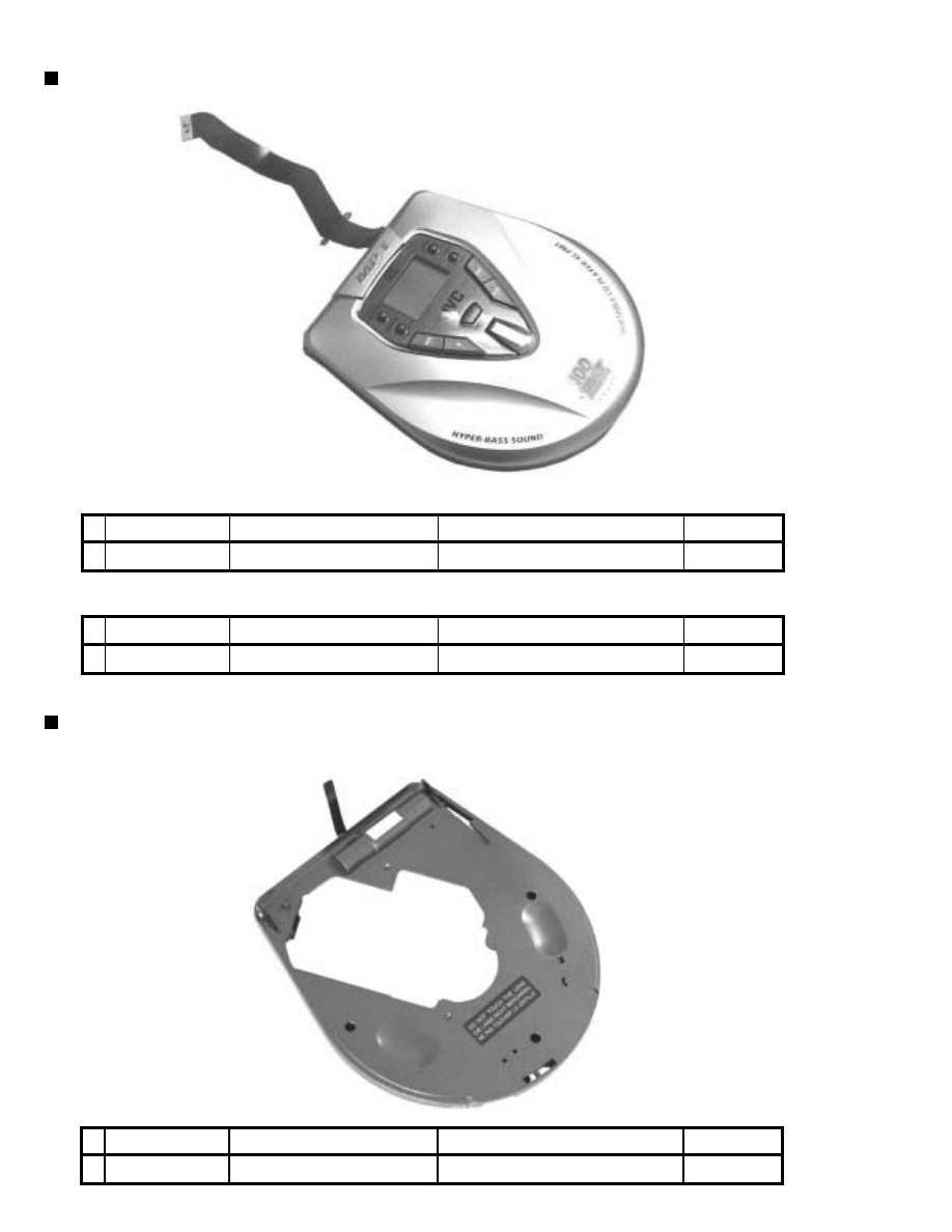
Cabinet -door assembly
Parts number
AH64-01527A
Parts name
CABINET -DOOR
Description
WITH FRONT BOARD
Cabinet -middle assembly
Parts number
AH64-01528A
Parts name
CABINET -MIDDLE
Description
WITH RIBBON
Area suffix
ALL
Parts number
AH64-01527B
Parts name
CABINET -DOOR
Description
WITH FRONT BOARD
Area suffix
C
Area suffix
ALL
(XL-PM11C)
(XL-PM1)
XL-PM11/XM-PM1
1-15
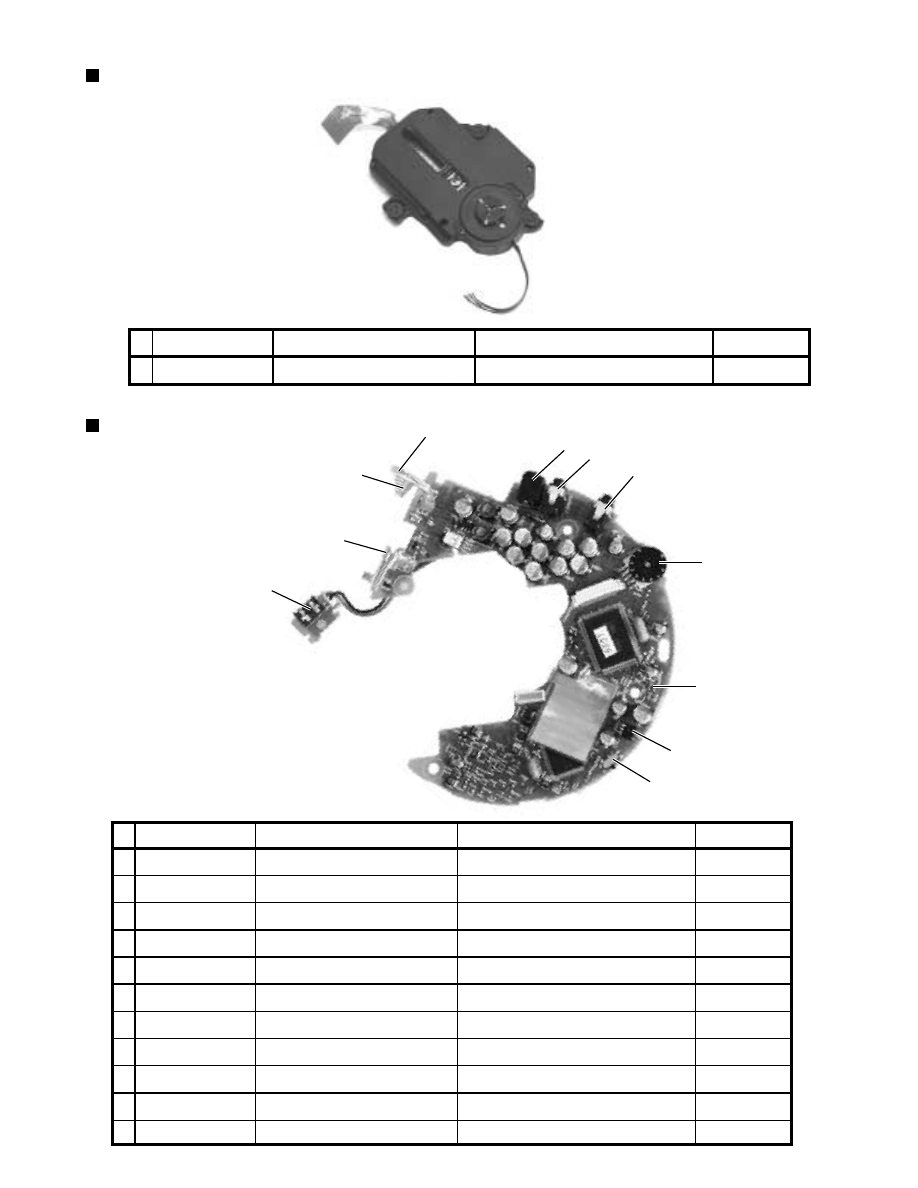
Main board assembly
2
1
2
3
4
5
6
7
8
9
10
11
Parts number
AH92-01161A
2102-001063
3408-001038
3409-001004
3722-001525
3722-001525
3722-001493
AH61-00595A
AH61-00600A
AH61-00594A
3710-001696
Parts name
MAIN BOARD ASSY
VR -ROTARY
SWITCH -SLIDE
SWITCH-DETECTOR
JACK -DC POWER
JACK -LINE OUT
JACK -PHONE
BRACKET -BATTERY.P
SPRING -BATTERY
BRACKET-CHARGER
CONNECTOR - SOCKET
Description
PCB MAIN
VOLUME
HOLD S/W
DOOR - S/W
Area suffix
ALL
ALL
ALL
ALL
ALL
ALL
ALL
ALL
ALL
ALL
ALL
3
1
4
7
5
6
9
8
10
11
CD mechanism assembly
Parts number
AH59-00968A
Parts name
CD MECHANISM ASSY
Description
MECH+ RUBBER CD
Area suffix
ALL
XL-PM11/XM-PM1
1-16
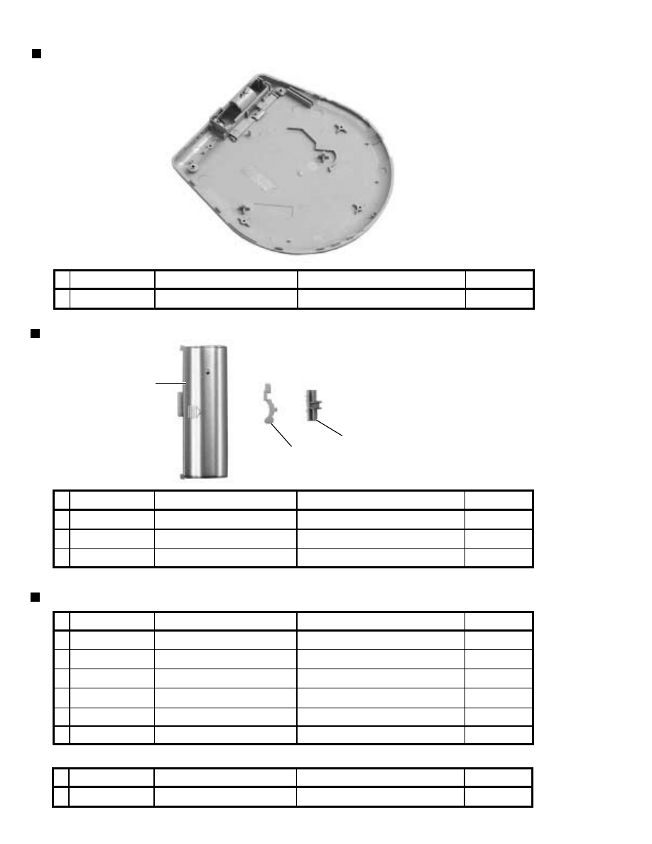
Other parts
1
2
3
Parts number
AH68-50482B
AH68-00875A
AH68-00875B
AH68-00875D
AH68-50275D
AH68-00907A
Parts name
LABEL -CLASS 1
LABEL -RATING
LABEL -RATING
LABEL -RATING
LABEL -WARNING
LABEL -DHHS
Description
BOTTOM SIDE
BOTTOM SIDE
BOTTOM SIDE
BOTTOM SIDE
CABINET -MIDDLE INSIDE
BOTTOM SIDE
Area suffix
B, E
J, C
E
B
B, E
J, C
Parts number
AH64-01021A
AH61-00734A
AH64-01029A
Parts name
LID -BATTRY
HOLDER -BATTERY
KNOB -HOLD
Description
BATTERY -COVER
Area suffix
ALL
ALL
ALL
Labels
Cabinet -bottom assembly
Parts number
AH64-01529A
Parts name
CABINET -BOTTOM
Description
WITH BATTERY COVER
Area suffix
ALL
Parts number
AH68-00875C
Parts name
LABEL -RATING
Description
BOTTOM SIDE
Area suffix
C
1
2
3
(XL-PM11C)
Does not contain
the bottom side label.
XL-PM11/XM-PM1
1-17
A3
A1,A6 to A9
A2
P1
P1
P2
A5
FR
ONT
P3
P4
A4
Gift box (XL-PM11C/ XL-PM1B/ XL-PM1E)
Packing materials and accessories parts list
Block No.
M
M
M
3
Block No.
M
M
M
5
Blister (XL-PM1J/ XL-PM1C)
No do after-sales service of blister pack packing.
Parts name
PE-BAG
PAD-CUSHION
PACKING-CASE
PACKING-CASE
LABEL-GIFT BOX
Parts number
AH69-00359A
AH69-00538A
AH69-00538B
AH69-00538C
AH68-00930A
Description
HDPE
SW-1
SW-1
SW-1
ART PAPER
Q'ty
2
1
1
1
1
Area
ALL
11C, B, E
11C
B, E
11C, B, E
Item
P1
P2
P3
P4
Parts list (Packing)
Block No. M3MM
XL-PM11/XM-PM1
1-18
Parts name
INSTRUCTIONS
INSTRUCTIONS
INSTRUCTIONS
CASE-BATTERY
HEAD-PHONE
EAR-PHONE
AC-ADAPTER
AC-ADAPTER
AC-ADAPTER
WARRANTY CARD
WARRANTY CARD
WARRANTY CARD
SVC LIST
S.INST SHEET
S.INST SHEET
REGISTRATION CARD
Parts number
AH68-00944C
AH68-00944E
AH68-00944D
AH64-01082A
AH30-00016A
AH30-00015A
AH44-00022A
AH44-00021A
AH44-00020A
BT-51626-1
BT-52004-1
BT-54008-2
BT-20071B
BT-20044G
E43486-340B
BT-51020-2
Description
EN/FR
EN/SP/NL/GE/IT/
FR/SW/FI/DA
EN
ASSY
OVER HEAD
INNER EAR
AA-R4510
AA-R4511
AA-R4512
Q'ty
1
1
1
1
1
1
1
1
1
1
1
1
1
1
1
1
Area
C, 11C
E
J, B
ALL
J, C, 11C
B, E
J, C, 11C
E
B
J
C
B, E
C
J
B
J
Item
A1
A2
A3
A4
A5
A6
A7
A8
A9
Parts list (Accessories)
Block No. M5MM

XL-PM11/XM-PM1
1-19
< M E M O >

200107(V)
VICTOR COMPANY OF JAPAN, LIMITED
PERSONAL & MOBILE NETWORK BUSINESS UNIT. 10-1,1chome,Ohwatari-machi,Maebashi-city,371-8543,Japan
(No.21018)
XL-PM11/XL-PM1
XL-PM11/XL-PM1
2-1
1
2
3
4
5
A
B
C
D
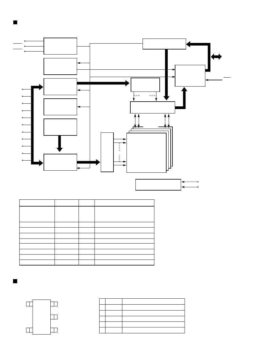
Block diagram
A
B
C
D
E
F
G
1
2
3
4
5
2-2
XL-PM11/XL-PM1
Standard schematic diagram
CD signal
ASP
16MDRAM
DSP/ESP
MP3 DECODER
MICROPROCESSOR
M. DRIVER
HP AMP.
No. VA-00-5420
SUBJECT :
Part number change
Date : 23
th. JUL. 2001
A. To improve performance. E. Standardization of part.
B. To improve reliability.
F. For your demand.
C. To improve safety.
G. Correction of misprint.
D. To improductivity
H. Others.
A. Completely interchangeable.
B. Previous part can be used for new set,but new
part can not be used for previous set.
C. New part can be used for previous set,but
previous part can not be used for new set.
D. Not interchangeable.
E. Addition
F. Deletion
COMMENTS :
Model & Manual No.
XL-PM11/XL-PM1
J/C/B/E
(No.21018)
Location
Parts list
Reference Information
------
Performed at factory
#1~
Page
Parts No.
Parts Name
FOB
(New Parts)
Itg
Rsn Note
D G
The following parts have been changed. Please note these new parts in your service manual.
We suggest that you order the parts concerned as apares.
Parts identified by the symbol are critical for safety. Replace only with specified part numbers.
----
3722-001493
Jack Line out
1-15
ATTACHMENT
( ) NONE ( ) COMPONENT / PWBLAYOUT
( ) SCHEMATIC DIAGRAM ( ) ADJUSTMENT PROCEDURE
( ) EXPLODED VIEW
x
CD-ROM No.
SML200107
Old parts
3722-001525
Item
Main Board
assembly
#6
VICTOR COMPANY OF JAPAN,LTD,
AV & MULTIMEDIA COMPANY
AUDIO & COMMUNICATION BUSINESS DIV.
1-10-1,Ohwatari-chou. Maebashi-shi,Gunma-ken.371-8543, Japan Facsimile : 81-27-254-8977 Telephone : 81-27-254-8952
QUALITY ASSURANCE DEPARTMENT
SERVICE ENGINEERING GROUP 15300
INTERCHANGEABILITY
REASON FOR CHANGE
Document Outline
Wyszukiwarka
Podobne podstrony:
Jvc Zero 5 Service Manual
Jvc Zero 9 Service Manual
Jvc VS 5313 Service Manual
Jvc VS 5313 Mk2 Service Manual
Jvc XVS 500 BK Service Manual 3
Jvc VSDT 2000 Service Manual
Jvc XMD 88 GD Service Manual 2
Jvc XM 448 BK Service Manual
Jvc XVM 557 GD Service Manual 2
hplj 5p 6p service manual vhnlwmi5rxab6ao6bivsrdhllvztpnnomgxi2ma vhnlwmi5rxab6ao6bivsrdhllvztpnnomg
Oberheim Prommer Service Manual
Korg SQ 10 Service Manual
MAC1500 service manual
Kyocera Universal Feeder UF 1 Service Manual
Proview RA783 LCD Service Manual
indesit witp82euy Service Manual
Glow Worm installation and service manual Hideaway 70CF UIS
Proview PZ456 LCD Service Manual
Glow Worm installation and service manual Ultimate 50CF UIS
więcej podobnych podstron