
Digital Control of Switching Power Supply
- Power Factor Correction Stage
Sangsun Kim and Dr. P. Enjeti
Power Electronics and Power Quality Laboratory
Department of Electrical Engineering
Texas A&M University
College Station, TX – 77843-3128
Tel: 979-845-7466
Fax: 979-845-6259
Email:
enjeti@ee.tamu.edu
Abstract: Industry standard for the control of switch mode power supply (SMPS) systems has been
analog control. Now with the advent of high speed, lower cost digital signal processing (DSP) ICs,
digital control there has been an increased interest in digital control of SMPS. The Power
Electronics & Power Quality Laboratory of Texas A&M University is currently exploring several
implementation aspects of digital control of power factor correction (PFC) stage of SMPS. Two low
cost digital controllers: TMS320LF2407 and ST52x420 are evaluated for implementing PFC
function. Simulation and experimental results are shown to demonstrate PFC control of SMPS to
meet IEC 1000-3 harmonic limits.
I.
Introduction
Worldwide, the markets of internal and external switch mode ac/dc power supply (SMPS) have
been growing at a faster rate for several applications such as communications, computers,
instrumentation, Industrial controls, and military/aerospace area [1, 2]. According to resent
estimates, the world wide SMPS market share for power supplies (notebook computer, cellular
phone, modem, and telecommunication equipment) is expected to increase from about $20 billion
in 2000 to $56 billion by 2005, for a compound annual growth rate 23.2 %. The majority of the
present day SMPS employ analog control and are undergoing slow evolution. On the other hand,
enabling technologies such as digital signal processors (DSP), integrated semiconductors,
magnetics, improved power components, and cooling technologies are fast evolving. Tomorrow’s
SMPS is expected to be highly efficient, with near unity power factor, DSP control, 10W per cubic
inch, and 400+A in the same size as 200A today. In response to the concerns, this article evaluates
the feasibility employing state of the art digital control of power factor correction stage with fuzzy
logic algorithm.

A conventional SMPS employs a diode rectifier for ac to dc conversion. This type of utility
interface generates harmonics and the input power factor (PF) and total harmonic distortion (THD)
are poor. IEC 1000-3 and IEEE 519 standards specify link as harmonic compliance and THD. To
comply with the corresponding standards in Europe and North America several active solutions
have been proposed [2] and widely studied in the literature, being most usually employed the boost
converter. The design of the switching power supply requires many features such as:
1. Lower input current harmonics to meets the IEC 1000-3 harmonic limits.
2. High input power factor to minimize reactive requirements.
3. Minimum conducted EMI.
Up to now, the demands for digital processor have been increased due to its low cost, high speed
operation, and flexibility. In this article, several implementation aspects of digital control of power
factor correction (PFC) stage of SMPS are explored. 16-bit fixed point DSP, TMS320LF2407, is
evaluated for implementing PFC function. To further reduce the cost and implement fuzzy logic
control for PFC, 8-bit micro-controller, ST52x420, is employed. Simulation and experimental
results are shown to demonstrate PFC control of SMPS to meet IEC 1000-3 and IEEE 519 harmonic
limits.
II. Analog and Digital Control
Traditionally, the imple mentation of switching power supply has been accomplished by using
analog power factor correction (PFC) as shown in Fig. 1 [3]. Analog PFC IC's which are
manufactured by TI/Unitrode, Fairchild, and STmicroelectronics are available and have been able to
provide improved power factor. Analog control can provide continuous processing of signal, thus
allowing very high bandwidth. It also gives infinite resolution of the signal measured. Analog
control, however, also posses some drawbacks such as a number of parts required in the system and
their susceptibility to aging and environment variations, which lead to high cost of maintenance.
Further, analog control once designed is inflexible and performance cannot be optimized for various
utility distortions. In the view of these, this article explores digital implementation of switch mode
power supply via digital control. Digital control provides advantages such as programmability, less
susceptibility to environmental variations, and fewer part counts [2]. It also reduces the size of the
power supply by containing the complexity of control system within the software. Therefore, since
digital control is much flexible than analog control, is becoming lower cost, and applicable for
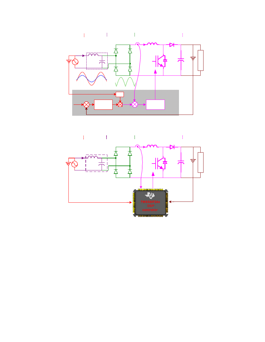
Utility
LC filter
Diode Rectifier
Boost Converter
Load
+
_
L
o
a
d
+
_
V
i
V
S
i
S
L
S
C
S
i
dr
L
dr
V
dr
C
dc
V
dc
V,i
Voltaage
Regulator
| |
+
_
Current
Regulator
+
_
Gate input
*
d r
i
*
dc
V
D
i
dr
V
dc
Analog IC
:
UC3854(TI/Unitrode), ML4812(Fairchild), L6561(STM)
Fig. 1 Power factor corrected boost converter with analog control.
Utility
LC filter
Diode Rectifier
Boost Converter
Load
+
_
L
o
a
d
+
_
V
S
i
S
L
S
C
S
i
dr
L
dr
V
dr
C
dc
V
dc
Gate input
D
i
dr
V
dc
V
S
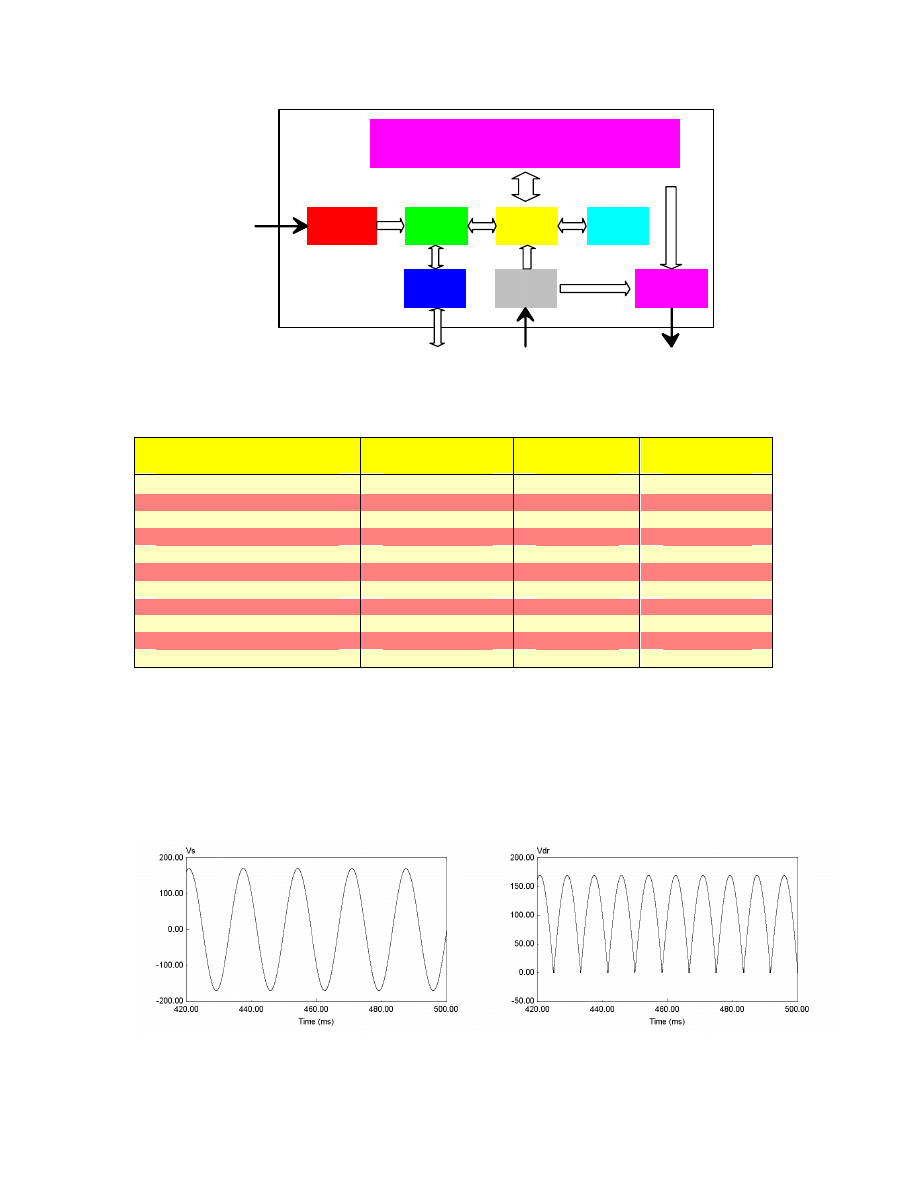
DSP Control
Fig. 2 Digital control of PFC Boost Converter.
intelligent control, it can be employed for power supply applications as shown in. Fig. 2. In order to
obtain high speed bandwidth of the fixed point DSP, TMS320LF2407, numerous off-line
computations are first performed and the outputs of the controller based on fuzzy logic rules are
stored in a memory block. Further low cost implementation on an 8-bits micro-controller,
ST52x420, along with ST-Fuzzy Studio is explored and achieved.
III. Operation Concept and Analysis
Normally, diode rectifier system contains a lot of harmonic contents such as 3
rd
, 5
th
, 7
th
, etc. as
shown in Fig. 3. To improve the input THD, the additional PFC boost converter in the system is
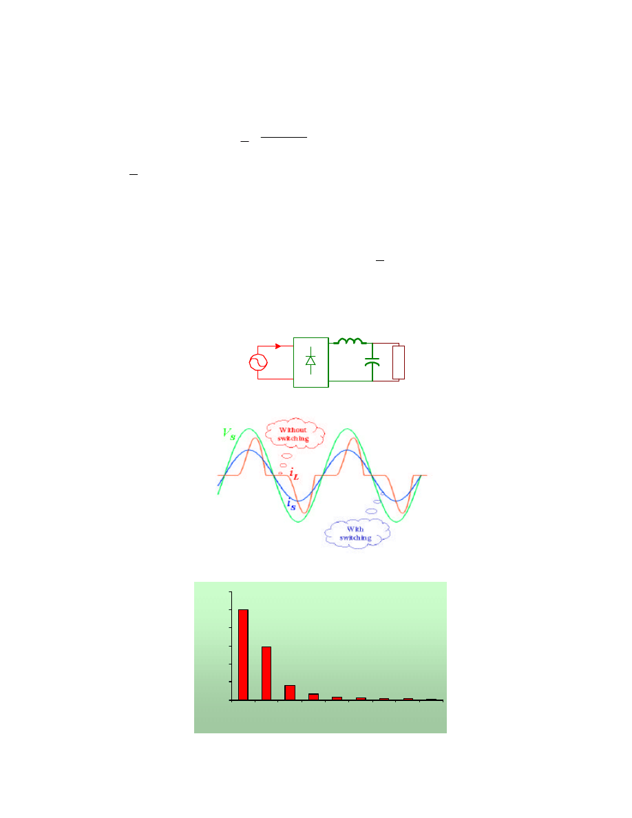
employed. Due to the rectified voltage
d r
V
and the characteristic of diode rectifier current, a
disturbance is considered as,
*
dc
d r
*
dc
V
V
V
D
−−
==
,
(2)
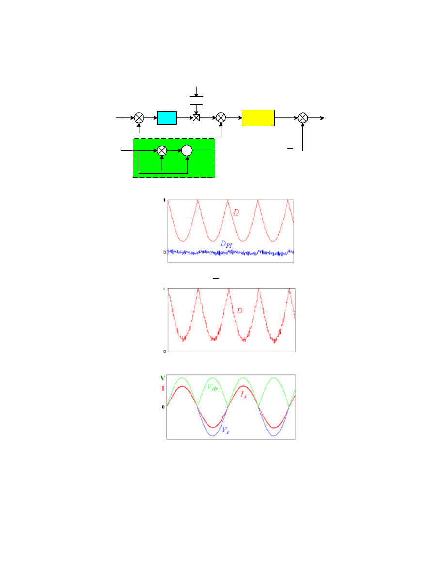
where, D is the duty ratio of the boost converter controlled by open-loop control. The duty ratio
PI
D
by closed loop PI control is obtained from the control block diagram which consists of dc
voltage and current controllers and the disturbance as shown in Fig. 4. Since the duty ratio D
has a
reverse waveform of the rectified voltage
d r
V
to make input current sinusoidal as shown in Fig. 5,
lower and higher harmonic components are obtained from D and
PI
D
, respectively. Therefore,
higher bandwidth of the whole control system can be achieved with lower bandwidth of current PI
controller.
L
o
a
d
V
S
i
L
V
dc
(a) Diode rectifier system
(b) Utility current and voltage
0
0.2
0.4
0.6
0.8
1
1.2
1
3
5
7
9
11
13
15
17
Harmonic order (h )
I
h
/I
1
(c) Harmonics of diode rectifier current
Fig. 3 The concept of power factor correction.
PI
| |
+
_
+
_
PI Current
Regulator
+
+
Duty Ratio
÷÷
Disturbance
t
e
ω
sin
*
d r
i
d r
i
+
_
d r
V
*
dc
V
dc
V
D
D
PI
D
Fig. 4 Control block diagram for the proposed PFC boost converter.
(a)
D
and
PI
D
(b) Duty ratio D
(c) Utility voltage and current
Fig. 5 The waveforms of control system parameters.

IV. Controller Implementation
The proposed control system is implemented by using either ST-Fuzzy Studio (ST52x420) or TI
DSP, TMS320LF2407. The features of two digital controllers are shown in Table I. The utility
voltage
s
V
, output dc voltage
dc
V
, and inductor current
d r
i
are sensed through A/D converters. A
gate signal is obtained from PWM channel. The switching frequency for the boost converter is
40[kHz].
A. 16-bit Fixed-point DSP implementation [4]
The proposed PFC approach is implemented on TMS320LF2407 DSP which has a function of 16
bit fixed-point arithmetic and is designed to meet a wide range of digital motor control and other
control applications. This DSP chip comes from the 24x family, which is optimized for control
applications. It has a 30Mhz CPU clock and several peripherals such as Event Manager, CAN
Interface, SPI, SCI, and ADC modules. Fig. 6 illustrates the simplified hardware diagram for the
DSP. The TMS320LF2407 DSP also comes with a flash ROM, allowing it to be reprogrammed for
software updates. The ’240x series of TI DSP controllers combines this real-time processing
capability with controller peripherals to create an ideal solution for control system applications. To
achieve fast real time processing of the fuzzy logic control algorithm, 16k (128
×
128) byte flash
ROM blocks are used with off-line computations based on Fig. 7 [5, 6]. The control loop sampling
frequency for the proposed PFC scheme can be up to 100 [kHz].
ADC channel
TMS320LF2407
DSP Core
Event Manager Module
Ÿ
PWM channels
Ÿ
Timer
30MHz
Clock
Other Modules:
SPI,SCI,CAN
Power device
Flash
ROM
Analog Input
Fig. 6 TMS320LF2407 DSP simplified hardware diagram.
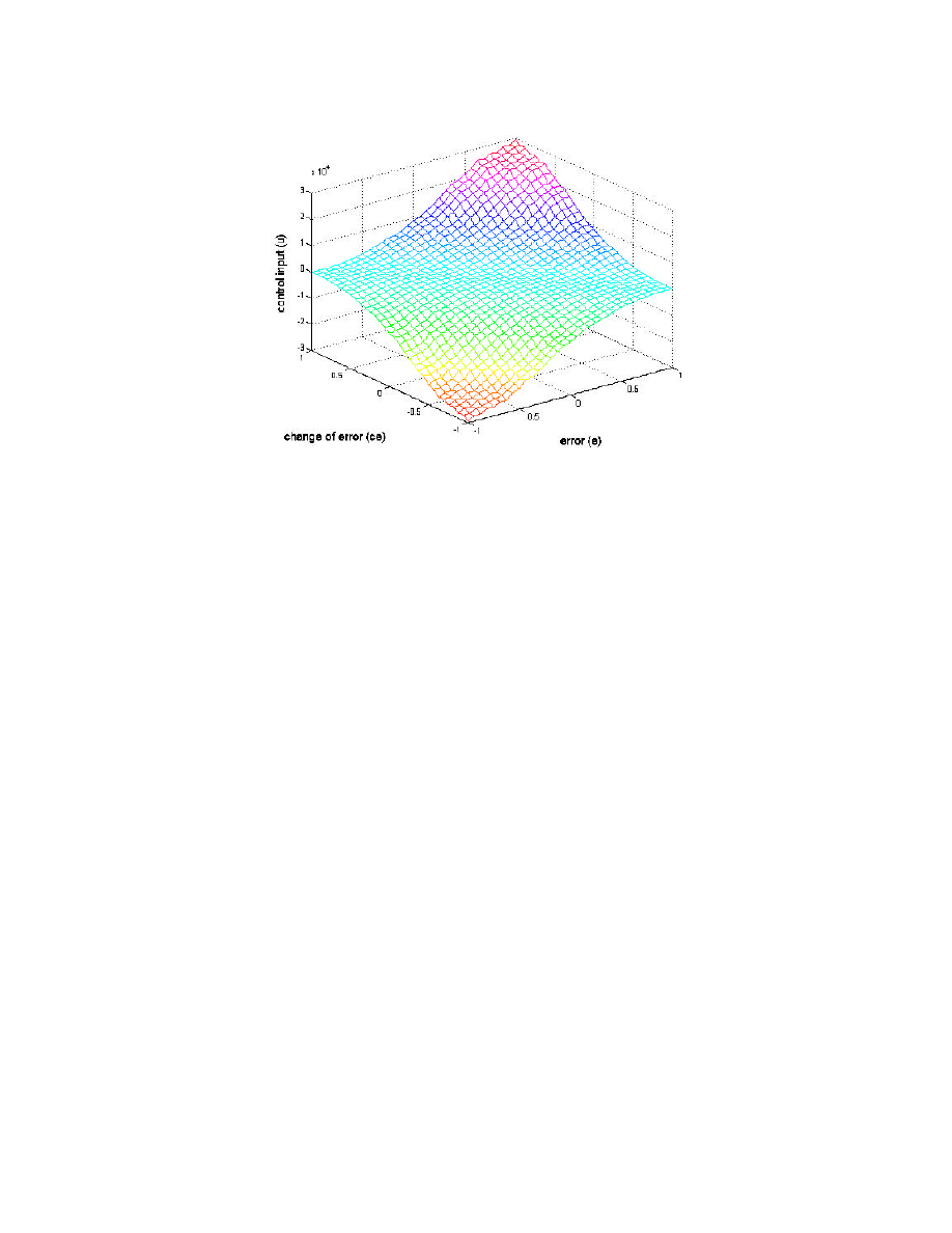
Fig. 7 The output of fuzzy logic controller obtained from off-line computation.
B. 8-bit micro-controller implementation [7]
To achieve further low cost implementation, in this article, ST micro-controller, ST52x420, is
explored. The controller is designed for fuzzy logic implementation for control applications such as
home appliances and industrial controls. ST-Fuzzy Studio block diagram is shown in Fig. 8. The
flexible I/O configuration of ST52x420 allows to interface with a wide range of external devices,
like D/A converters or power control devices. The A/D Converter of ST52x420 is an 8-bit analog to
digital converter with up to 8 analog inputs offering 8-bit resolution and a typical conversion time
of 4.1 us with a 20 MHz clock. ST52x420 is supported by FuzzyStudio allowing to grapically
design a project and obtain an optimized microcode. The control loop sampling frequency for the
proposed PFC scheme can be up to 7.5 [kHz].
A/D
Converter
ST52x420
ALU & FUZZY CORE
I/O
PWM
Channels
4 KBytes
EPROM
Analog
Input
128 Bytes
RAM
Control
UNIT
Watchdog
Fig. 8 ST-Fuzzy Studio (ST52x420) architectural block diagram.
Table I. Comparison of two digital controllers
Feature
TMS320LF2407
ST52x420
Unit
Computational quantity
16
8
Bits
CPU frequency
30
20
Mhz
Memory(ROM)
32k flash
4k EPROM
Bytes
Memory(RAM)
128
2.5k
Bytes
ADC channels/bits
16/10
8/8
Channels/bits
AD conversion time
0.5
4.1
µ
sec
PWM
16
3
Pins
Timer
4
3
Pins
Digital I/O pins
41
19
Pins
Software tool
Code Composer
FuzzyStudio
Price*
5
1
*
The item is approximated price.
V. Simulation and Experimental Results
Simulation results are shown in Fig. 9 and Fig. 10, with and without input voltage distortion
respectively. Fig. 11 shows the experimental results.
(a) Utility voltage
(b) Rectified input voltage
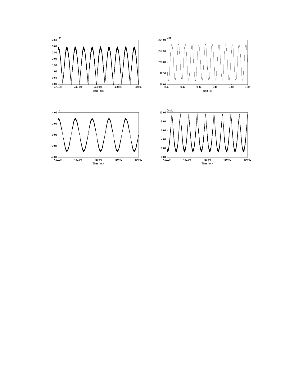
(c) Boost inductor current
(d) Utility current
(e) Dc voltage
(f) Fuzzy logic output (PFC input; D
×
10)
Fig. 9 Simulation results.
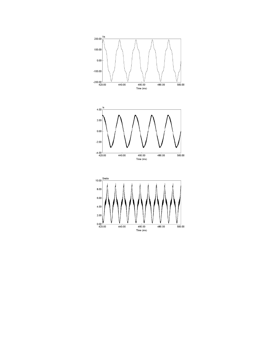
(a) Utility voltage
(b) Utility current
(c) Fuzzy logic output (PFC input; D
×
10)
Fig. 10 Simulation results with utility voltage distortion.
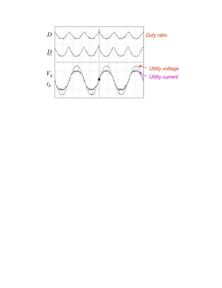
Fig. 11 Experimental results.
V. Conclusions
Several implementation aspects of digital control of power factor correction (PFC) stage of SMPS
have been explored with low cost digital controllers: TMS320C2407 and ST52x420. Strict
harmonic limit such as IEC 1000-3 are here to stay. To meet the limits and come up with growing
ac/dc power supply markets, the PFC stage is currently required. Analog PFC control is the current
industry choice but this type of control is not flexible. Therefore, digital based control has many
advantages with higher performance since the cost of digital controller (due to its usage in many
applications) has the potential to become lower. Higher speed digital controller can guarantee
higher bandwidth and higher switching frequency for ac/dc power supply.
References
[1] Jigna Patel, "The Hottest Markets for External Power Supplies Now ans a Look at Potential Future Markets",
APEC’01, pp. , 2001.
[2] Mark T. Gaboriault, "U.S. Merchant Markets and Applications for Internal AC/DC Switching Power Supplies and
DC/DC Co nverters", APEC’00, pp. 59-63, 2000.
[3] P. C. Todd, “UC3854 Controlled Power Factor Correction Circuit Design,” Application Note U-134, Unitrode
Corporation/ Texas Instruments.
[4] Texas Instruments, TMS320LF/LC240x DSP Controllers Reference Guide: System and Peripherals, 2000.
[5] Bimal K. Bose, "Expert System, Fuzzy Logic, and Neural Network Applications in Power Electronics and Motion
Control," Proceedings of IEEE, vol. 82, No. 8, pp. 1303-1323, A u g u s t, 1994.
[6] Yu Qin and Shanshan Du, “Comparison of Fuzzy Logic and Digital PI Control of Single Phase Power Factor Pre -
Regulator for an On -Line UPS,” IECON ’96, pp. 1796 –1801, 1996.
[7] STmicroelectronics, ST52T420/E420, 2000.
Wyszukiwarka
Podobne podstrony:
THREE PHASE 200 KVA UPS WITH IGBT CONSISTING OF HIGH POWER FACTOR CONVERTER AND INSTANTANEOUS WAVEFO
Non Intrinsic Differential Mode Noise of Switching Power Supplies and Its Implications to Filter Des
12 MV power factor correction
DESIGN OF A SWITCHING MODE POWER SUPPLY WITH UPS FEATURES
(Wydruk – ATX Switching Power Supply 13,8 V Proste zmiany w celu zwiększenia napięcia wyjściowego Ja
Adaptive fuzzy control for uninterruptible power supply with three phase PWM inverter
Adaptive fuzzy control for uninterruptible power supply with three phase PWM inverter
Power MOS FET in Switching Power Supply
Automatic reactive power control of wind diesel micro hydro autonomous hybrid power systems
MASTERS OF PERSUASION Power, Politics, Money Laundering, Nazi’s, Mind Control, Murder and Medjugore
Layout guidlines for switching power supply
Switching Power Supply Tutorial
Switching Power Supply 2
SWITCHING POWER SUPPLY DESIGN CONTINUOUS MODE FLYBACK CONVERTER
Development Of Wind Power Control System For Six Phase Permanent Magnet Synchronous Generators
więcej podobnych podstron