Single Phase Line Frequency Commutated Voltage Source Inverter Suitable for
Fuel Cell Interfacing
G. Spiazzi
*
, S. Buso
*
, G.M. Martins
**
, J.A. Pomilio
**
*
Department of Electronics and Informatics - University of Padova
Via Gradenigo 6/a, 35131 Padova - ITALY
Phone: +39-049-827.7525 Fax: +39-049-827.7599/7699
e-mail: giorgio.spiazzi@dei.unipd.it
**
School of Electrical and Computer Engineering - State University of Campinas
C. P. 6101 13081-970 Campinas – Brazil
Phone: +55-19-788.3748 Fax: +55-19-3289.1395
e-mail: antenor@dsce.fee.unicamp.br
Abstract. The paper describes a single-phase dc-ac topology for
interfacing dc sources with the utility grid. In particular, the
application to fuel cells is considered. The converter operates
without batteries or any other energy storage device, so island
mode operation is not possible. The commutation of the power
switches is at the line frequency. This gives the converter
several interesting properties such as: negligible switching
losses, negligible EMI generation and higher reliability
compared to PWM inverters (due to the much simpler control
circuitry). Moreover, thanks to a suitable modulation strategy,
the current injected into the grid presents almost unity
displacement factor in a wide power range.
I. I
NTRODUCTION
Generation systems based on renewable energy sources
typically need an electronic interface to condition the locally
generated power and to provide a connection to the utility
grid. The electronic power converter implementing the
interface has to supply the local loads and inject the
exceeding power into the grid. Both tasks can be performed
by a PWM controlled voltage source inverter (VSI), directly
supplied by the renewable energy source [1], which is often
a dc source. This solution provides high quality output
voltage and current waveforms, allowing an efficient power
transfer to the grid, with practically unity power factor. On
the other hand, PWM VSIs are characterized by relatively
low efficiency, because of switching losses, and
considerable EMI generation. Moreover, in the particular
case of low-power, co-generation applications [2], based on
photo-voltaic panels or fuel cells, they often appear to be
excessively expensive. The same cost limitation applies to
the other topologically different solutions, suitable for grid
interface application, as those discussed in [3]. Using high
frequency commutation, they call for EMI filters to
attenuate the high frequency harmonic content of the current
waveform.
This paper analyses a single phase, line frequency
commutated voltage source inverter (VSI) usable as a
rugged and low-cost interface between a renewable dc
source and the utility grid. The target application is
represented by low to medium power fuel cells used in co-
generation systems. The interface does not include batteries
and, accordingly, is designed to efficiently operate only at
constant output power. In other words, operation in the
absence of grid voltage is not allowed. In addition, the use
of a series connection of commercial fuel cell systems may
be required to reach the input dc voltage needed to correctly
operate the converter. Switching at the line frequency, the
converter presents negligible switching losses and EMI
generation. Besides, the simplicity of the required control
circuitry makes it particularly robust and inexpensive.
The converter has been originally presented in [4], where
low frequency EMC aspects have been discussed in detail.
The focus of this paper is instead on the analysis, modeling
and control of the converter for the considered specific
application. The paper includes the detailed analysis of the
converter in CCM and DCM. The analysis allows to outline
S
1
S
3
S
4
S
2
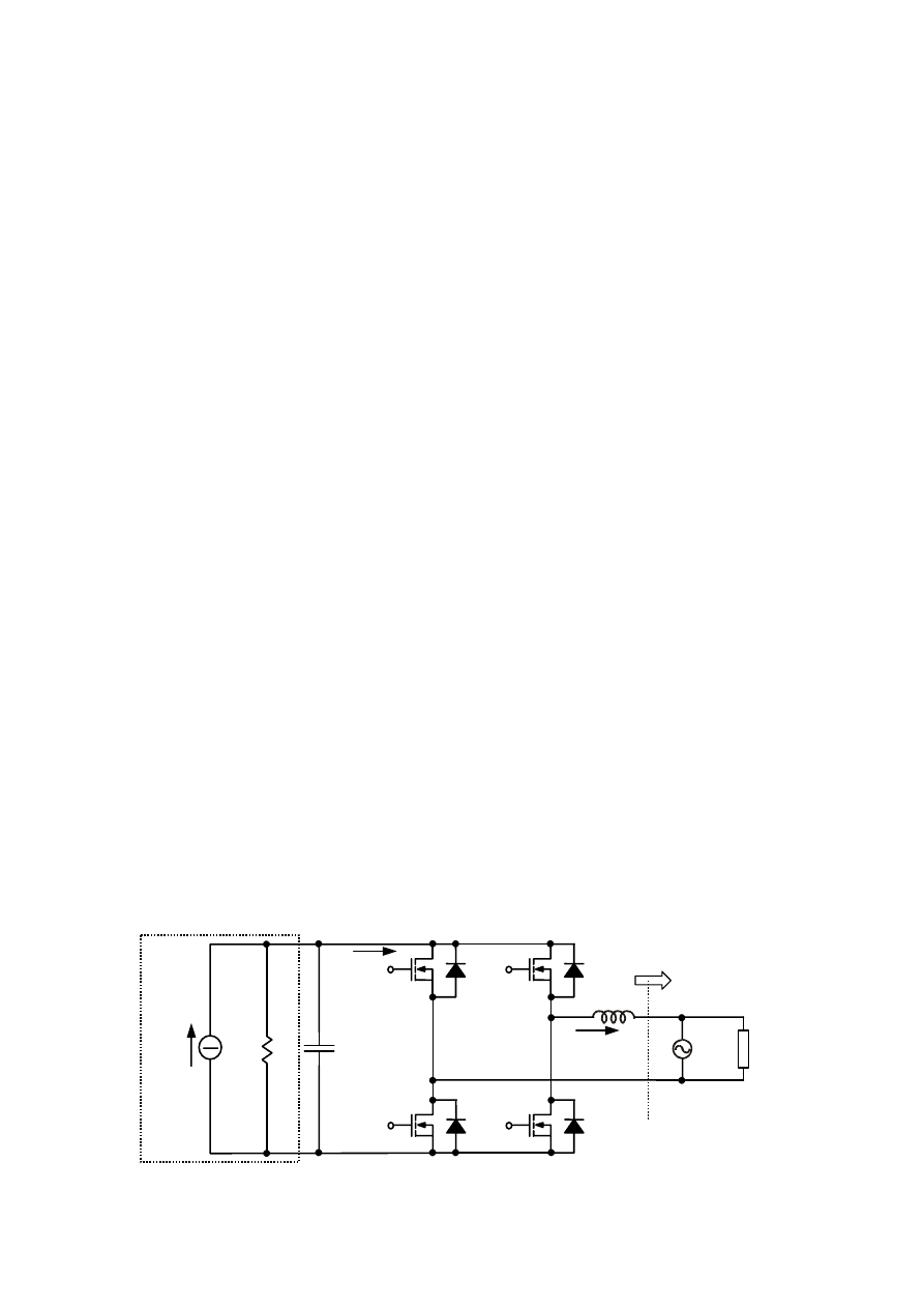
I
dc
L
u
g
i
L
load
p
out
u
o
+
-
i
in
+
U
dc
+
-
C
i
R
dc
DC source
model
Fig. 1 - Converter basic scheme.
a design procedure both for the converter passive
components and for the basic control parameters, defining
an optimal modulation strategy. Based on this, it is possible
to control the power flux to the utility grid in a wide range,
while maintaining the current displacement factor close to
unity.
A small signal dynamic model is also derived, suitable
for control stability analysis. Experimental results are given,
that validate the theoretical analysis and demonstrate the
feasibility of the approach.
II. C
ONVERTER
D
ESCRIPTION AND
B
ASIC
O
PERATION
The proposed single-phase inverter is shown in Fig. 1.
The converter supplies the load with power coming from a
dc source (fuel cell), which we represent with its Norton
equivalent. This allows us to account for the non negligible
output impedance of the cell i.e. to model its typical
voltage/current characteristic [5-7], at least in the so-called
ohmic polarization region. Parameter values can be directly
derived from the typical proton exchange membrane fuel
cell (PEMFC) characteristic (cell voltage / current density).
Considering, for example, a nominal output voltage of
200 V (at nominal output current) and a nominal power of
2.5
kW we determined I
dc
= 24 A, R
dc
= 16.7
Ω
. The
converter is actually fed by a dc voltage U
dc
, across
capacitor C
i
, which, given the non ideal characteristics of
the source, has to be suitably regulated. The dc source
operating point is controlled by adjusting the average input
current I
in
absorbed by the power converter so as to keep the
dc link voltage U
dc
at the desired level. In general, for a
correct converter operation, an input voltage close to the line
peak voltage may be required. As a consequence, the fuel
cell stack needs to be specifically designed or the series
connection of several commercial stacks may be considered.
The basic converter operation is as a controlled current
source. By forcing the fundamental component of current i
L
to be in phase with voltage u
g
= U
g
⋅
sin(
θ)
,
θ
=
ω
t, one can
minimize the current required to extract the nominal active
power from the dc source. The regulation of the active
power injected into the grid allows to vary the average input
current I
in
and so to control the input voltage and the cell
operating point. Since the grid determines the load voltage,
possible exceeding power coming from the dc source is
automatically injected into the utility. Similarly, reactive
power required by the load circulates through the grid and
does not affect the converter. As can be seen, no battery or
other significant energy tank is connected to the dc/ac
converter. Because of that, it is not possible to accept
significant variations of the regulated output power. These
would cause inefficient use of fuel and/or significant power
dissipation within the cell. As known, any fuel cell response
to modifications in the fuel flow presents typical time
constants between one to a few minutes. Consequently,
operation in the absence of the grid is not possible, unless an
energy storage device is included in the system. In case of a
grid fault, our system has to be disconnected.
III. C
ONVERTER
A
NALYSIS IN
CCM
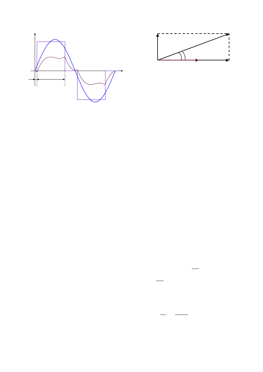
Assuming the converter operates in CCM, as with any
three level modulation strategy (e.g. phase shift
modulation), the converter main waveforms are shown in
Fig. 2. As can be seen, the inverter generates a three-level
voltage pulse with adjustable conduction angle
θ
c
and delay
angle
θ
d
with respect to the line voltage u
g
zero crossing.
According to our control strategy, we want the converter
output current i
L
to be in phase with the line voltage u
g
. We
also want to maintain the input voltage U
dc
at a given value,
which requires the control of the average input current I
in
.
Deriving the expression of the inverter voltage fundamental
harmonic component, as a function of control and converter
parameters, it is possible to find the conditions on angles
θ
c
and
θ
d
which need to be satisfied in order to get the desired
result. The situation is described by the vector diagram,
referring to the fundamental components, shown in Fig. 3.
Imposing the phase condition (i
L
in phase with u
g
), we
derived the constraint (1), which relates angles
θ
c
and
θ
d
.
( )
(
)
M
2
cos
cos
c
d
d
π
=
θ
+
θ
−
θ
, (1)
where
g
dc
U
U
M
=
.
Then, by imposing the output power to be equal to a
given amount P
g
, we derived constraint (2).
(
)
( )
gN
d
c
d
P
sin
sin
=
θ
−
θ
+
θ
, (2)
where
g
dc
g
g
N
g
gN
U
U
L
P
P
P
P
πω
=
=
is the normalized output
power delivered to the line.
θθθθ
2π
2π
2π
2π
u
g
(
θθθθ
)
i
L
(
θθθθ
)
u
o
(
θθθθ
)
θθθθ
d
θθθθ
c
0
Fig. 2 - Inverter output voltage and current waveforms together with
line voltage waveform in a line period (CCM).
g
U
&
1
L
U
&
1
o
U
&
ββββ
1
L
I&
Fig. 3 - Vector diagram of fundamental inductor voltage
U
&
L1
, line
voltage U
&
g
, inverter output voltage fundamental component U
&
o1
and inductor fundamental current
1
L
I&
, assuming only active power
delivered to the line.
Constraints (1) and (2) need to be simultaneously
satisfied, so we combined them to derive the expressions of
conduction angle
θ
c
and normalized output power, as
functions of the delay angle
θ
d
. The results are graphically
shown in Fig. 4 for the following converter parameters:
U
g
= 311V, f
g
= 50Hz, U
dc
= 290V, L = 10mH.
As can be seen in Fig. 4b, the maximum power is
transferred to the line for
θ
d
= 0. Substituting
θ
d
= 0 into (1)
and (2) we get:
(
)
2
max
c
max
gN
M
2
1
1
sin
P
π
−
−
=
θ
=
. (3)
Given the desired nominal output power, (3) imposes a
constraint on dc link voltage U
dc
and filter inductor value L.
Therefore, attention can be put both on device voltage stress
and output current harmonic content (the bigger L, the
smoother i
L
current). Equation (3) allows to calculate the
conduction angle
θ
cmax
, needed to transfer the required
nominal power. Using (1) and (2), it is finally possible to
calculate the maximum delay angle
θ
dmax
, shown in Fig. 4,
that corresponds to P
gN
= 0.
It is worth noting that the relation between output power
and delay angle is almost linear (Fig. 4b). We verified that
this "linearity" is maintained in a wide range of voltage
conversion ratios M. This property has been exploited to
determine a simple modulation law for the converter which,
based on a single control variable that directly controls the
output power, varies the delay and conduction angles
simultaneously so as to keep the fundamental component of
current i
L
in phase with u
g
. A similar approach is discussed
in more detail, in the next section, for the DCM operation.
We completed the analysis in CCM by calculating the
expression of the average current I
in
drawn by the inverter.
Current i
in
is instantaneously equal to the inverter output
current during the
θ
c
interval. The output current can be
calculated integrating the inductor voltage and imposing
CCM operation. Averaging the instantaneous input current
in a line period we get:
[
]
d
c
d
g
g
in
sin
)
(
sin
L
U
I
θ
−
θ
+
θ
πω
=
. (4)
It is worth noting that the average current, drawn by the
converter from the dc source, does not depend on the input
voltage value U
dc
. This implies that, in open loop conditions,
the voltage set-point only depends on the dc source
characteristics (I
dc
, R
dc
), and thus can vary significantly
during the operation, for example because of temperature
and/or gas pressure variations within the cell. We therefore
investigated also the converter's behavior in DCM.
IV. C
ONVERTER
A
NALYSIS IN
DCM
Modifying the switch control strategy as in Fig. 5, where
the switch gate signals are shown, it is possible to achieve a
discontinuous mode of operation. When the current in the
inductor L gets to zero, it is not allowed to invert because
three switches are off. With this strategy, depending on the
choice of L and U
dc
the converter can operate in DCM up to
the nominal power or only to a fraction of it.
As in the CCM case, we still want the current
fundamental component to be in phase with the output
voltage and the power extracted from the dc source to be
equal to the nominal value. In this case the analysis of the
ω
t
2
π
u
g
(
θθθθ
)
S
3
S
4
S
1
S
2
θ
c
θ
d
θ
c
θ
d
ω
t
ω
t
ω
t
ω
t
θ
x
i
L
(
θθθθ
)
u
o
(
θθθθ
)
Fig. 5- Modulation strategy for DCM operation
a)
1.9
2.1
2.2
2.3
2.4
0
0.1
0.2
0.3
0.4
0.5
2
θθθθ
dmax
θθθθ
cmax
θθθθ
d
[rad]
θθθθ
c
[rad]
b)
0
0.1
0.2
0.3
0.4
0.5
0
0.1
0.2
0.3
0.4
0.5
0.6
0.7
θθθθ
dmax
θθθθ
d
[rad]
P
gN
P
gNmax
Fig. 4 - a) relation between conduction angle
θ
c
and delay
angle
θ
d
. b) normalized output power as a function of
θ
d
.
voltage pulse fundamental harmonic component is more
complicated because the waveform is no longer rectangular
(Fig.
5). Therefore, the analytical expressions of the
constraints we derived for the control angles are quite
cumbersome and only their numerical solution is practical.
The key equations are given in the Appendix. The numerical
solution procedure generates Fig.
6, which shows, for
different U
dc
values, the relationship between angles
θ
d
and
θ
c
that has to be satisfied to get in-phase converter current
and line voltage. It is worth noting that, as in the CCM case,
also in DCM the phase condition does not depend on the
value of L. As can be seen in Fig. 6, differently from the
CCM case, for each U
dc
value there is a minimum delay
angle
θ
d
, below which the converter is not able to satisfy the
phase condition. This limit angle increases with U
dc
voltage,
so that Fig. 6 poses an upper limit to the U
dc
value.
Assuming that a modulation law can be implemented
which varies the angles
θ
d
and
θ
c
according to what is
shown in Fig. 6, we can easily compute the normalized
power P
gN
transferred to the line. This is shown in Fig. 7, as
a function of both angle
θ
c
and
θ
d
. As can be seen,
differently from the CCM case, the resulting relations are
both non-linear. As in the CCM case, the absolute maximum
power transferred to the line occurs at the minimum
θ
d
angle
and is inversely proportional to L and directly proportional
to U
dc
. A possible design procedure could consist again in
selecting the DC link voltage to get a sufficiently large
control angle range (according to Fig. 6) and to make a
proper choice of inductor L to get the required output power
level. In order to limit line current THD, the L value should
not be reduced too much. However [4] shows how this
limitation can be compensated by introducing a suitable
auxiliary commutation circuit.
The DCM analysis can be completed by calculating the
expression of the average converter input current I
in
.
Following the same procedure outlined for the CCM case,
we derived expression (5). As can be seen, I
in
now depends
on input voltage U
dc
.
(
)
[
]
2
c
dc
d
c
d
c
d
g
g
in
L
2
U
....
cos
sin
sin
L
U
I
θ
πω
+
+
θ
θ
−
θ
−
θ
+
θ
πω
=
(5)
In case of open loop operation, the "resistive" behavior
of the power converter, implied by the last addendum of (5),
helps to maintain the desired input voltage. We investigate
this issue by simulations, considering different values for the
I
dc
parameter, as a simplified model of possible operating
condition variations within the cell. For a
±
10% variation of
the I
dc
parameter, in CCM operation we found a
±
20%
variation of the U
dc
voltage, while, in DCM, for the same
output power, the U
dc
variation reduced to
±
6.5 %. This is
basically the reason why we decided to design the power
converter to operate in DCM up to the nominal power.
V. C
ONVERTER
C
ONTROL IN
DCM
Equation (5) can be easily linearized, by perturbation
around a given operating point, with respect to variations of
the U
dc
voltage and of the control variable
α
. Variable
α
represents the output of the controller that determines the
converter operating point, i.e. angles
θ
d
and
θ
c
. Of course, a
suitable modulation law must be implemented relating
α
and
the control angles
θ
d
and
θ
c
. As explained in the following,
we derived the modulation law so as to get an approximately
linear relation between variable
α
and the power delivered
to the line P
g
, because this greatly simplifies the design of
the controller.
The perturbation method allowed us to derive a small
signal linear dynamic model of the power converter, which
is of the type shown in the right part of Fig. 8. As can be
seen, our model basically consists of two current sources:
the Norton current source I
dc
with output resistance R
dc
representing the fuel cell and the current source I
in
representing the converter. The
∼
symbol indicates deviation
of a variable around the selected operating point value.
Parameters I
eq
and G
eq
, shown in Fig. 8 are defined in (6).
10
20
30
40
50
60
70
80 90
0
20
40
60
80
100
120
θθθθ
c
[deg]
θθθθ
d
[deg]
U
dc
= 170 V
U
dc
= 190 V
U
dc
= 210 V
U
dc
= 230 V
Fig. 6 - Relation between angles
θ
c
and
θ
d
to satisfy the phase
condition for different U
dc
values.
0.2
0.4
0.6
0.8
θθθθ
c
,
θθθθ
d
[deg]
P
gN
0
P
gN
(
θθθθ
d
)
0
10
20
30
40
50
60
70
80
90
P
gN
(
θθθθ
c
)
Fig. 7 - Normalized line power as a function of angles
θ
c
and
θ
d
U
dc
+
-
I
dc
I
in
C
i
+
-
G
eq
i
dc
∼
u
dc
∼
I
eq
⋅α
∼
C
i
R
dc
R
dc
Fig. 8 - Dynamic model of the converter: large signal (left) and small
signal (right)
(
)
(
)
(
)
( )
L
2
U
,
U
I
G
U
,
I
U
,
I
2
c
dc
dc
in
eq
dc
in
dc
eq
πω
α
θ
=
α
∂
∂
=
α
α
∂
∂
=
α
(6)
The exact expression for I
eq
is quite complicated, as it is
easy to see, because the control angles are both functions of
α
, through the modulation law. However, if the linearization
of the relation between
α
and the transferred power P
g
is
implemented, for any given U
dc
value the I
eq
value is
constant for the entire
α
range. This happens because also
the relation between I
in
and
α
in this case becomes linear.
Therefore, linearizing the relation between
α
and P
g
eliminates the problem of a variable small signal gain when
it comes to controlling the power converter, giving a
significant advantage in the controller design.
To derive the modulation law, satisfying the phase
condition and being simple enough to be easily
implemented, a suitable linear approximation of the
relations shown in Fig. 6 can be determined. Then, angles
θ
d
and
θ
c
can be generated as a function of a single variable,
which we call
γ
. A non linear function
f
which approximates
the inverse of the resulting relation between P
g
and
γ
can
then be determined and used to process the control variable,
before angles
θ
d
and
θ
c
are computed. We found that a
quadratic approximation is normally good enough to achieve
the desired linearization. Of course, this solution is viable
only in case of a digital implementation of the control
system, as in our case. We consequently developed the
modulator based on the following equations:
0
d
d
d
0
c
c
c
m
m
)
(
f
θ
+
γ
⋅
=
θ
θ
+
γ
⋅
=
θ
α
=
γ
, (7)
where
α
is the actual control variable (0<
α
<1) which now
linearly controls the normalized power transferred to the
line, f is the non linear function that linearizes the relation
between
α
and the transferred power, m
c
,
θ
c0
, m
d
,
θ
d0
are
control parameters, to be determined by approximating the
relation between
θ
d
and
θ
c
, depicted in Fig.
6, and
corresponding to the selected input voltage. Another
constraint can be imposed for the control angle
θ
c
. This can
be limited between 10° and 90° because below 10° there is
practically no power variation, while the maximum power is
reached when
θ
c
= 90° (Fig. 7).
VI. C
ONTROL
D
ESIGN
E
XAMPLE
In our example we assume U
g
= 160 V. Based on Fig. 6
and on reasonable switch ratings we chose U
dc
= 200 V. By
selecting L = 10 mH we got a maximum output power
P
gMAX
= 2230 W and, according to the previously outlined
procedure, we determined the following parameter values:
m
c
= 1.396, m
d
= -1.117,
θ
c0
= 0.175,
θ
d0
= 1.46. With these
values, the resulting relation between
γ
and the line power
P
g
is shown in Fig. 9. After function f was determined
approximating the inverse of the relation P
g
(
γ
), we obtained
the relation between the control variable
α
and P
g
, also
shown in Fig. 9. As can be seen, a good linearity is
achieved.
Based on the linear model in Fig. 8, a controller can be
found that allows to regulate the input voltage U
dc
and to
extract the desired active power from the source. Given the
first order structure of the system, a suitable choice can be a
PI regulator, which is possible to design locating the
regulator's zero at the system's pole frequency and then
fixing the integral gain k
I
so as to get the desired crossover
frequency
ω
cr
, according to (8).
eq
cr
dc
eq
I
dc
eq
I
P
I
)
R
/
1
G
(
k
R
/
1
G
C
k
k
ω
⋅
+
=
+
=
(8)
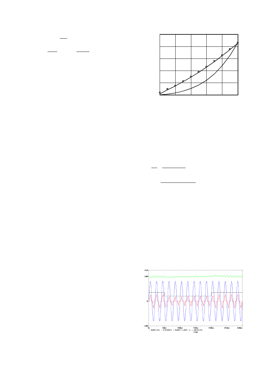
In order to verify the results of this analysis, Pspice
simulation of the system was performed. Initially we
verified the correctness of the modulation law by evaluating,
for different
α
values, the resulting transferred power and
comparing it with the analytical result of Fig. 9. The results
are shown as dots in Fig. 9.
We successively verified the open loop and closed loop
performance of the system. In open loop conditions we
verified that our model is capable of predicting with good
accuracy both voltage variation and settling time in response
to a step variation of I
dc
. In closed loop conditions we
checked the performance of the PI controller we designed
according to the given procedure. A typical response to step
variations of the I
dc
current is shown in Fig. 10.
0
0.2
0.4
0.6
0.8
1
0
500
1000
1500
2000
2500
P
g
[W]
γ,α
γ,α
γ,α
γ,α
P
g
(
γγγγ
)
P
g
(
α
αα
α
)
Fig. 9 - Line power as a function of control variables
γ
and
α
,
computed for U
g
= 160 V, U
dc
= 200 V, L = 10 mH. Dots represent
simulation results.
Fig. 10 - Simulated converter operation with PI control. From top to
bottom: regulated U
dc
voltage, line voltage, input current (X10) and
line current (X2).
VII. E
XPERIMENTAL
R
ESULTS
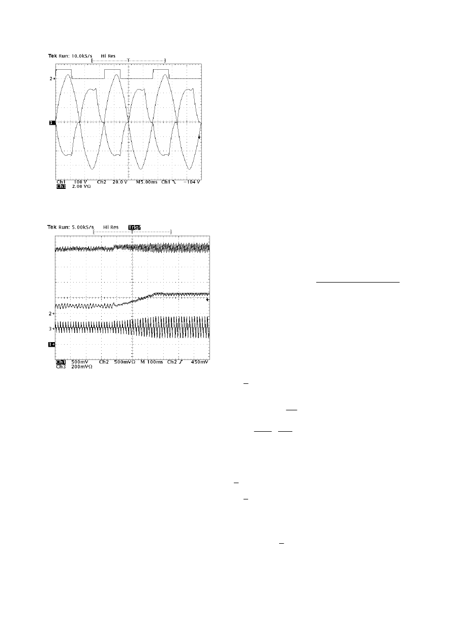
A first prototype of the converter, designed for a reduced
output power of 800 W, is currently under test. The dc
supply is a laboratory power supply. We show in Fig. 11 an
example of operation in DCM. The line voltage is 220 V
RMS
,
the circuit injects 740 W into the grid. The PF is 0.985.
Fig. 12 shows instead the dynamic performance of the
control system. A linear variation of I
dc
current (middle
trace) determines a U
dc
voltage rise (top trace) which is
compensated by the control system by increasing the
injected line current (bottom trace).
VIII. C
ONCLUSIONS
This paper analyses a single phase, low frequency
commutated VSI usable as a rugged and low-cost interface
between a renewable dc source and the utility grid. The
target application is represented by low to medium power
fuel cells used in co-generation systems. Switching at the
line frequency, the converter presents negligible switching
losses and EMI generation. Moreover, the simplicity of the
required control circuitry makes it particularly robust and
inexpensive. The paper includes the detailed analysis of the
converter in CCM and DCM. The analysis allows to outline
a design procedure both for the converter passive
components and for the basic control parameters, defining
an optimal modulation strategy. Experimental results are
also given, that validate the theoretical analysis and
demonstrate the feasibility of the approach.
R
EFERENCES
[1] - G. A. O´Sullivan, “Fuel Cell Inverter for Utility Applications”, CD-
ROM of the IEEE Power Electronics Specialists Conference,
Galway, Ireland, June 2000.
[2] - U.S. Department of Energy et al., “2001 Future Energy Challenge”,
Homepage URL: HYPERLINK
http://energy.uiuc.edu/energychallenge/main.html/FutureEnergyCha
llenge
[3] - G. Ledwich and P. Wang, “Simple Grid Interfaces for Renewables”,
International Journal of Renewable Energy Engineering, vol. 1, No.
2, August 1999, pp. 50-55.
[4] - G. M. Martins, J. A. Pomilio, S. Buso, "A Single-Phase Low-
frequency Commutation Inverter for Renewables", IECON'01 Conf.
Proc., Denver, USA, November 2001, pp. 1976-1981.
[5]
-
M.A. Brown, T.L. Pryor, P. Singh, "Comparison of Diesel
Generator, Proton Exchange Membrane Fuel Cell and Alkaline Fuel
Cell System Efficiencies for the Production of AC Power in Remote
Area Power Supply Applications", International Journal of
Renewable Energy Engineering, Vol. 3, No. 2, August 2001,
pp.297-304.
[6] - K. Kordesch, G. Simader, Fuel Cell and Their Applications, VCH
Verlagsgesellschaft mbH, 1996.
[7] - E. Santi, D. Franzoni, A. Monti, D. Patterson, F. Ponci, N. Barry,
"A Fuel Cell Based Domestic Uninterruptible Power Supply",
APEC 2002 Conf. Proc., Dallas, USA, March 2002, pp. 605-613.
A
PPENDIX
In DCM the condition determining in phase line current and voltage is
given by:
[
]
(
)
[
]
π
⋅
=
θ
−
θ
⋅
+
+
θ
−
θ
⋅
+
π
⋅
+
θ
+
θ
−
θ
k
)
2
sin(
)
2
sin(
2
k
...
...
k
k
)
cos(
)
cos(
d
x
x
d
c
d
d
(A1)
where (see also Fig. 5)
( )
θ
⋅
−
θ
=
θ
c
g
dc
d
x
U
U
cos
cos
a
(A2)
and
M
2
1
U
2
U
k
dc
g
⋅
=
⋅
=
. It is worth noting that (A1) is a generalization of
(1), where the second addendum is determined by the different voltage
pulse waveform typical of DCM, which presents also sinusoidal
components i.e. it is no longer a three level voltage pulse. Equation (A1)
can be simplified and re-written as follows:
[
]
[
]
0
)
2
sin(
)
2
sin(
2
1
...
...
)
cos(
)
cos(
k
1
d
x
x
d
c
d
d
=
θ
−
θ
⋅
+
+
θ
−
θ
+
θ
+
θ
−
θ
⋅
. (A3)
The power transferred to the line is instead given by:
(
)
( )
[
]
( )
( )
(
)
θ
−
θ
⋅
−
+
+
θ
−
θ
+
θ
=
x
d
d
c
d
gN
2
cos
2
cos
2
k
...
...
sin
sin
P
, (A4)
which can be interpreted again as a generalization of (2), where the second
addendum is due to the sinusoidal components of the inverter voltage pulse.
Fig. 11- Converter operation at reduced power. From top to bottom:
S
2
command, input voltage [100V/div], line current [2A/div].
U
dc
I
dc
i
L
Fig. 12 - Dynamic behavior of the controller. From to to bottom:
voltage U
dc
(10 V/div), current I
dc
(2A/div), line current i
L
(5A/div).
Wyszukiwarka
Podobne podstrony:
Control of a single phase three level voltage source inverter for grid connected photovoltaic system
A Composite Pwm Method Of Three Phase Voltage Source Inverter For High Power Applications
A Simplified Functional Simulation Model for Three Phase Voltage Source Inverter Using Switching Fun
A Composite Pwm Method Of Three Phase Voltage Source Inverter For High Power Applications
MODELLING GRID CONNECTED VOLTAGE SOURCE INVERTER OPERATION
A Series Active Power Filter Based on a Sinusoidal Current Controlled Voltage Source Inverter
A Series Active Power Filter Based on Sinusoidal Current Controlled Voltage Source Inverter
Algebraic PWM Strategies of a Five Level NYC Voltage Source Inverter
Algebraic PWM Strategies of a Five Level NYC Voltage Source Inverter
A Series Active Power Filter Based on Sinusoidal Current Controlled Voltage Source Inverter
An Active Power Filter Implemented With A Three Level Npc Voltage Source Inverter
A New Medium Voltage PWM Inverter Topology for Adjustable Speed Drives
Design of a 10 kW Inverter for a Fuel Cell
Simulation for Fuel Cell Inverter using Simplorer and Simulink
więcej podobnych podstron