
GUIDE TO UNDERSTANDING JTAG
FUSES AND SECURITY
A N I N TE R M E DI ATE LO O K AT TH E AV R J TA G I N TE R FA CE
AVRFREAKS.NET
SEP 2002

AN INTERMEDIATE LOOK AT THE AVR JTAG INTERFACE, AVRFREAKS.NET
1
TABLE OF CONTENTS
Understanding JTAG fuses and Security .............................................................................................2
JTAG Nomenclature...............................................................................................................................2
JTAG Fuses and Security......................................................................................................................2
On-Chip Debugging ...............................................................................................................................3
Boundary-Scan.......................................................................................................................................4
JTAG Programming ...............................................................................................................................5
JTAG Security Roundup ........................................................................................................................5
JTAG Programming ...............................................................................................................................6

AN INTERMEDIATE LOOK AT THE AVR JTAG INTERFACE, AVRFREAKS.NET
2
Understanding JTAG fuses and Security
We will in this article take a closer look at the JTAG interface and how Fuses and
Lockbits affect operation. If you are using, or planning to use the JTAG interface,
you should definitely spend a couple of minutes reading this article!
Note: This article is not intended for newbies. Readers should read and get an
understanding of the JTAG section in the datasheet before reading this document.
Introduction
New megaAVR devices with more than 8KB of Flash, include a JTAG interface for
Programming, Boundary Scan and On-chip Debugging.
This article will take a peek at some of the features that are somewhat hidden, or
difficult to find, in the datasheets.
JTAG Nomenclature
JTAG Programming, OCD, IEEE 1149.1 compliant, Boundary-Scan. It is easy to
get confused and start mixing the terminology. To summarize the AVR JTAG
interface is compliant with the IEEE 1149.1 Standard. Through this interface you
have access to the following "services":
•
Memory Programming
•
Boundary Scan
•
On-Chip Debug
When using the term "JTAG" we refer to the interface as such. When talking
about a specific "service" we usually use the "service name". (e.g. JTAG
Programming)
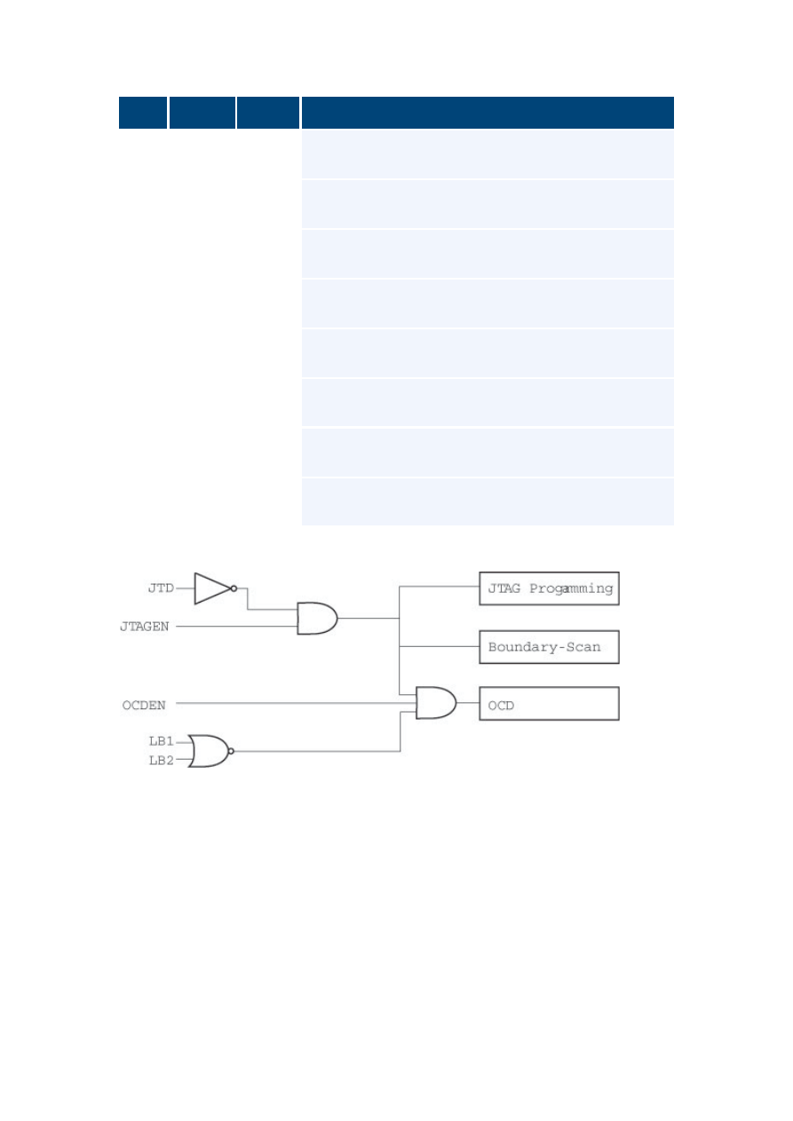
JTAG Fuses and Security
JTAG
Fuses
The first source of confusion when looking at the JTAG interface is understanding
the fuses, and how they affect the behavior of the device and/or JTAG interface.
In addition; An IO control bit "JTD" is a available. Unlike the fuses this bit can be
set at run-time allowing you to disable the JTAG / OCD functionality in software
during program execution.
So what is the difference between the JTAGEN and OCDEN fuse? What do they
do, and what is the consequence of only programming one of them?
To save you some time fine-reading the Datasheet, we here at AVRfreaks have
compiled the following table and functional block diagram that should explain the
relationship between these fuses and functionality.
The block diagram below the table shows the relationship between the Fuses and
JTD control bit. Note that setting either of the Lock bits LB1or LB2 will disable
OCD.
NOTE: In the following table we use "P" for programmed, and "U" for un-
programmed fuse.
AN INTERMEDIATE LOOK AT THE AVR JTAG INTERFACE, AVRFREAKS.NET
3
JTD
JTAGEN
OCDEN
DESCRIPTION
U
U
U
No JTAG programming, OCD or Boundary-Scan is
possible
U
U
P
No JTAG programming, OCD or Boundary-Scan is
possible
U
P
U
JTAG Programming and Boundary Scan is possible,
OCD disabled
U
P
P
OCD, JTAG Programming and Boundary-Scan is
Enabled (Note 1)
P
U
U
No JTAG programming, OCD or Boundary-Scan is
possible
P
U
P
No JTAG programming, OCD or Boundary-Scan is
possible
P
P
U
No JTAG programming, OCD or Boundary-Scan is
possible
P
P
P
No JTAG programming, OCD or Boundary-Scan is
possible
Note 1: Do not ship the device in this state, as it will consume more power, and
is open for hacking :-)
JTAG
Security
As shown in the figure and table, setting the correct fuses and keeping the device
unlocked is essential to be able to access the on-chip OCD system. As shown,
setting lock bits will disable the OCD system completely, while the JTAG
Programming interface will continue to work the same way as the two other
programming interfaces (HVPP and ISP).
To disable JTAG Programming, either set appropriate Lock bits, or use the JTD bit
or the JTAGEN fuse.
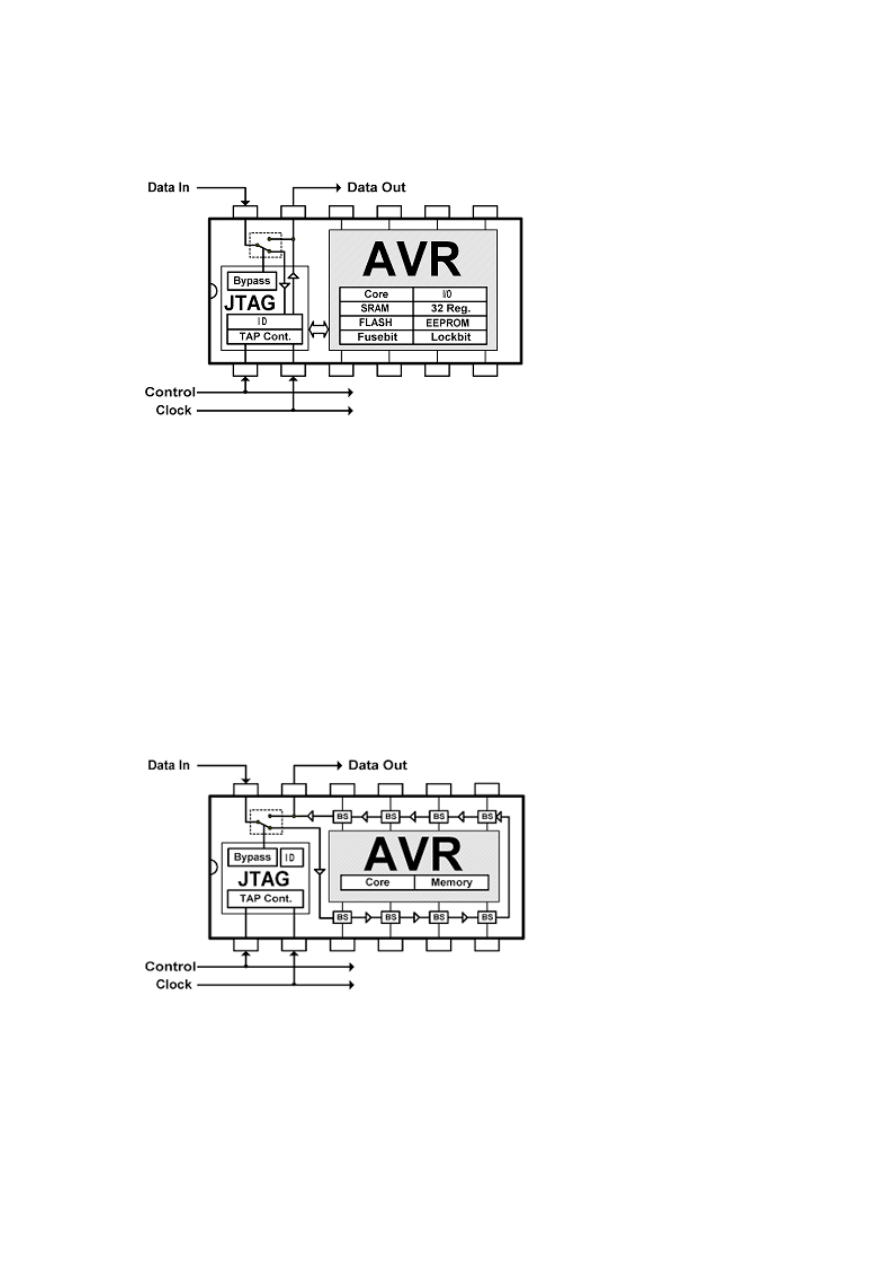
On-Chip Debugging
The OCD is a feature for in-system debugging. Although this "emulation" interface
lack some of the functionality offered by high end emulators (features like
trace/triggers unlimited breakpoints, cycle counters...) it actually has some
AN INTERMEDIATE LOOK AT THE AVR JTAG INTERFACE, AVRFREAKS.NET
4
unique features not found in any other emulator: The most obvious advantage is
that you actually are running the code on the device itself, so all electrical and
timing characteristics are FOR REAL. No emulated behavior!
The main thing to remember is that the JTAG OCD is not an EMULATOR, it is the
real thing. Which leads us to the JTAG ICE which actually is no ICE at all. It is a
protocol converter/interface allowing AVR Studio to talk to the OCD interface
inside the AVR. :-)
One thing that you should be aware of is that when the AVR OCDEN fuse is
programmed (OCD Enabled) some of the clock system is left running even though
you put the AVR in sleep mode. So, if you experience high power consumption
during SLEEP mode, make sure you are not running the device with the OCDEN
programmed!
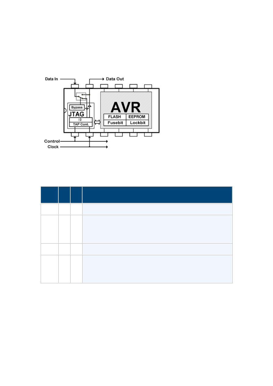
Boundary-Scan
Boundary-Scan is very efficient way of verifying that your device is soldered in
correctly, and that inter connectivity to other devices is correct. There are a
number of tools available today that will read your layout files and generate a
complete test vector set to verify your design.
When JTAGEN fuse is programmed and JTD is not set, the Boundary Scan Chain
is available. This chain include all (almost) physical pins on the device. This chain
do not include the internal scan chain. The internal Scan Chain is part of the OCD
system, and is not accessible unless OCD is enabled, and LB1 and LB2 is
unprogrammed.
AN INTERMEDIATE LOOK AT THE AVR JTAG INTERFACE, AVRFREAKS.NET
5
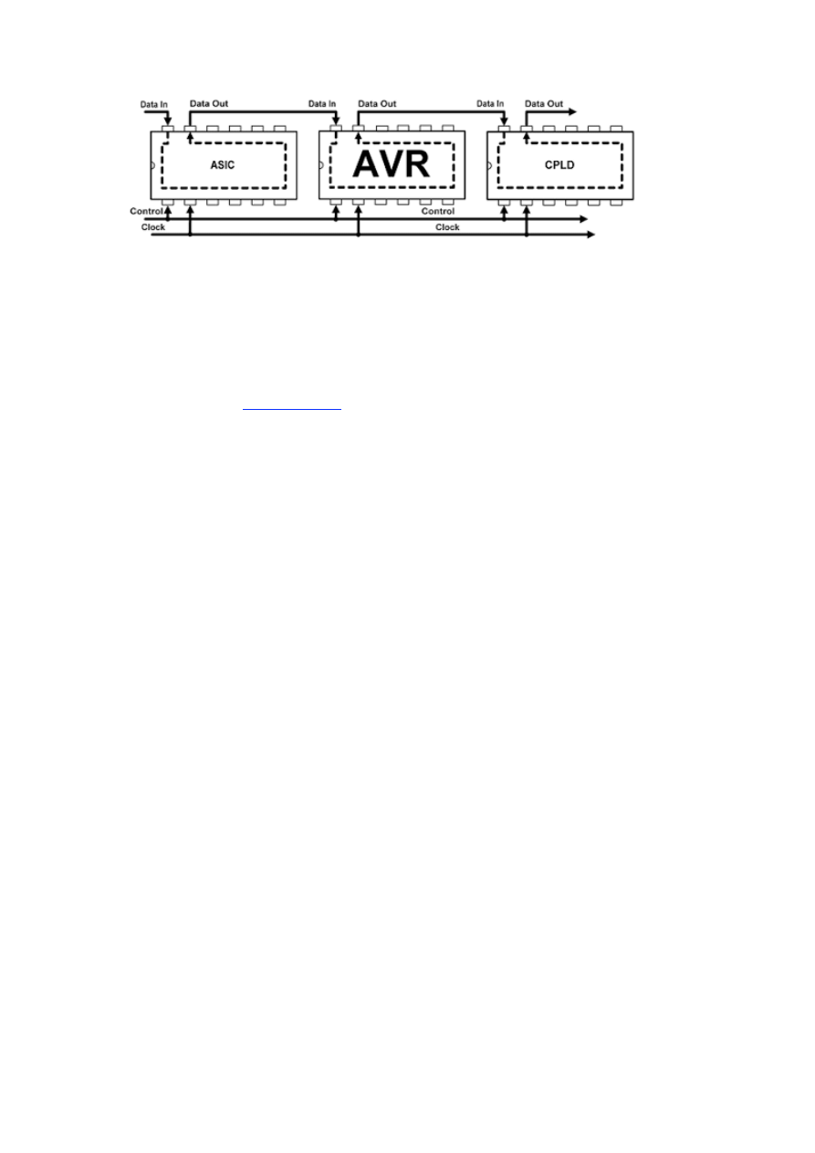
JTAG Programming
The JTAG programming interface works much the same way as the two other
programming interfaces. The same functionality and restrictions apply. The main
thing to remember if you want to use the JTAG for programming is to set the
Lock bits correctly. Setting the JTAGEN will not do you any good if you have
disabled Further write or Read/write by programming the Lock Bits!
This table explains the relationship between JTAG Programming interface and the
Lock Bits:
NOTE: In the following table we use "P" for programmed, and "U" for un-
programmed fuse.
LB
mode
LB2
LB1
DESCRIPTION
1
U
U
No memory lock features enabled.
2
U
P
Further programming of the Flash and EEPROM is disabled in
Parallel and SPI/JTAG Serial Programming mode. The Fuse bits
are locked in both Serial and Parallel Programming mode. Read-
back is possible.
-
P
U
Invalid Mode
3
P
P
Further programming and verification of the Flash and EEPROM
is disabled in Parallel and SPI/JTAG Serial Programming mode.
The Fuse bits are locked in both Serial and Parallel
Programming mode.
JTAG Security Roundup
We have now looked at the different services offered by the JTAG interface, and
the final task is to take an analysis of the security of the JTAG implementation.
AN INTERMEDIATE LOOK AT THE AVR JTAG INTERFACE, AVRFREAKS.NET
6
Let's take a feature by feature approach.
JTAG Programming
The JTAG Programming interface is controlled by the same lock bits controlling all
other programming interfaces. So it will be as secure as any of them.
On-Chip Debug
As Shown in the
block diagram
the only way to enabled OCD is to leave the lock
bits off and then enabling both JTAGEN and OCDEN. In this state, the device is
totally open anyway so the easiest way to steal code from it is to use any ISP
programmer and dump out the code directly. With lock bits programmed, the
OCD is disables ( regardless of LB mode ). So here the OCD is even more secure
than the standard ISP interface where you can read out the memory contents in
both LB mode 1 and 2.
Boundary Scan
This one is interesting, what if we could use the boundary scan chain to grab out
info that we are not supposed to get hold of?! Luckily (unfortunately; depending
who you are..), this is not possible. The Boundary Scan chain do not include any
internal signal, only physical package pins. If the internal scan chain was
accessible from the Boundary Scan interface, it would be possible to grab out the
program counter and instruction word, thus stealing the contents of the flash
array bypassing the lock bits! Luckily (for most..) this is not possible. The internal
scan chain is part of the OCD interface, and thus only accessible when no
memory lock bits are programmed.
Conclusion
Our conclusion is that the JTAG interface is safe. But as with all security features
they require that they are activated to have any effect :-)
Wyszukiwarka
Podobne podstrony:
Cambridge University Press A Guide to MATLAB for Beginners and Experienced Users J5MINFIO6YPPDR6C36
Nuelow Guide to Being Trampled, Stomped and Mangled
Guide to the Gods A fuller and more detailed list of Asatru heathen deities
A Short Guide to Occult Symbols Pentacles and Pentagrams NA4W0302
The Agile Manager s Guide to Understandi by Joseph T Straub
Using Malware to Improve Software Quality and Security
NIST Technical Guide to Information Security Testing and Assessment SP800 115
Herbs for Sports Performance, Energy and Recovery Guide to Optimal Sports Nutrition
Guide to the properties and uses of detergents in biology and biochemistry
A Guide to the Law and Courts in the Empire
Jouni Yrjola Easy Guide to the Classical Sicilian (feat Richter Rauzer and Sozin Attacks)
PRICING INTELLIGENCE 2 0 A Brief Guide to Price Intelligence and Dynamic Pricing by Mihir Kittur
Penguin Readers Teacher's Guide to using Film and TV
Asperger's Disorder A Medical Dictionary, Bibliography, And Annotated Research Guide To Internet Ref
Money and Happiness A Guide to Living the Good Life
Guide To Budgets And Financial Management
A KABBALISTIC GUIDE TO LUCID DREAMING AND ASTRAL PROJECTION
więcej podobnych podstron