2N3055
SILICON NPN TRANSISTOR
■
SGS-THOMSON PREFERRED SALESTYPE
■
NPN TRANSISTOR
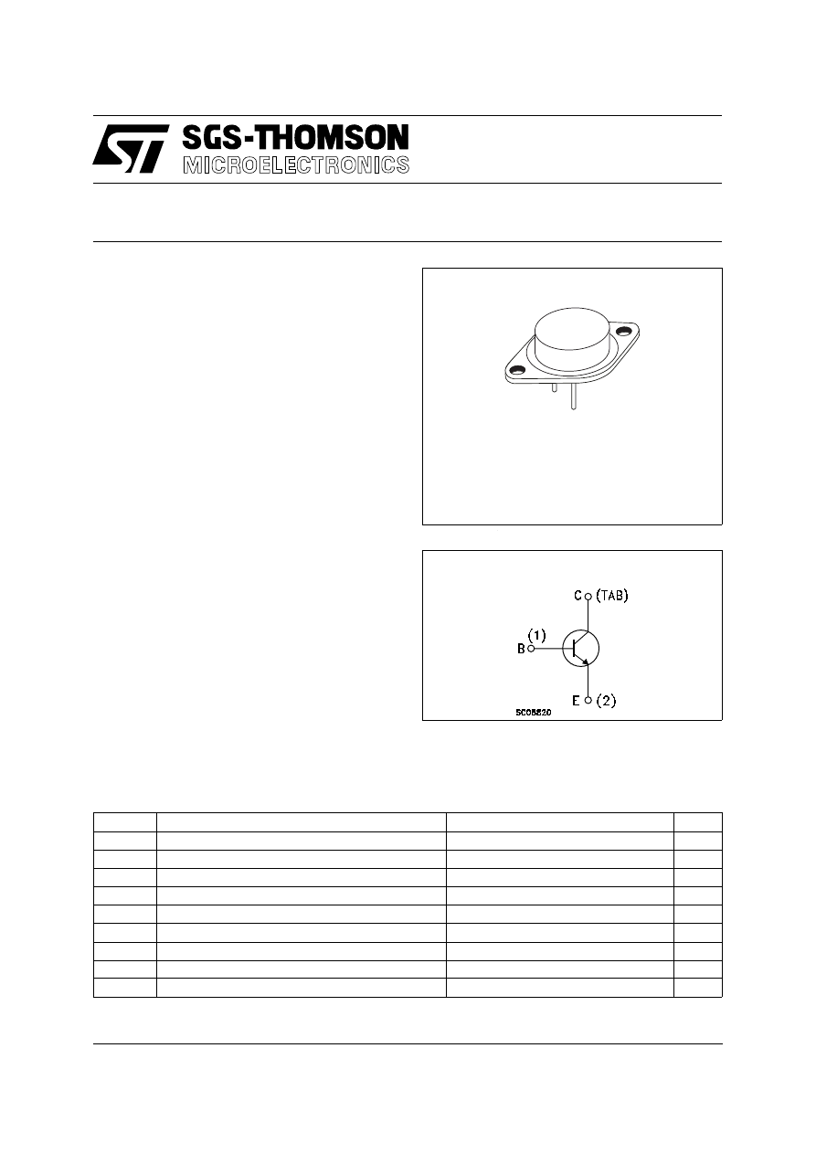
DESCRIPTION
The 2N3055 is a silicon epitaxial-base NPN
transistor in Jedec TO-3 metal case. It is intended
for power switching circuits, series and shunt
regulators, output stages and high fidelity
amplifiers.
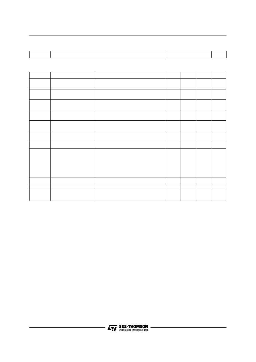
INTERNAL SCHEMATIC DIAGRAM
June 1997
ABSOLUTE MAXIMUM RATINGS
Symbol
Parameter
Value
Unit
V
CBO
Collector-Base Voltage (I
E
= 0)
100
V
V
CER
Collector-Emitter Voltage (R
BE
= 100
Ω
)
70
V
V
CEO
Collector-Emitter Voltage (I
B
= 0)
60
V
V
EBO
Emitter-Base Voltage (I
C
= 0)
7
V
I
C
Collector Current
15
A
I
B
Base Current
7
A
P
tot
Total Dissipation at T
c
≤
25
o
C
115
W
T
stg
Storage Temperature
-65 to 200
o
C
T
j
Max. Operating Junction Temperature
200
o
C
1
2
TO-3
1/4
THERMAL DATA
R
thj-case
Thermal Resistance Junction-case Max
1.5
o
C/W
ELECTRICAL CHARACTERISTICS (T
case
= 25
o
C unless otherwise specified)
Symbol
Parameter
Test Conditions
Min.
Typ.
Max.
Unit
I
CEV
Collector Cut-off
Current (V
BE
= -1.5V)
V
CE
= 100 V
V
CE
= 100 V T
j
= 150
o
C
1
5
mA
mA
I
CEO
Collector Cut-off
Current (I
B
= 0)
V
CE
= 30 V
0.7
mA
I
EBO
Emitter Cut-off Current
(I
C
= 0)
V
EB
= 7 V
5
mA
V
CEO(sus)
∗
Collector-Emitter
Sustaining Voltage
I
C
= 200 mA
60
V
V
CER(sus)
∗
Collector-Emitter
Sustaining Voltage
I
C
= 200 mA R
BE
= 100
Ω
70
V
V
CE(sat)
∗
Collector-Emitter
Saturation Voltage
I
C
= 4 A I
B
= 400 mA
I
C
= 10 A I
B
= 3.3 A
1
3
V
V
V
BE
∗
Base-Emitter Voltage
I
C
= 4 A V
CE
= 4 V
1.5
V
h
FE
∗
DC Current Gain
I
C
= 0.5 A V
CE
= 4 V Group 4
I
C
= 0.5 A V
CE
= 4 V Group 5
I
C
= 0.5 A V
CE
= 4 V Group 6
I
C
= 0.5 A V
CE
= 4 V Group 7
I
C
= 4 A V
CE
= 4 V
I
C
= 10 A V
CE
= 4 V
20
35
60
120
20
5
50
75
145
250
70
h
FE1
/
h
FE1
∗
DC Current Gain
I
C
= 0.5 A V
CE
= 4 V
1.6
f
T
Transition frequency
I
C
= 1 A V
CE
= 4 V
2.5
MHz
I
s/b
∗
Second Breakdown
Collector Current
V
CE
= 40 V
2.87
A
∗
Pulsed: Pulse duration = 300
µ
s, duty cycle 1.5 %
2N3055
2/4
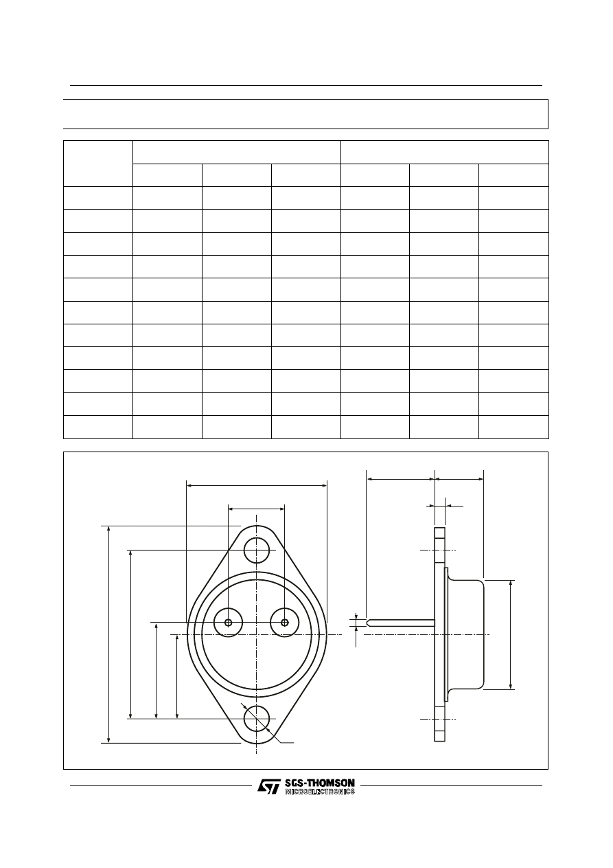
DIM.
mm
inch
MIN.
TYP.
MAX.
MIN.
TYP.
MAX.
A
11.00
13.10
0.433
0.516
B
0.97
1.15
0.038
0.045
C
1.50
1.65
0.059
0.065
D
8.32
8.92
0.327
0.351
E
19.00
20.00
0.748
0.787
G
10.70
11.10
0.421
0.437
N
16.50
17.20
0.649
0.677
P
25.00
26.00
0.984
1.023
R
4.00
4.09
0.157
0.161
U
38.50
39.30
1.515
1.547
V
30.00
30.30
1.187
1.193
E
B
R
C
D
A
P
G
N
V
U
O
P003F
TO-3 MECHANICAL DATA
2N3055
3/4

Information furnished is believed to be accurate and reliable. However, SGS-THOMSON Microelectronics assumes no responsability for the
consequences of use of such information nor for any infringement of patents or other rights of third parties which may results from its use. No
license is granted by implication or otherwise under any patent or patent rights of SGS-THOMSON Microelectronics. Specifications mentioned
in this publication are subject to change without notice. This publication supersedes and replaces all information previously supplied.
SGS-THOMSON Microelectronics products are not authorized for use as critical components in life support devices or systems without express
written approval of SGS-THOMSON Microelectonics.
© 1997 SGS-THOMSON Microelectronics - Printed in Italy - All Rights Reserved
SGS-THOMSON Microelectronics GROUP OF COMPANIES
Australia - Brazil - Canada - China - France - Germany - Hong Kong - Italy - Japan - Korea - Malaysia - Malta - Morocco - The Netherlands -
Singapore - Spain - Sweden - Switzerland - Taiwan - Thailand - United Kingdom - U.S.A
. . .
2N3055
4/4
Wyszukiwarka
Podobne podstrony:
2N3055, MJ2955 (STMicroelectronics)
2N3055 id 32663 Nieznany (2)
2N3055 MJ2955
2N3055 id 32663 Nieznany (2)
TDA7388 STMicroelectronics elenota pl
TDA7383 STMicroelectronics elenota pl
TDA7566 STMicroelectronics elenota pl
L6506 (STMicroelectronics)
TDA7266M STMicroelectronics elenota pl
SGSPx16, SGSPx17 (STMicroelectronics)
TDA7850 STMicroelectronics elenota pl
VIPery nowa rodzina zintegrowanych kontrolerów STMicroelectronics do zasilaczy
TDA7490LSA STMicroelectronics elenota pl
TDA1908 STMicroelectronics elenota pl (1)
BUZ11 (STMicroelectronics)
TDA7233 STMicroelectronics elenota pl
więcej podobnych podstron