
F2833x - Interrupts
6 - 1
Introduction
This module is used to explain the interrupt system of the F2833x Digital Signal Controller.
So what is an interrupt?
Before we go into the technical terms, let us start with an analogy: Think of a nice evening and
you are working at your desk, preparing the laboratory experiments for the next day. Suddenly
the phone rings, you answer it and then you get back to work (after the interruption). The shorter
the phone call, the better! Of course, if the call comes from your girlfriend you might have to re-
think your next step due to the “priority” of the interruption… Anyway, sooner or later you will
have to get back to the preparation of the task for the next day; otherwise you might not pass the
next exam.
This analogy touches some basic definitions for interrupts;
•
interrupts appear “suddenly”: in technical terms, this is called “asynchronous”
•
interrupts might be more or less important: they have a “priority”
•
they must be dealt with before the phone stops ringing: “immediately”
•
the laboratory preparation should be continued after the call - the “interrupted task is
resumed”
•
the time spent with the phone call should be as small as possible - “interrupt latency”
•
after the call, you should continue your work from the exact place where you left it -
“context save” and “context restore”
To summarize the technical terms:
Interrupts are defined as asynchronous events, generated by an external or internal hardware unit.
An event causes the controller to interrupt the execution of the current program and to start a
service routine, which is dedicated to this event. After the execution of this interrupt service
routine, the program that was interrupted will be resumed.
The quicker a CPU performs this “task-switch”, the more this controller is suited for real-time
control. After going through this chapter, you will be able to understand the F2833x interrupt
system.
At the end of this chapter, we will perform an exercise with a program controlled by interrupts
that uses one of the 3 core timers of the CPU. The core timer’s period interrupt will be used to
perform a periodic task.
Interrupt System

Module Topics
6 - 2
F2833x - Interrupts
Module Topics
Interrupt System ........................................................................................................................................6-1
Introduction .............................................................................................................................................6-1
Module Topics ..........................................................................................................................................6-2
F2833x Core Interrupt Lines ...................................................................................................................6-3
The F2833x RESET ..................................................................................................................................6-4
Reset Bootloader ......................................................................................................................................6-5
Interrupt Sources .....................................................................................................................................6-9
Maskable Interrupt Processing ..............................................................................................................6-10
Peripheral Interrupt Expansion .............................................................................................................6-12
Hardware Interrupt Response ................................................................................................................6-15
F2833x CPU Timers ..............................................................................................................................6-16
Summary: ...............................................................................................................................................6-18
Lab 6: CPU Timer 0 Interrupt and 4 LEDs ...........................................................................................6-19
Objective............................................................................................................................................6-19
Procedure ...........................................................................................................................................6-19
Create a Project File ..........................................................................................................................6-19
Project Build Options ........................................................................................................................6-20
Modify the Source Code ....................................................................................................................6-20
Build, Load and Test .........................................................................................................................6-21
Modify Source Code - Part 2 .............................................................................................................6-21
Build, Load and Test .........................................................................................................................6-24

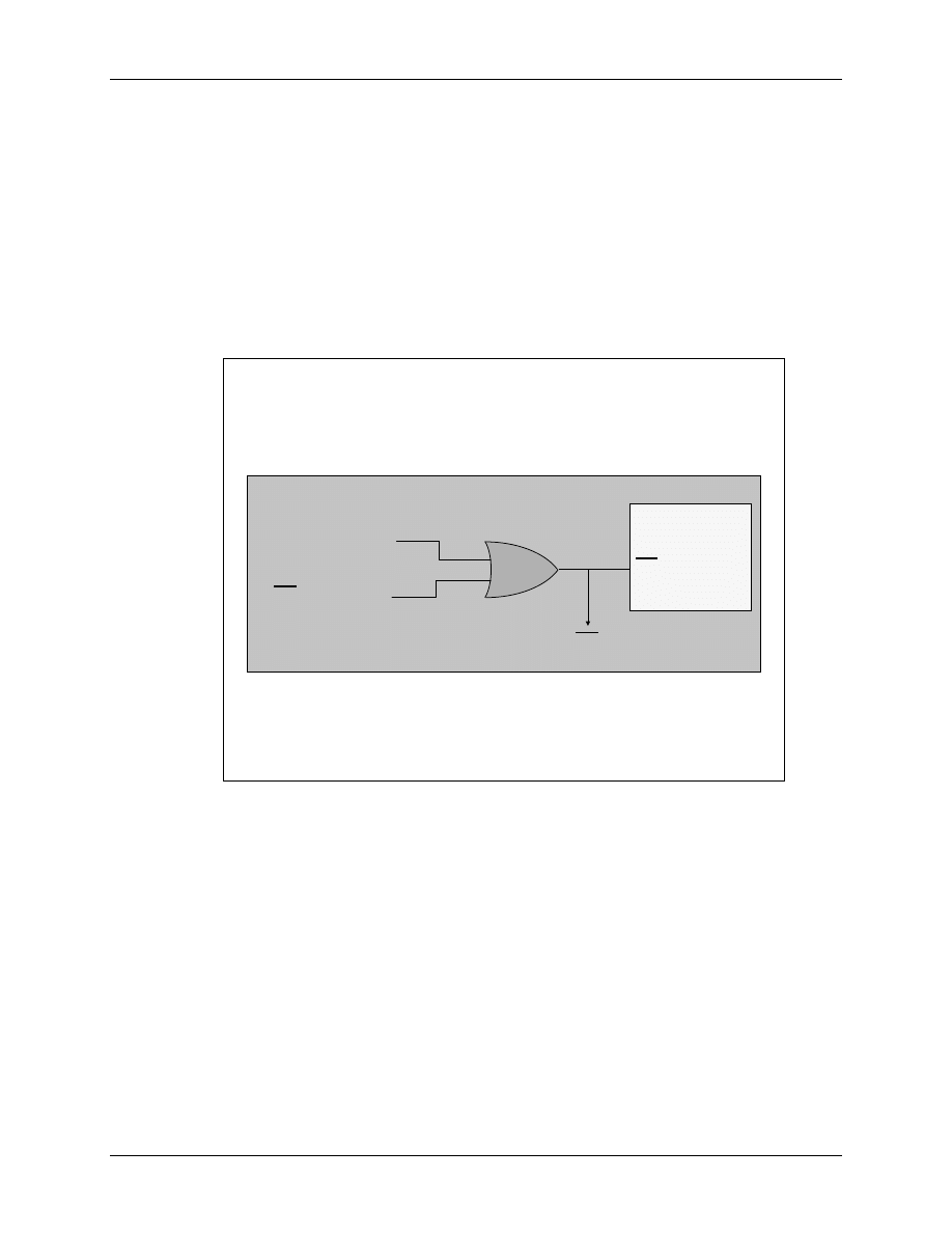
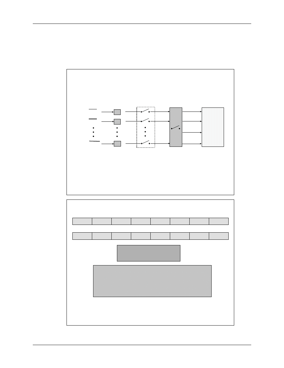
F2833x Core Interrupt Lines
F2833x - Interrupts
6 - 3
F2833x Core Interrupt Lines
The core interrupt system of the F2833x consists of 16 interrupt lines; two of them are called
“Non-Maskable” (RESET, NMI). The other 14 lines are ‘maskable’ - this means the programmer
can allow or disable interrupts from these 14 lines.
What does the phrase “mask” stand for?
A “mask” is a binary combination of ‘1’ and ‘0’. A ‘1’ stands for an enabled interrupt line, a ‘0’
for a disabled one. By loading the mask into register “IER” we can select, which interrupt lines
will be enabled to request an interrupt service from the CPU.
For a “non-maskable” interrupt, we cannot disable an interrupt request. Once the signal line goes
active, the running program will be suspended and the dedicated interrupt service routine will
start. Generally, “non-maskable” interrupts are used for high priority and safety based events e.g.
emergency stop.
6
6
-
-
2
2
F2833x Core Interrupt Lines
F2833x Core Interrupt Lines
F2833x
F2833x
CORE
CORE
2 non
2 non
-
-
maskable
maskable
interrupts (RS,
interrupts (RS,
“
“
selectable
selectable
”
”
NMI)
NMI)
14 maskable interrupts
14 maskable interrupts
(INT1
(INT1
–
–
INT14)
INT14)
INT1
INT1
INT2
INT2
INT3
INT3
INT4
INT4
INT5
INT5
INT6
INT6
INT7
INT7
INT8
INT8
INT9
INT9
INT10
INT10
INT11
INT11
INT12
INT12
INT13
INT13
INT14
INT14
RS
RS
NMI
NMI
All 16 lines are connected to a table of ‘interrupt vectors’, which consists of 32 bit memory
locations per interrupt. It is the responsibility of the programmer to fill this table with the start
addresses of dedicated interrupt service routines. However, in case of the F2833x, this table is in
ROM and filled with addresses, defined by Texas Instruments in such a way, that /RS points to
address 0x00 0040, NMI to address 0x00 0042 an so on. All these addresses are in RAM, so the
programmer has to fit a single 32-bit instruction into these memory locations.
The F2833x RESET
6 - 4
F2833x - Interrupts
The F2833x RESET
A high to low transition at the external “/RS” pin will cause a reset of the Digital Signal
Controller. The next rising edge of /RS will force the CPU to read the code start address from
address 0x3F FFC0 in code memory. This event is not an ‘interrupt’ in the sense that the old
program will be resumed. A reset is generated during powering up the device.
Another source for a reset is the overflow of the watchdog timer. To inform all other external
devices that the CPU has acknowledged a reset, the device itself drives the reset pin active low.
This means that the reset pin must be bi-directional!
6
6
-
-
3
3
F2833x Reset Sources
F2833x Reset Sources
Watchdog Timer
Watchdog Timer
RS pin active
RS pin active
To RS pin
To RS pin
RS
RS
F2833x Core
F2833x Core
Reset will force the controller not only to start from address 0x3F FFC0, but it will also clear all
internal operation registers, reset a group of CPU-Flags to initial states and disable all 16 interrupt
lines. We will not go into details about all the flags and registers for now, please refer to the data
sheet for the F2833x.
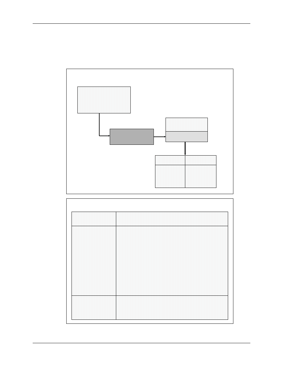
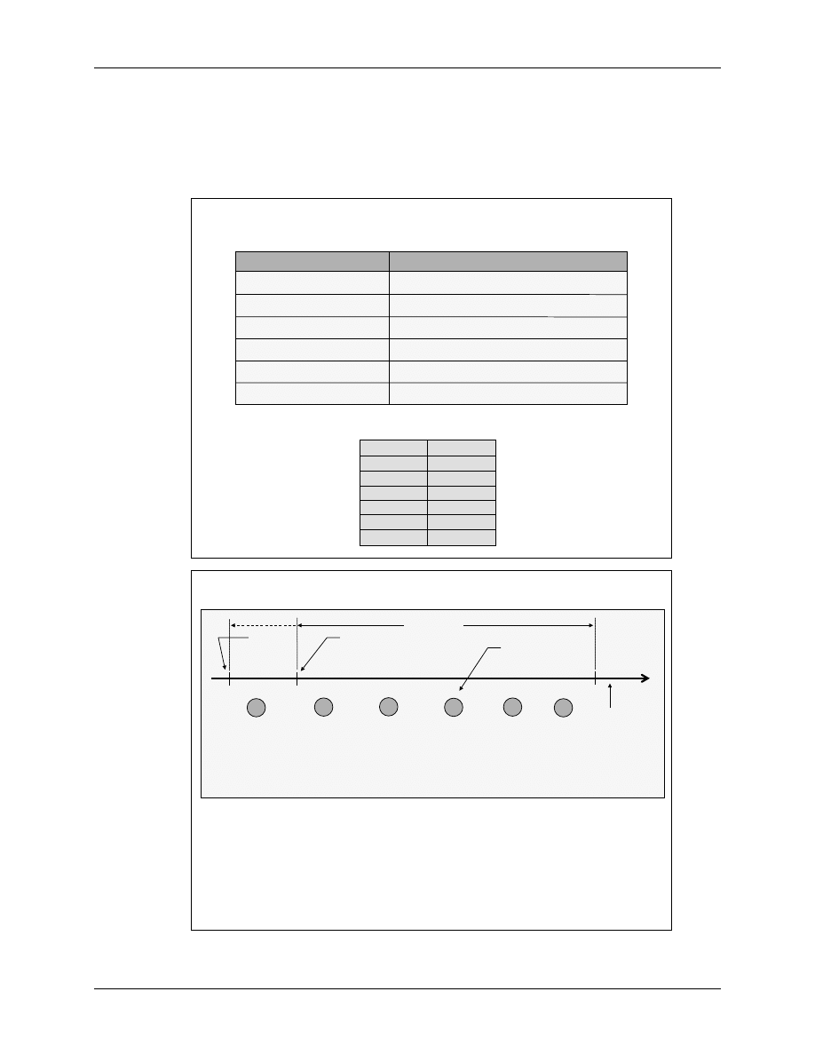
Reset Bootloader
F2833x - Interrupts
6 - 5
Reset Bootloader
After a RESET signal has been released, the CPU starts the execution of a first code section in
ROM, called “boot loader”. This function determines the next step, depending on the status of
four GPIO -pins (GPIO87, 86, 85 and 84).
6
6
-
-
4
4
Reset
Reset
–
–
Bootloader
Bootloader
Reset
Reset
OBJMODE = 0 AMODE = 0
OBJMODE = 0 AMODE = 0
ENPIE = 0 INTM = 1
ENPIE = 0 INTM = 1
Boot determined by
Boot determined by
state of GPIO pins
state of GPIO pins
Reset vector fetched
Reset vector fetched
from boot ROM
from boot ROM
0x3F FFC0
0x3F FFC0
Execution
Execution
Bootloading
Bootloading
Entry Point
Entry Point
Routines
Routines
FLASH SCI
FLASH SCI
-
-
A / SPI
A / SPI
-
-
A
A
M0 SARAM
M0 SARAM
I2C
I2C
OTP
OTP
eCAN
eCAN
-
-
A
A
XINTF
XINTF
McBSP
McBSP
-
-
A
A
GPIO / XINTF
GPIO / XINTF
Bootloader
Bootloader
sets
sets
OBJMODE = 1
OBJMODE = 1
AMODE = 0
AMODE = 0
6
6
-
-
5
5
Bootloader
Bootloader
Options
Options
1 1 1 1 jump to
1 1 1 1 jump to
FLASH
FLASH
address 0x33 FFF6
address 0x33 FFF6
1 1 1 0
1 1 1 0
bootload
bootload
code to on
code to on
-
-
chip memory via
chip memory via
SCI
SCI
-
-
A
A
1 1 0 1
1 1 0 1
bootload
bootload
external EEPROM to on
external EEPROM to on
-
-
chip memory via
chip memory via
SPI
SPI
-
-
A
A
1 1 0 0
1 1 0 0
bootload
bootload
external EEPROM to on
external EEPROM to on
-
-
chip memory via
chip memory via
I2C
I2C
1 0 1 1 Call
1 0 1 1 Call
CAN_Boot
CAN_Boot
to load from
to load from
eCAN
eCAN
-
-
A
A
mailbox 1
mailbox 1
1 0 1 0
1 0 1 0
bootload
bootload
code to on
code to on
-
-
chip memory via
chip memory via
McBSP
McBSP
-
-
A
A
1 0 0 1 jump to
1 0 0 1 jump to
XINTF
XINTF
Zone 6 address 0x10 0000 for 16
Zone 6 address 0x10 0000 for 16
-
-
bit data
bit data
1 0 0 0 jump to
1 0 0 0 jump to
XINTF
XINTF
Zone 6 address 0x10 0000 for 32
Zone 6 address 0x10 0000 for 32
-
-
bit data
bit data
0 1 1 1 jump to
0 1 1 1 jump to
OTP
OTP
address 0x38 0400
address 0x38 0400
0 1 1 0
0 1 1 0
bootload
bootload
code to on
code to on
-
-
chip memory via
chip memory via
GPIO port A
GPIO port A
(parallel)
(parallel)
0 1 0 1
0 1 0 1
bootload
bootload
code to on
code to on
-
-
chip memory via
chip memory via
XINTF
XINTF
(parallel)
(parallel)
0 1 0 0 jump to
0 1 0 0 jump to
M0 SARAM
M0 SARAM
address 0x00 0000
address 0x00 0000
0 0 1 1 branch to check boot mode
0 0 1 0 branch to Flash without ADC calibration (TI debug only)
0 0 0 1 branch to M0 SARAM without ADC calibration (TI debug only)
0 0 0 0 branch to SCI-A without ADC calibration (TI debug only)
87 /
87 /
XA15
XA15
86 /
86 /
XA14
XA14
85 /
85 /
XA13
XA13
84 /
84 /
XA12
XA12
GPIO pins
GPIO pins
Reset Bootloader
6 - 6
F2833x - Interrupts
The F28335ControlCard pulls all four GPIO - input lines to ‘1’, so by default the start option
“jump to FLASH address 0x3F FFF6” is selected. This will force the controller to continue the
code sequence in FLASH memory. However, we do not currently have anything programmed
into FLASH memory. So why did all of our previous labs work? The answer is: we over-ruled the
hardware - sequence and forced the DSC into our own code entry point by using three of Code
Composer Studio Debug commands:
•
Reset CPU
-
force the DSC to Reset Address 0x3F FFC0
•
Restart
-
force the DSC directly to code entry point “c_int00”,
bypassing the hardware start sequence
•
Go Main
-
finish the “c_int00”, call “main()” and stop at the first
instruction of “main()”.
With the help of jumper J18 (SCI - Boot) on the Peripheral Explorer Board, we could change the
hardware sequence. If this jumper is closed, GPIO84 will be ‘0’ and the start sequence would go
to “boot load code to on-chip memory via SCI-A”. In this operation mode, the chip would wait
for a serial communication stream from a host, which is of no use for us for now. This mode will
be used in chapter 15.
The next flowchart summarises the reset code flow for all start options of the F2833x.
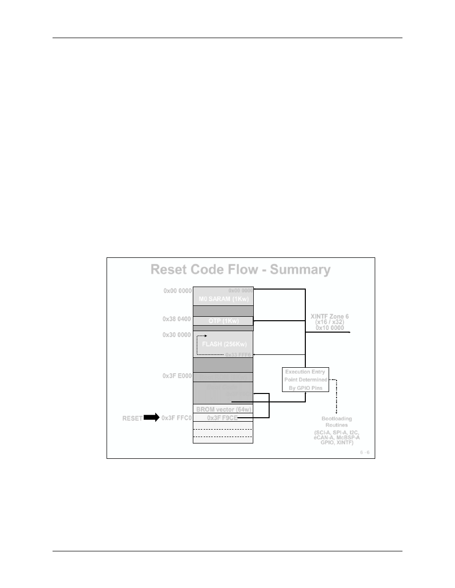
6 - 6
Reset Code Flow - Summary
M0 SARAM (1Kw)
FLASH (256Kw)
OTP (1Kw)
0x33 FFF6
0x38 0400
0x30 0000
0x00 0000
0x3F E000
0x3F FFC0
Boot ROM (8Kw)
BROM vector (64w)
0x3F F9CE
Boot Code
•
•
•
•
RESET
Execution Entry
Point Determined
By GPIO Pins
Bootloading
Routines
(SCI-A, SPI-A, I2C,
eCAN-A, McBSP-A
GPIO, XINTF)
0x3F F9CE
XINTF Zone 6
(x16 / x32)
0x10 0000
0x00 0000
The option ‘Flash Entry’ is usually used at the end of a project development phase when the
software flow is bug free. To load a program into the flash you will need to use a specific
program, available either as Code Composer Studio plug in or as a stand-alone tool. For our
current lab exercises we will refrain from loading (or ‘burning’) the flash memory.

Reset Bootloader
F2833x - Interrupts
6 - 7
The boot loader options via serial interface (SPI / SCI / I2C / eCAN / McBSP) or parallel port
(GPIO / XINTF) are usually used to download the executable code from an external host or to
update the contents of the flash memory. For these modes, please refer to chapters 15 and 16.
OTP-memory is a ‘one time programmable’ memory; there is no second chance to fit code into
this non-volatile memory. This option is usually used for company specific startup procedures
only. Again, to program this portion of memory you would need to use a Code Composer Studio
plug in. You might assess your experimental code to be worth storing forever, but for sure your
teacher will not. So, PLEASE do not upset your supervisor by using this option, he want to use
the boards for future classes!
The next two slides show the status of important core registers and status bits after a reset.
6
6
-
-
7
7
Register Bits Initialized at Reset
Register Bits Initialized at Reset
Register bits defined by reset
Register bits defined by reset
PC
PC
0x3F FFC0
0x3F FFC0
PC loaded with reset vector
PC loaded with reset vector
ACC
ACC
0x0000 0000
0x0000 0000
Accumulator cleared
Accumulator cleared
XAR0
XAR0
-
-
XAR7
XAR7
0x0000 0000
0x0000 0000
Auxiliary Registers
Auxiliary Registers
DP
DP
0x0000
0x0000
Data Page pointer points to page 0
Data Page pointer points to page 0
P
P
0x0000 0000
0x0000 0000
P register cleared
P register cleared
XT
XT
0x0000 0000
0x0000 0000
XT register cleared
XT register cleared
SP
SP
0x0400
0x0400
Stack Pointer to address 0400
Stack Pointer to address 0400
RPC
RPC
0x00 0000
0x00 0000
Return Program Counter cleared
Return Program Counter cleared
IFR
IFR
0x0000
0x0000
no pending interrupts
no pending interrupts
IER
IER
0x0000
0x0000
maskable interrupts disabled
maskable interrupts disabled
DBGIER
DBGIER
0x0000
0x0000
debug interrupts disabled
debug interrupts disabled
All internal math registers (ACC, P, XT) and auxiliary registers (XAR0 to XAR7) are cleared,
interrupts are disabled (IER) and pending interrupts, which have been requested before RESET,
are cancelled (IFR). The stack pointer (SP) is initialized to address 0x400 and the program
counter (PC) points to hardware start address 0x3F FFC0.

Reset Bootloader
6 - 8
F2833x - Interrupts
The two registers ST0 and ST1 combine all control and status flags of the CPU. Slide 6-8
explains the reset status of all the bits. ST0 contains all math bits such as zero (Z), carry (C) and
negative (N), whereas ST1 covers some more general operating mode bits.
We will postpone the discussion of the individual meaning of the bits until later chapters.
6
6
-
-
8
8
Control Bits Initialized at Reset
Control Bits Initialized at Reset
Status Register 0 (ST0)
Status Register 0 (ST0)
SXM = 0
SXM = 0
Sign extension off
Sign extension off
OVM = 0
OVM = 0
Overflow mode off
Overflow mode off
TC = 0
TC = 0
test/control flag
test/control flag
C = 0
C = 0
carry bit
carry bit
Z = 0
Z = 0
zero flag
zero flag
Status Register 1 (ST1)
Status Register 1 (ST1)
INTM = 1
INTM = 1
Disable all maskable interrupts
Disable all maskable interrupts
-
-
global
global
DBGM = 1
DBGM = 1
Emulation access/events disabled
Emulation access/events disabled
PAGE0 = 0
PAGE0 = 0
Stack addressing mode enabled/Direct addressing disabled
Stack addressing mode enabled/Direct addressing disabled
VMAP = 1
VMAP = 1
Interrupt vectors mapped to PM 0x3F FFC0
Interrupt vectors mapped to PM 0x3F FFC0
–
–
0x3F FFFF
0x3F FFFF
SPA = 0
SPA = 0
stack pointer even address alignment status bit
stack pointer even address alignment status bit
LOOP = 0
LOOP = 0
Loop instruction status bit
Loop instruction status bit
EALLOW = 0
EALLOW = 0
emulation access enable bit
emulation access enable bit
IDLESTAT = 0
IDLESTAT = 0
Idle instruction status bit
Idle instruction status bit
AMODE = 0
AMODE = 0
C27x/C28x addressing mode
C27x/C28x addressing mode
OBJMODE = 0
OBJMODE = 0
C27x object mode
C27x object mode
M0M1MAP = 1
M0M1MAP = 1
mapping mode bit
mapping mode bit
XF = 0
XF = 0
XF status bit
XF status bit
ARP = 0
ARP = 0
ARP points to AR0
ARP points to AR0
N = 0
N = 0
negative flag
negative flag
V = 0
V = 0
overflow bit
overflow bit
PM = 000
PM = 000
set to left
set to left
-
-
shift
shift
-
-
by
by
-
-
1
1
OVC = 00 0000
OVC = 00 0000
overflow counter
overflow counter
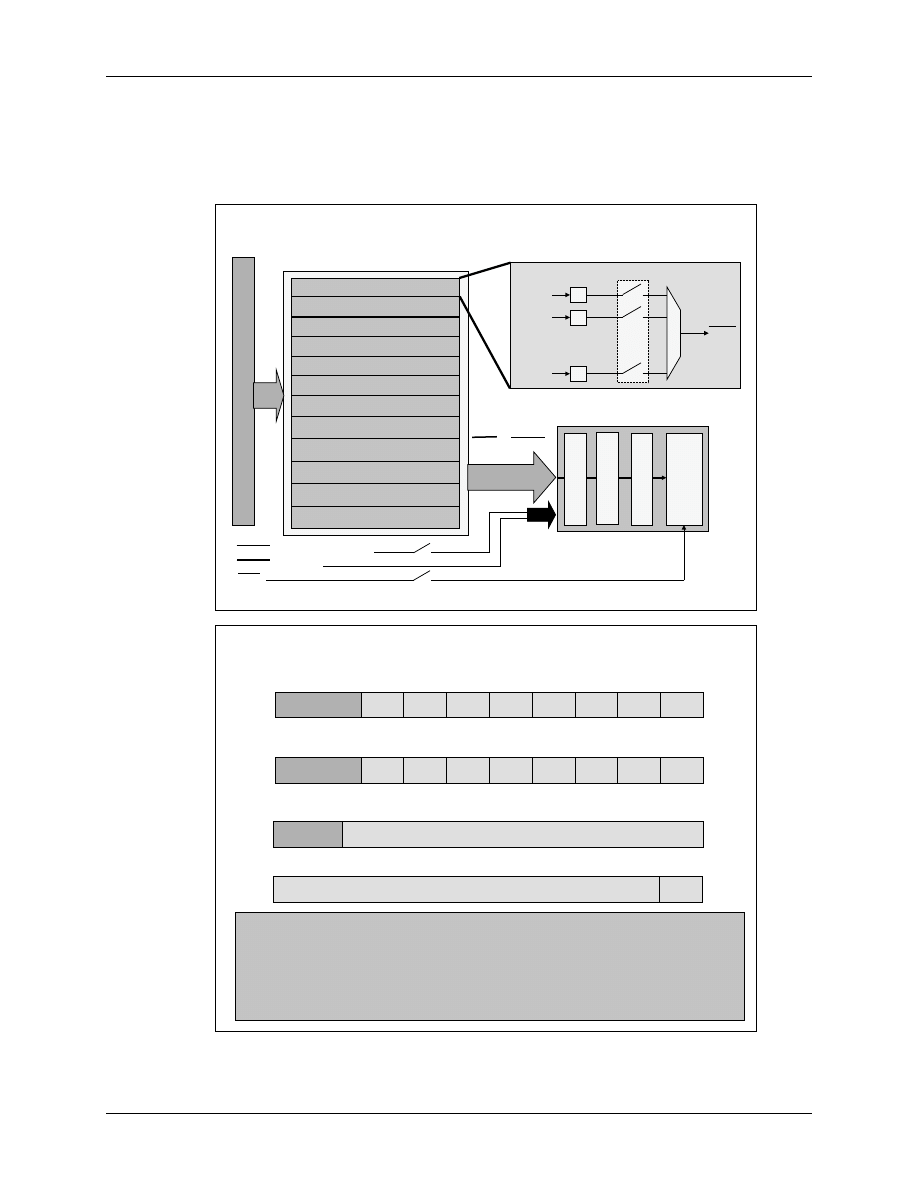
Interrupt Sources
F2833x - Interrupts
6 - 9
Interrupt Sources
As you can see from the next slide the DSP has a large number of interrupt sources (96 at the
moment) but only 14 maskable interrupt inputs. The question is: How do we handle this
‘bottleneck’?
Obviously we have to use a single INT-line for multiple sources. Each interrupt line is connected
to its interrupt vector, a 32-bit memory space inside the vector table. This memory space holds
the address for the interrupt service routine. In case of multiple interrupts this service routine
must be used for all incoming interrupt requests. This technique forces the programmer to use a
software based separation method on entry of this service routine. This method will cost
additional time that is often not available in real time applications. So how can we speed up this
interrupt service?
6
6
-
-
9
9
Interrupt Sources
Interrupt Sources
ePWM, eCAP,
ePWM, eCAP,
eQEP
eQEP
, ADC, SCI,
, ADC, SCI,
SPI, I2C, eCAN,
SPI, I2C, eCAN,
McBSP, DMA, WD
McBSP, DMA, WD
Internal Sources
Internal Sources
External Sources
External Sources
XINT1
XINT1
–
–
XINT7
XINT7
TZx
TZx
XRS
XRS
XNMI_XINT13
XNMI_XINT13
NMI
NMI
F2833x CORE
F2833x CORE
INT1
INT1
INT13
INT13
INT2
INT2
INT3
INT3
INT12
INT12
INT14
INT14
XRS
XRS
•
•
•
•
•
•
PIE
PIE
(Peripheral
(Peripheral
Interrupt
Interrupt
Expansion)
Expansion)
TINT2
TINT2
TINT1
TINT1
TINT0
TINT0
The answer from Texas Instruments is sweet, they simply used a pie. PIE stands for Peripheral
Interrupt Expansion unit.
This unit ‘expands’ the vector address table into a larger scale, reserving individual 32 bit entries
for each of the 96 possible interrupt sources. An interrupt response with the help of this unit is
much faster than without it. To use the PIE we will have to re-map the location of the interrupt
vector table to address 0x 00 0D00. This is in volatile memory! Before we can use this memory
we will have to initialise it.
Do not worry about the PIE-procedure for the moment, we will exercise all this during Lab6.
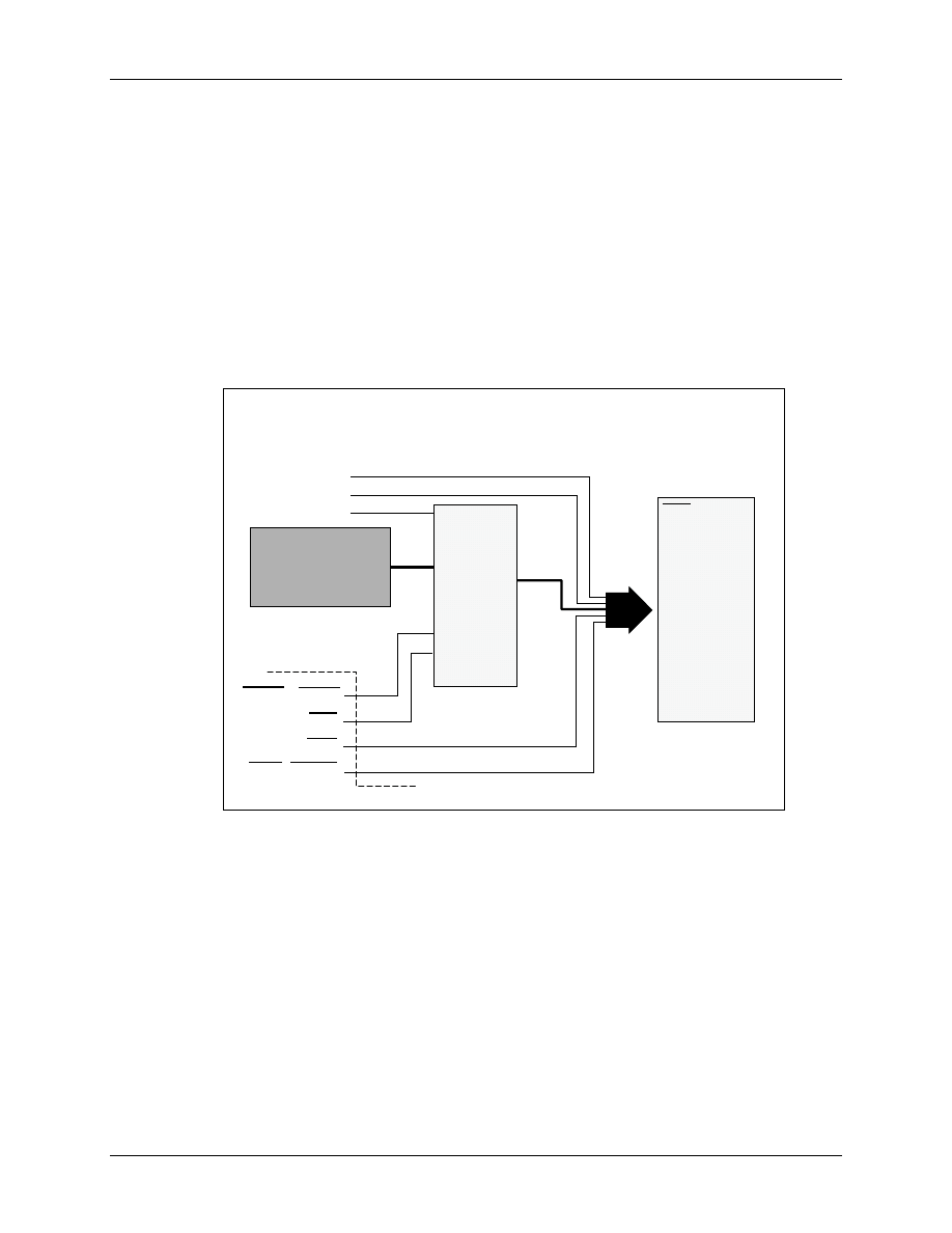
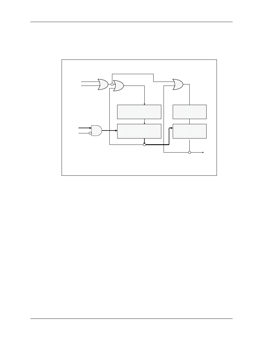
Maskable Interrupt Processing
6 - 10
F2833x - Interrupts
Maskable Interrupt Processing
Before we dive into the PIE-registers, we have to discuss the remaining path from an interrupt
request to its acknowledgement by the DSC. As you can see from the next slide, we have to close
two more switches to allow an interrupt request.
6
6
-
-
10
10
A valid signal on a specific interrupt line causes the latch
A valid signal on a specific interrupt line causes the latch
to display a
to display a
“
“
1
1
”
”
in the appropriate bit
in the appropriate bit
Maskable Interrupt Processing
Maskable Interrupt Processing
Conceptual Core Overview
Conceptual Core Overview
1
1
0
0
1
1
(
(
IFR
IFR
)
)
“
“
Latch
Latch
”
”
INT1
INT1
INT2
INT2
INT14
INT14
Core
Core
Interrupt
Interrupt
F2833x
F2833x
Core
Core
(
(
INTM
INTM
)
)
“
“
Global Switch
Global Switch
”
”
(
(
IER
IER
)
)
“
“
Switch
Switch
”
”
If the individual and global switches are turned
If the individual and global switches are turned
“
“
on
on
”
”
the
the
interrupt reaches the core
interrupt reaches the core
6
6
-
-
11
11
Interrupt Flag Register (IFR)
Interrupt Flag Register (IFR)
RTOSINT
RTOSINT
DLOGINT
DLOGINT
INT14
INT14
INT13
INT13
INT12
INT12
INT11
INT11
INT10
INT10
INT9
INT9
8
8
9
9
10
10
11
11
12
12
13
13
14
14
15
15
INT8
INT8
INT7
INT7
INT6
INT6
INT5
INT5
INT4
INT4
INT3
INT3
INT2
INT2
INT1
INT1
0
0
1
1
2
2
3
3
4
4
5
5
6
6
7
7
Pending :
Pending :
IFR
IFR
Bit
Bit
= 1
= 1
Absent :
Absent :
IFR
IFR
Bit
Bit
= 0
= 0
Compiler generates atomic instructions (non
Compiler generates atomic instructions (non
-
-
interruptible) for setting/clearing IFR
interruptible) for setting/clearing IFR
If interrupt occurs when writing IFR, interrupt has priority
If interrupt occurs when writing IFR, interrupt has priority
IFR(bit) cleared when interrupt is acknowledged by CPU
IFR(bit) cleared when interrupt is acknowledged by CPU
Register cleared on reset
Register cleared on reset
/*** Manual setting/clearing IFR ***/
/*** Manual setting/clearing IFR ***/
extern cregister volatile unsigned int IFR;
extern cregister volatile unsigned int IFR;
IFR |= 0x0008;
IFR |= 0x0008;
//set INT4 in IFR
//set INT4 in IFR
IFR &= 0xFFF7;
IFR &= 0xFFF7;
//clear INT4 in IFR
//clear INT4 in IFR

Maskable Interrupt Processing
F2833x - Interrupts
6 - 11
6
6
-
-
12
12
Interrupt Enable Register (IER)
Interrupt Enable Register (IER)
RTOSINT
RTOSINT
DLOGINT
DLOGINT
INT14
INT14
INT13
INT13
INT12
INT12
INT11
INT11
INT10
INT10
INT9
INT9
8
8
9
9
10
10
11
11
12
12
13
13
14
14
15
15
INT8
INT8
INT7
INT7
INT6
INT6
INT5
INT5
INT4
INT4
INT3
INT3
INT2
INT2
INT1
INT1
0
0
1
1
2
2
3
3
4
4
5
5
6
6
7
7
Enable: Set IER
Enable: Set IER
Bit
Bit
= 1
= 1
Disable: Clear IER
Disable: Clear IER
Bit
Bit
= 0
= 0
Compiler generates atomic instructions (non
Compiler generates atomic instructions (non
-
-
interruptible)
interruptible)
for setting/clearing IER
for setting/clearing IER
Register cleared on reset
Register cleared on reset
/*** Interrupt Enable Register ***/
/*** Interrupt Enable Register ***/
extern cregister volatile unsigned int IER;
extern cregister volatile unsigned int IER;
IER |= 0x0008;
IER |= 0x0008;
//enable INT4 in IER
//enable INT4 in IER
IER &= 0xFFF7;
IER &= 0xFFF7;
//disable INT4 in IER
//disable INT4 in IER
6
6
-
-
13
13
Interrupt Global Mask Bit
Interrupt Global Mask Bit
INTM used to globally enable/disable interrupts:
INTM used to globally enable/disable interrupts:
Enable:
Enable:
INTM = 0
INTM = 0
Disable:
Disable:
INTM = 1 (reset value)
INTM = 1 (reset value)
INTM modified from assembly code only:
INTM modified from assembly code only:
INTM
INTM
ST1
ST1
Bit 0
Bit 0
/*** Global Interrupts ***/
/*** Global Interrupts ***/
asm(
asm(
“
“
CLRC INTM
CLRC INTM
”
”
); //enable global interrupts
); //enable global interrupts
asm(
asm(
“
“
SETC INTM
SETC INTM
”
”
); //disable global interrupts
); //disable global interrupts
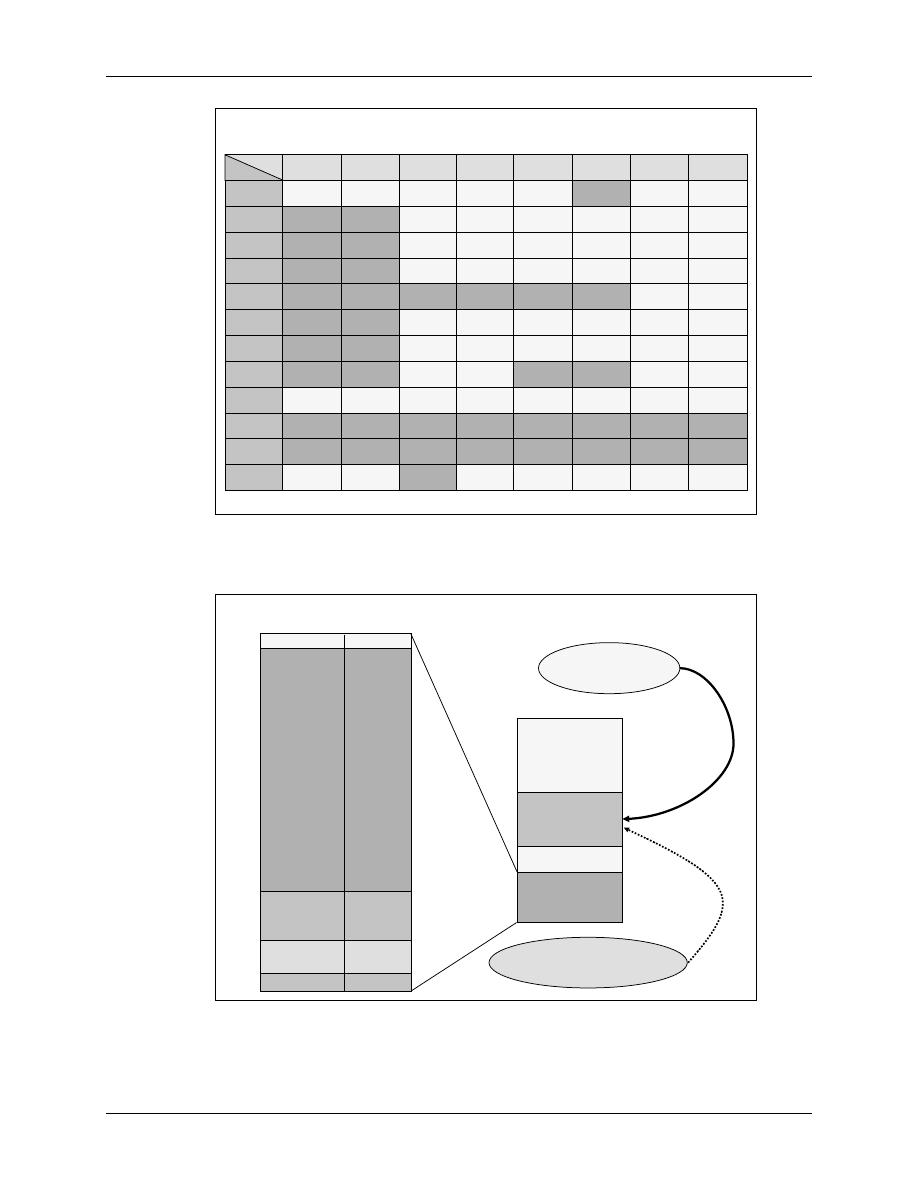
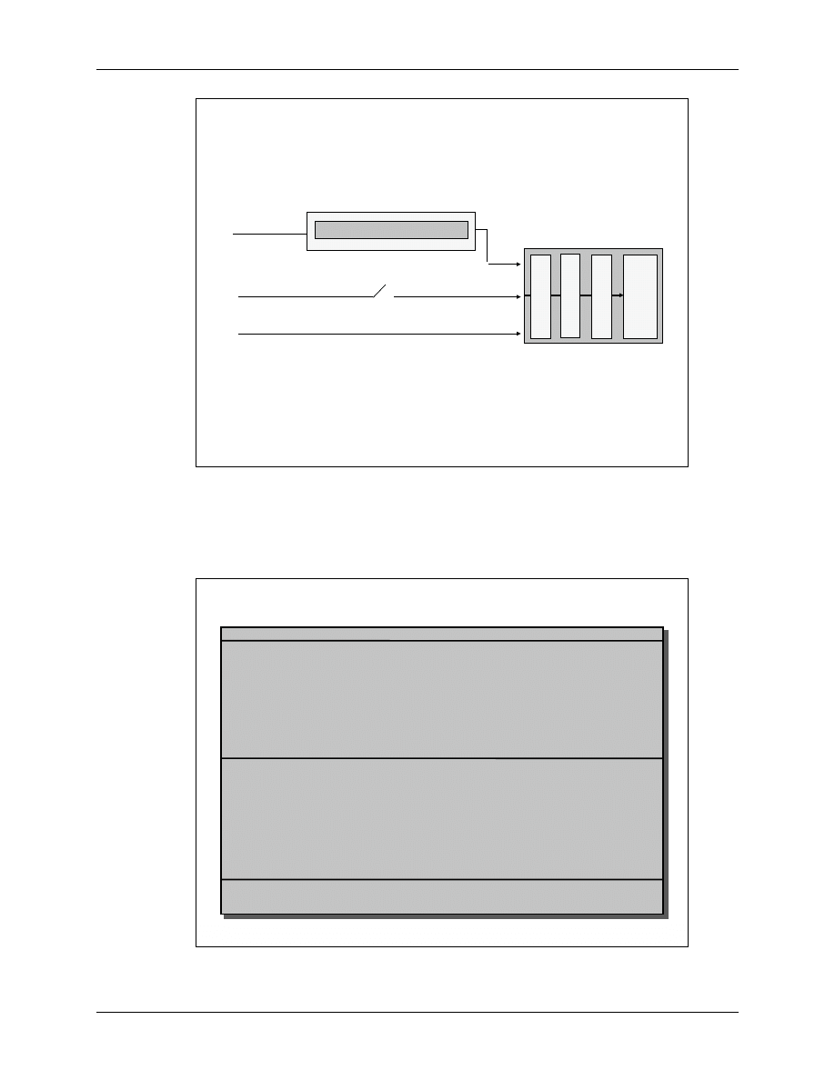
Peripheral Interrupt Expansion
6 - 12
F2833x - Interrupts
Peripheral Interrupt Expansion
All 96 possible sources are grouped into 12 PIE-lines, 8 sources per line. To enable/disable
individual sources we have to program another group of registers: ‘PIEIFRx’ and ‘PIEIERx’.
6
6
-
-
14
14
Peripheral Interrupt Expansion
Peripheral Interrupt Expansion
-
-
PIE
PIE
P
er
ip
h
er
al
I
n
ter
ru
p
ts 12
x8 =
9
6
P
er
ip
h
er
al
I
n
ter
ru
p
ts 12
x8 =
9
6
IFR
IFR
IER
IER
INT
M
INT
M
28x
28x
Core
Core
28x Core Interrupt logic
28x Core Interrupt logic
PIE module for 96 Interrupts
PIE module for 96 Interrupts
INT1.x interrupt group
INT1.x interrupt group
INT2.x interrupt group
INT2.x interrupt group
INT3.x interrupt group
INT3.x interrupt group
INT4.x interrupt group
INT4.x interrupt group
INT5.x interrupt group
INT5.x interrupt group
INT6.x interrupt group
INT6.x interrupt group
INT7.x interrupt group
INT7.x interrupt group
INT8.x interrupt group
INT8.x interrupt group
INT9.x interrupt group
INT9.x interrupt group
INT10.x interrupt group
INT10.x interrupt group
INT11.x interrupt group
INT11.x interrupt group
INT12.x interrupt group
INT12.x interrupt group
INT1
INT1
–
–
INT 12
INT 12
12 Interrupts
12 Interrupts
96
96
INT1.1
INT1.1
INT1.2
INT1.2
INT1.8
INT1.8
1
0
1
•
•
•
•
•
•
•
•
•
•
•
•
INT1
INT1
PIEIFR1
PIEIFR1
PIEIER1
PIEIER1
Interrupt Group 1
Interrupt Group 1
INT13
INT13 (TINT1 / XINT13)
INT14
INT14 (TINT2)
NMI
NMI
6
6
-
-
15
15
PIE Registers
PIE Registers
INTx.2
INTx.2
INTx.3
INTx.3
INTx.4
INTx.4
INTx.5
INTx.5
INTx.6
INTx.6
INTx.7
INTx.7
INTx.8
INTx.8
INTx.1
INTx.1
0
0
1
1
2
2
3
3
4
4
5
5
6
6
7
7
15
15
-
-
8
8
reserved
PIEIFRx register (x = 1 to 12)
PIEIFRx register (x = 1 to 12)
INTx.2
INTx.2
INTx.3
INTx.3
INTx.4
INTx.4
INTx.5
INTx.5
INTx.6
INTx.6
INTx.7
INTx.7
INTx.8
INTx.8
INTx.1
INTx.1
0
0
1
1
2
2
3
3
4
4
5
5
6
6
7
7
15
15
-
-
8
8
reserved
PIEIERx register (x = 1 to 12)
PIEIERx register (x = 1 to 12)
reserved
PIEACKx
PIEACKx
PIE Interrupt Acknowledge Register (PIEACK)
PIE Interrupt Acknowledge Register (PIEACK)
1
1
2
2
4
4
3
3
5
5
6
6
7
7
8
8
9
9
0
0
10
10
11
11
15
15
-
-
12
12
ENPIE
ENPIE
PIEVECT
PIEVECT
PIECTRL register
PIECTRL register
0
0
15
15
-
-
1
1
#include “DSP2833_Device.h”
PieCtrlRegs.PIEIFR1.bit.INTx4 = 1; //manually set IFR for XINT1 in PIE group 1
PieCtrlRegs.PIEIER3.bit.INTx5 = 1; //enable CAPINT1 in PIE group 3
PieCtrlRegs.PIEACK.all = 0x0004; //acknowledge the PIE group 3
PieCtrlRegs.PIECTRL.bit.ENPIE = 1; //enable the PIE
All interrupt sources are connected to interrupt lines according to this assignment table:
Peripheral Interrupt Expansion
F2833x - Interrupts
6 - 13
6
6
-
-
16
16
F2833x PIE Interrupt Assignment Table
F2833x PIE Interrupt Assignment Table
INTx.8
INTx.8
INTx.7
INTx.7
INTx.6
INTx.6
INTx.5
INTx.5
INTx.4
INTx.4
INTx.3
INTx.3
INTx.2
INTx.2
INTx.1
INTx.1
INT1
INT1
WAKEINT
WAKEINT
TINT0
TINT0
ADCINT
ADCINT
XINT2
XINT2
XINT1
XINT1
SEQ2INT
SEQ2INT
SEQ1INT
SEQ1INT
INT2
INT2
EPWM6
EPWM6
_TZINT
_TZINT
EPWM5
EPWM5
_TZINT
_TZINT
EPWM4
EPWM4
_TZINT
_TZINT
EPWM3
EPWM3
_TZINT
_TZINT
EPWM2
EPWM2
_TZINT
_TZINT
EPWM1
EPWM1
_TZINT
_TZINT
INT3
INT3
EPWM6
EPWM6
_INT
_INT
EPWM5
EPWM5
_INT
_INT
EPWM4
EPWM4
_INT
_INT
EPWM3
EPWM3
_INT
_INT
EPWM2
EPWM2
_INT
_INT
EPWM1
EPWM1
_INT
_INT
INT4
INT4
ECAP6
ECAP6
_INT
_INT
ECAP5
ECAP5
_INT
_INT
ECAP4
ECAP4
_INT
_INT
ECAP3
ECAP3
_INT
_INT
ECAP2
ECAP2
_INT
_INT
ECAP1
ECAP1
_INT
_INT
INT5
INT5
EQEP2
EQEP2
_INT
_INT
EQEP1
EQEP1
_INT
_INT
INT6
INT6
MXINTA
MXINTA
MRINTA
MRINTA
MXINTB
MXINTB
MRINTB
MRINTB
SPITXINTA
SPITXINTA
SPIRXINTA
SPIRXINTA
INT7
INT7
DINTCH6
DINTCH6
DINTCH5
DINTCH5
DINTCH4
DINTCH4
DINTCH3
DINTCH3
DINTCH2
DINTCH2
DINTCH1
DINTCH1
INT8
INT8
SCITXINTC
SCITXINTC
SCIRXINTC
SCIRXINTC
I2CINT2A
I2CINT2A
I2CINT1A
I2CINT1A
INT9
INT9
ECAN1
ECAN1
_INTB
_INTB
ECAN0
ECAN0
_INTB
_INTB
SCITXINTB
SCITXINTB
SCIRXINTB
SCIRXINTB
SCITXINTA
SCITXINTA
SCIRXINTA
SCIRXINTA
INT10
INT10
INT11
INT11
INT12
INT12
LUF
LUF
LVF
LVF
XINT7
XINT7
XINT6
XINT6
XINT5
XINT5
XINT4
XINT4
XINT3
XINT3
ECAN0
ECAN0
_INTA
_INTA
ECAN1
ECAN1
_INTA
_INTA
Examples: ADCINT = INT1.6; T2PINT = INT3.1; SCITXINTA = INT9.2
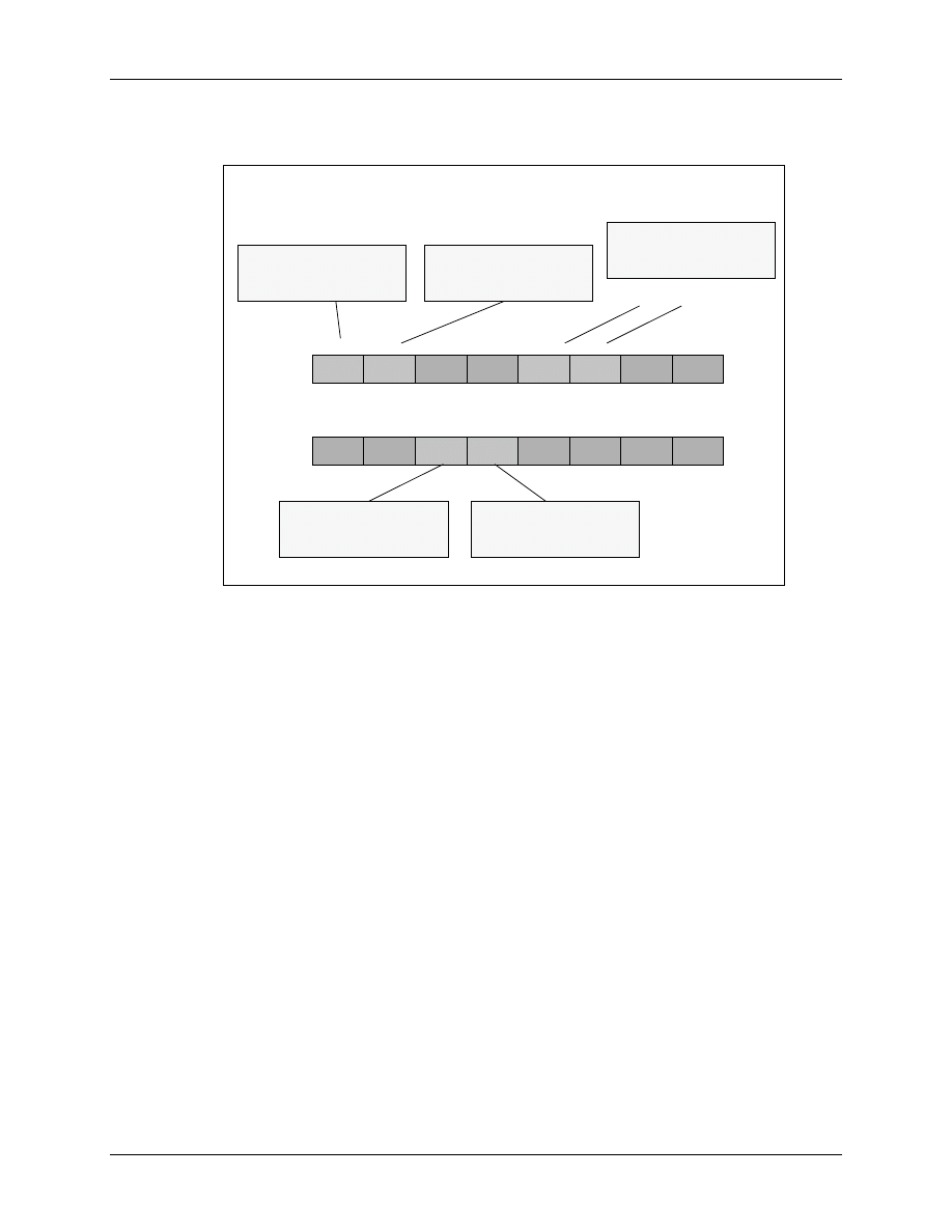
The vector table location at reset is:
6
6
-
-
17
17
Vector
Vector
Offset
Offset
Default Interrupt Vector Table at Reset
Default Interrupt Vector Table at Reset
Memory
Memory
0
0
BROM Vectors
BROM Vectors
64w
64w
ENPIE = 0
ENPIE = 0
0x3F FFC0
0x3F FFC0
0x3F FFFF
0x3F FFFF
PIE Vectors
PIE Vectors
256w
256w
0x00 0D00
0x00 0D00
DATALOG
DATALOG
RTOSINT
RTOSINT
EMUINT
EMUINT
NMI
NMI
02
02
04
04
06
06
08
08
0A
0A
0C
0C
0E
0E
10
10
12
12
14
14
16
16
18
18
1A
1A
1C
1C
1E
1E
20
20
22
22
24
24
26
26
28
28
-
-
3E
3E
ILLEGAL
ILLEGAL
USER 1
USER 1
-
-
12
12
INT1
INT1
INT2
INT2
INT3
INT3
INT4
INT4
INT5
INT5
INT6
INT6
INT7
INT7
INT8
INT8
INT9
INT9
INT10
INT10
INT11
INT11
INT12
INT12
INT13
INT13
INT14
INT14
RESET
RESET
00
00
Default Vector Table
Default Vector Table
Re
Re
-
-
mapped when
mapped when
ENPIE = 1
ENPIE = 1
PieVectTableInit
PieVectTableInit
{ }
{ }
Used to initialize PIE vectors
Used to initialize PIE vectors
The PIE re-maps the location like this:
Peripheral Interrupt Expansion
6 - 14
F2833x - Interrupts
6
6
-
-
18
18
PIE Vector Mapping
PIE Vector Mapping
(ENPIE = 1)
(ENPIE = 1)
PIE vector location – 0x00 0D00 – 256 words in data memory
RESET and INT1-INT12 vector locations are re-mapped
CPU vectors are re-mapped to 0x00 0D00 in data memory
INT13
INT13
0x00 0D1A
0x00 0D1A
XINT13 Interrupt or CPU Timer 1
XINT13 Interrupt or CPU Timer 1
(RTOS)
(RTOS)
INT14
INT14
0x00 0D1C
0x00 0D1C
CPU Timer 2
CPU Timer 2
(RTOS)
(RTOS)
DATALOG
DATALOG
0x00 0D1D
0x00 0D1D
CPU Data logging Interrupt
CPU Data logging Interrupt
……
……
……
……
……
……
USER12
USER12
0x00 0D3E
0x00 0D3E
User
User
-
-
defined Trap
defined Trap
INT1.1
INT1.1
0x00 0D40
0x00 0D40
PIEINT1.1 Interrupt Vector
PIEINT1.1 Interrupt Vector
……
……
……
……
……
……
……
……
……
……
……
……
INT12.1
INT12.1
0x00 0DF0
0x00 0DF0
PIEINT12.1 Interrupt Vector
PIEINT12.1 Interrupt Vector
INT1.8
INT1.8
0x00 0D4E
0x00 0D4E
PIEINT1.8 Interrupt Vector
PIEINT1.8 Interrupt Vector
INT12.8
INT12.8
0x00 0DFE
0x00 0DFE
PIEINT12.8 Interrupt Vector
PIEINT12.8 Interrupt Vector
……
……
……
……
……
……
PIE vector address PIE vector Description
PIE vector address PIE vector Description
not used
not used
0x00 0D00
0x00 0D00
Reset vector (never fetched here)
Reset vector (never fetched here)
Vector name
Vector name
INT1
INT1
0x00 0D02
0x00 0D02
INT1 re
INT1 re
-
-
mapped to PIE group below
mapped to PIE group below
……
……
……
……
……
……
re
re
-
-
mapped to PIE group below
mapped to PIE group below
INT12
INT12
0x00 0D18
0x00 0D18
INT12 re
INT12 re
-
-
mapped to PIE group below
mapped to PIE group below
As you can see from Slide 6-18, the addresses 0x00 0D40 to 0x00 0DFF are used as the
expansion area. Now we do have 32 bits for each individual interrupt vector PIEINT1.1 to
PIEINT12.8.
6
6
-
-
19
19
Device Vector Mapping
Device Vector Mapping
-
-
Summary
Summary
_c_int00:
_c_int00:
. . .
. . .
CALL main()
CALL main()
main()
main()
{ initialization();
{ initialization();
. . .
. . .
}
}
Initialization()
Initialization()
{
{
Load PIE Vectors
Load PIE Vectors
Enable the PIE
Enable the PIE
Enable PIEIER
Enable PIEIER
Enable Core IER
Enable Core IER
Enable INTM
Enable INTM
}
}
PIE Vector Table
PIE Vector Table
256 Word RAM
256 Word RAM
0x00 0D00
0x00 0D00
–
–
0DFF
0DFF
RESET
RESET
<0x3F FFC0>
<0x3F FFC0>
Reset Vector <0x3F F9A9> = Boot Code
Reset Vector <0x3F F9A9> = Boot Code
Flash Entry Point <0x33 FFF6 > = LB _c_int00
Flash Entry Point <0x33 FFF6 > = LB _c_int00
User Code Start < _c_int00 >
User Code Start < _c_int00 >
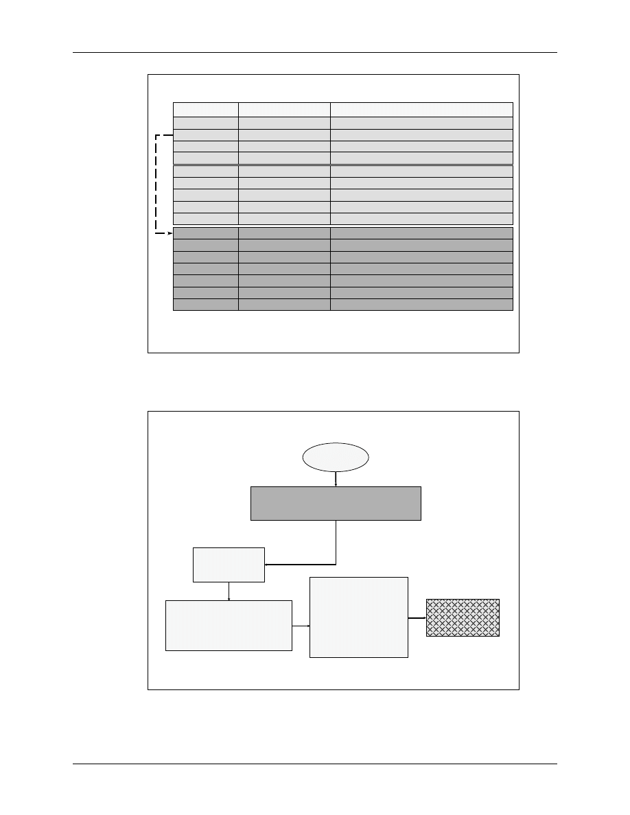
Hardware Interrupt Response
F2833x - Interrupts
6 - 15
Hardware Interrupt Response
After an interrupt has been acknowledged by the CPU, an automatic hardware context switch
sequence is started. It includes an auto-save of 14 internal registers with the all-important internal
control and status bits, and loads the program counter (PC) with the address of the ISR.
6
6
-
-
20
20
Interrupt Response
Interrupt Response
-
-
Hardware Sequence
Hardware Sequence
Note: some actions occur simultaneously, none are interruptible
Note: some actions occur simultaneously, none are interruptible
CPU Action
CPU Action
Description
Description
T
T
ST0
ST0
AH
AH
AL
AL
PH
PH
PL
PL
AR1
AR1
AR0
AR0
DP
DP
ST1
ST1
DBSTAT
DBSTAT
IER
IER
PC(msw)
PC(msw)
PC(lsw)
PC(lsw)
Registers
Registers
→
→
stack
stack
14 Register words auto saved
14 Register words auto saved
0
0
→
→
IFR (bit)
IFR (bit)
Clear corresponding IFR bit
Clear corresponding IFR bit
0
0
→
→
IER (bit)
IER (bit)
Clear corresponding IER bit
Clear corresponding IER bit
1
1
→
→
INTM/DBGM
INTM/DBGM
Disable global ints/debug events
Disable global ints/debug events
Vector
Vector
→
→
PC
PC
Loads PC with int vector address
Loads PC with int vector address
Clear other status bits
Clear other status bits
Clear LOOP, EALLOW, IDLESTAT
Clear LOOP, EALLOW, IDLESTAT
6
6
-
-
21
21
Interrupt Latency
Interrupt Latency
Latency
Latency
Depends on wait states, ready, INTM, etc.
Depends on wait states, ready, INTM, etc.
Maximum latency:
Maximum latency:
Recognition
Recognition
delay (3) and
delay (3) and
SP alignment
SP alignment
(1)
(1)
4
4
Minimum latency (to when real work occurs in the ISR):
Minimum latency (to when real work occurs in the ISR):
Internal interrupts: 14 cycles
Internal interrupts: 14 cycles
External interrupts: 16 cycles
External interrupts: 16 cycles
Get vector
Get vector
(3 reg.
(3 reg.
pairs
pairs
saved)
saved)
3
3
PF1/PF2/D1
PF1/PF2/D1
of ISR
of ISR
instruction
instruction
(3 reg. pairs
(3 reg. pairs
saved)
saved)
3
3
Save
Save
return
return
address
address
1
1
D2/R1/R2 of
D2/R1/R2 of
ISR
ISR
instruction
instruction
3
3
Sync ext.
Sync ext.
signal
signal
(ext.
(ext.
interrupt
interrupt
only)
only)
2
2
cycles
Above is for PIE enabled or disabled
Above is for PIE enabled or disabled
Assumes ISR in
Assumes ISR in
internal RAM
internal RAM
Internal
Internal
interrupt
interrupt
occurs
occurs
here
here
ext.
ext.
interrupt
interrupt
occurs
occurs
here
here
ISR
ISR
instruction
instruction
executed
executed
on next
on next
cycle
cycle
F2833x CPU Timers
6 - 16
F2833x - Interrupts
F2833x CPU Timers
The F2833x features 3 independent 32-bit core timers. The block diagram for one timer is shown
below in Slide 6-22:
6
6
-
-
22
22
F2833x CPU Timers
F2833x CPU Timers
RESET
Timer Reload
SYSCLKOUT
TCR.4
16 - Bit divide down
TDDRH:TDDR
16 - Bit prescaler
PSCH:PSC
32 - Bit period
PRDH:PRD
32 - Bit counter
TIMH:TIM
BORROW
INT
As you can see, the clock source is the internal clock “SYSCLKOUT”, which is usually 150MHz,
assuming an external oscillator of 30MHz and a PLL-ratio of 10/2. Once the timer is enabled
(TCR-bit 4 = 0), the incoming clock counts down a 16-bit prescaler (PSCH: PSC). On underflow,
its borrow signal is used to count down the 32-bit counter (TIMH: TIM). At the end, when this
timer underflows, an interrupt request is transferred to the CPU.
The 16-bit divide down register (TDDRH: TDDR) is used as a reload register for the prescaler.
Each times the prescaler underflows, the value from the divide down-register is reloaded into the
prescaler. A similar reload function for the counter is performed by the 32-bit period register
(PRDH_PRD).
Timer 1 and Timer 2 are usually used by Texas Instruments for the real time operation system
“DSP/BIOS”, whereas Timer 0 is generally free for general usage. Lab 6 will use Timer 0. This
will not only preserve Timer 1 and 2 for later use together with DSP/BIOS, but also help us to
understand the PIE-unit, because Timer 0 is the only timer of the CPU that goes through the PIE,
as can be seen in the following slide, Slide 6-23:
F2833x CPU Timers
F2833x - Interrupts
6 - 17
6
6
-
-
23
23
F2833x Timer Interrupt System
F2833x Timer Interrupt System
IFR
IFR
IER
IER
INT
M
INT
M
28x
28x
Core
Core
28x Core Interrupt logic
28x Core Interrupt logic
PIE unit
PIE unit
INT1.7 interrupt
INT1.7 interrupt
INT1
INT1
TINT1 / XINT13
TINT1 / XINT13
TINT2
TINT2
TINT0
TINT0
INT13
INT13
INT14
INT14
A timer unit is usually initialized by a set of registers. In Lab6, we will perform an exercise with
the registers of CPU Timer 0. However, instead of setting every single bit by ourselves, we will
use a hardware abstraction function, for which we only have to specify the desired timer period
and the clock speed of our processor. This function is provided by Texas Instruments as part of a
set of such functions.
6
6
-
-
24
24
Address
Register
Name
0x0000 0C00
TIMER0TIM
Timer 0, Counter Register Low
0x0000 0C01
TIMER0TIMH
Timer 0, Counter Register High
0x0000 0C02
TIMER0PRD
Timer 0, Period Register Low
0x0000 0C03
TIMER0PRDH
Timer 0, Period Register High
0x0000 0C04
TIMER0TCR
Timer 0, Control Register
0x0000 0C06
TIMER0TPR
Timer 0, Prescaler Register
0x0000 0C07
TIMER0TPRH
Timer 0, Prescaler Register High
0x0000 0C08
TIMER1TIM
Timer 1, Counter Register Low
0x0000 0C09
TIMER1TIMH
Timer 1, Counter Register High
0x0000 0C0A
TIMER1PRD
Timer 1, Period Register Low
0x0000 0C0B
TIMER1PRDH
Timer 1, Period Register High
0x0000 0C0C
TIMER1TCR
Timer 1, Control Register
0x0000 0C0D
TIMER1TPR
Timer 1, Prescaler Register
0x0000 0C0F
TIMER1TPRH
Timer 1, Prescaler Register High
0x0000 0C10 to 0C17 Timer 2 Registers ; same layout as above
F2833x Timer Registers
F2833x Timer Registers
6 - 18
F2833x - Interrupts
It is worthwhile to inspect the control register, as this is the most important register of a timer
unit.
6
6
-
-
25
25
F2833x Timer Control Registers
F2833x Timer Control Registers
TIMERxTCR
TIMERxTCR
Emulator Interaction
1x = run free
0
0
reserved
TRB
1
1
2
2
3
3
4
4
5
5
6
6
7
7
reserved
reserved
TSS
reserved
reserved
reserved
TIE
reserved
FREE
8
8
9
9
10
10
11
11
12
12
13
13
14
14
15
15
reserved
SOFT
reserved
reserved
TIF
Timer Stop Status
0 = start / 1 = stop
Timer Reload Bit
1 = reload
Timer Interrupt Flag
Write 1 clear bit
Timer Interrupt Enable
Write 1 to enable INT
Summary:
Sounds pretty complicated, doesn’t it? Well, nothing is better suited to understand the PIE unit
than a lab exercise. In Lab 6 you will add the initialization of the PIE vector table to re-map the
vector table to address 0x00 0D00. You will also use CPU Timer 0 as a clock time base for the
source code of Lab 5_1 (“2 Bit LED-counter”).
Remember, so far we generated time periods with a software-loop in function “delay_loop()”.
This was quite a waste of processor time, not very precise and poor programming technique.
The procedure on the next page will guide you through the necessary steps to modify the source
code step by step.
Take your time, no pain no gain!
We will use functions, pre-defined by Texas Instruments as often as we can. This principle will
save us a lot of development time; we do not have to re-invent the wheel again and again!

Lab 6: CPU Timer 0 Interrupt and 4 LEDs
F2833x - Interrupts
6 - 19
Lab 6: CPU Timer 0 Interrupt and 4 LEDs
Objective
The objective of this lab is to include a basic example of the interrupt system in the “LED-
counter” project of Lab5_1. Instead of using a software delay loop to generate the time interval
between the output steps, which is a poor use of processor time, we will now use one of the 3 core
CPU timers to do the job. One of the simplest tasks for a timer is to generate a periodic interrupt
request. We can use its interrupt service routine to perform periodic activities OR to increment a
global variable. This variable will then contain the number of periods that are elapsed from the
start of the program.
CPU Timer 0 is using the Peripheral Interrupt Expansion (PIE) Unit. This gives us the
opportunity to exercise this unit as well. Timer 1 and 2 bypass the PIE-unit and they are usually
reserved for Texas Instruments real-time operating system, called “DSP/BIOS”. Therefore we
implement Timer 0 as the core clock for this exercise.
Procedure
Create a Project File
1.
Using Code Composer Studio, create a new project, called
Lab6.pjt
in
C:\DSP2833x\Labs (or in another path that is accessible by you; ask your teacher or a
technician for an appropriate location!).
2.
Open the file Lab5_1.c from C:\DSP2833x\Labs\Lab5 and save it as Lab6.c in
C:\DSP2833x\Labs\Lab6.
3.
Add this source code file to your new project:
•
Lab6.c
4.
From C:\tidcs\c28\dsp2833x\v131\DSP2833x_headers\source add:
•
DSP2833x_GlobalVariableDefs.c
5.
From C:\tidcs\c28\dsp2833x\v131\DSP2833x_common\source add:
•
DSP2833x_CodeStartBranch.asm
6.
From C:\tidcs\c28\dsp2833x\v131\DSP2833x_common\cmd add:
•
28335_RAM_lnk.cmd
7.
From C:\tidcs\c28\dsp2833x\v131\DSP2833x_headers\cmd add:
•
DSP2833x_Headers_nonBIOS.cmd

Lab 6: CPU Timer 0 Interrupt and 4 LEDs
6 - 20
F2833x - Interrupts
8. From C:\CCStudio_v3.3\c2000\cgtools\lib add:
• rts2800_fpu32.lib
9. From C:\tidcs\c28\dsp2833x\v131\DSP2833x_common\source add:
•
DSP2833x_SysCtrl.c
•
DSP2833x_ADC_cal.asm
•
DSP2833x_usDelay.asm
In all Lab5 exercises we used our own function called "InitSystem()" to initialize the core
unit. Now we will use a provided function "InitSysCtrl()" from file "DSP2833x_SysCtrl.c". It
is always good practice to use proven code, there is no reason to re-invent the wheel! The two
other files "DSP2833x_Adc.c" and "DSP2833x_usDelay.asm" define functions, which are
called from functions in file "DSP2833x_SysCtrl.c" - so we have to add these two files to our
project as well.
Project Build Options
10. We also have to setup the search path of the C-Compiler for include files. Click:
Project
Build Options
Select the Compiler tab. In the "Preprocessor" category, find the Include Search Path (-i) box
and enter the following two lines in this box:
C:\tidcs\C28\dsp2833x\v131\DSP2833x_headers\include;
C: tidcs\C28\dsp2833x\v131\DSP2833x_common\include
11. Setup the floating point support of the C - compiler. Inside Build Options select the Compiler
tab. In the "Advanced" category, set "Floating Point Support" to
fpu32
12. Setup the stack size: Inside Build Options select the Linker tab and enter in the Stack Size (-
stack) box:
400
Close the Build Options Menu by Clicking <OK>.
Modify the Source Code
13. Open Lab6.c to edit: double click on “Lab6.c” inside the project window. At the start of your
code, add the function prototype statement for the external function "InitSysCtrl()":
extern void InitSysCtrl(void);

Lab 6: CPU Timer 0 Interrupt and 4 LEDs
F2833x - Interrupts
6 - 21
14. Remove the function prototype for the local function "InitSystem()" at the beginning and the
whole function at the end of Lab6.c
15. In main replace the function call "InitSystem()" by "InitSysCtrl()".
16. Since "InitSysCtrl()" disables the watchdog, but we would like the watchdog to be active, we
have to re-enable the watchdog. Add the following lines just after the call of function
"InitSysCtrl()":
EALLOW;
SysCtrlRegs.WDCR = 0x00AF;
EDIS;
Build, Load and Test
17. Now the new project is ready for build. The code should behave exactly as in Lab5_1, the
four LEDs LD1…LD4 are used to monitor the binary counter. Once more, here are the steps:
Project
Build
File
Load Program
Debug
Reset CPU
Debug
Restart
Debug
Go main.
Debug
Run
If the code does not work as in Lab5_1, do not continue with the next steps! Go back and try
to find out, which step of the procedure you missed.
Modify Source Code - Part 2
18. At the beginning of “Lab6.c” add a function prototype for a new interrupt service function for
CPU Timer 0:
interrupt
void cpu_timer0_isr(void);
19. In “main()”, directly after the function call "Gpio_select()", add a function call to:
InitPieCtrl();
This is a function that is provided by TI’s header file examples. We use this function as it is.
The purpose of this function is to clear all pending PIE-Interrupts and to disable all PIE
interrupt lines. This is a useful step when we would like to initialize the PIE-unit. Function
“InitPieCtrl ()” is defined in the source code file “DSP2833x_PieCtrl.c”; we have to add this
file to our project:
20. From C:\tidcs\c28\dsp2833x\v131\DSP2833x_common\source add to project:
DSP2833x_PieCtrl.c
Also, add an external function prototype at the beginning of Lab6.c:
extern void InitPieCtrl(void);
21. Inside “main()”, directly after the function call “InitPieCtrl();”, add a function call to:

Lab 6: CPU Timer 0 Interrupt and 4 LEDs
6 - 22
F2833x - Interrupts
InitPieVectTable();
This TI-function will initialize the PIE-memory to an initial state. It uses a predefined
interrupt table “PieVectTableInit()” - defined in source code file “DSP2833x_PieVect.c” and
copies this table to the global variable “PieVectTable” -
defined in
“DSP2833x_GlobalVariableDefs.c”. Variable “PieVectTable” is linked to the physical
memory of the PIE area.
Also, add an external function prototype at the beginning of Lab6.c:
extern void InitPieVectTable(void);
To be able to use “InitPieVectTable()”, we need to add two more code files to our project:
22. From C:\tidcs\c28\dsp2833x\v131\DSP2833x_common\source, add to project:
DSP2833x_PieVect.c
and
DSP2833x_DefaultIsr.c
The code file “DSP2833x_DefaultIsr.c” will add a set of interrupt service routines to our
project. When you open and inspect this file, you will find that all ISRs consist of an endless
for-loop and a specific assembler instruction “ESTOP0”. This instruction behaves like a
software breakpoint. This is a security measure. Remember, at this point we have disabled all
PIE interrupts. If we were to now run the program, we should never see an interrupt request.
If, for some reason, for example a power supply glitch, noise interference or just a software
bug, the DSP calls an interrupt service routine, then we can catch this event by the “ESTOP0”
break.
23. Now we have to re-map the entry for CPU-Timer0 Interrupt Service from the “ESTOP0”
operation to a real interrupt service. Editing the source code of TI’s code
“DSP2833x_DefaultIsr.c” would be one way to do this. Of course this would not be a wise
decision, because we would modify the original code for this single Lab exercise. SO DO
NOT DO THAT! A much better way is to modify the entry for CPU-Timer0 Interrupt
Service directly inside the PIE-memory. This is done in main by adding the next 3 lines after
the function call of “InitPieVectTable();”:
EALLOW;
PieVectTable.TINT0 = &cpu_timer0_isr;
EDIS;
EALLOW and EDIS are two macros to enable and disable the access to a group of protected
registers; the PIE is part of this area. The name of our own interrupt service routine for
Timer0 is “cpu_timer0_isr()”. We created the prototype statement earlier in the procedure for
this Lab. Please be sure to use the same name as you used in the prototype statement!
24. Inside “main()”, directly after the re-mapping instructions from above, add the function call
“InitCpuTimers();”. This function will set the core Timer0 to a known state and it will stop
this timer.
InitCpuTimers();
Also, add an external function prototype at the beginning of Lab6.c:
extern void InitCpuTimers(void);

Lab 6: CPU Timer 0 Interrupt and 4 LEDs
F2833x - Interrupts
6 - 23
Again, we use a predefined TI-function. To do so, we have to add the source code file
“DSP2833x_CpuTimers.c” to our project.
25. From C:\tidcs\c28\dsp2833x\v131\DSP2833x_common\source add to project:
DSP2833x_CpuTimers.c
26. Now we have to initialize Timer0 to generate a period of 100ms. TI has provided a function
“ConfigCpuTimer”. All we have to do is to pass 3 arguments to this function. Parameter 1 is
the address of the core timer structure, e.g. “CpuTimer0”; Parameter 2 is the internal speed of
the DSP in MHz, e.g. 150 for 150MHz; Parameter 3 is the period time for the timer overflow
in microseconds, e.g. 100000 for 100 milliseconds. The following function call will setup
Timer0 to a 100ms period:
ConfigCpuTimer(&CpuTimer0, 150, 100000);
Add this function call in “main()” directly after the line InitCpuTimers();
Again, add an external function prototype at the beginning of Lab6.c:
extern void ConfigCpuTimer(struct CPUTIMER_VARS *, float, float);
27. Before we can start timer0 we have to enable its interrupt masks. We have to take care of 3
levels to enable an individual interrupt source. Level 1 is the PIE unit. To enable it, we have
to set bit 7 of PIEIER1 to 1. Why? Because the Timer0 interrupt is directly connected to
group INT1, Bit7. Add the following line to your code:
PieCtrlRegs.PIEIER1.bit.INTx7 = 1;
28. Next, enable interrupt core line 1 (INT1). Modify the register IER accordingly.
IER |= 1;
29. Next, enable interrupts globally. This is done by adding the two macros:
EINT;
and
ERTM;
30. Finally, we have to start Timer 0. The bit TSS inside register TCR will do the job. Add:
CpuTimer0Regs.TCR.bit.TSS = 0;
31. After the end of “main()”, we have to add our new interrupt service routine
“cpu_timer0_isr()”. Remember, we have prototyped this function at the beginning of our
modifications. Now we have to add its body. Inside this function we have to perform two
activities:
1
st
- increment the interrupt counter “CpuTimer0.InterruptCount”. This way we will
have global information about how often this 50 milliseconds task was called.
2
nd
- acknowledge the interrupt service as the last line before return. This step is
necessary to re-enable the next Timer 0 interrupt service. It is done by:
PieCtrlRegs.PIEACK.all = PIEACK_GROUP1;
32. Now we are almost done. Inside the endless while(1) loop of “main()” we have to delete the
function call: “delay_loop(1000000);”. We do not need this function any longer; we can also

Lab 6: CPU Timer 0 Interrupt and 4 LEDs
6 - 24
F2833x - Interrupts
delete its prototype at the top of our code and its function body, which is still present after the
code of “main()”.
33. Inside the endless loop “while(1)“, after the “if-else”-construct, we have to implement a
statement to wait until the global variable “CpuTimer0.InterruptCount” has been incremented
to 1, which corresponds to the interval of 100 milliseconds. Remember to reset the variable
“CpuTimer0.InterruptCount” to zero when you continue after the wait statement.
34. Done?
35. No, not quite! We forgot the watchdog! It is still alive and we removed the service
instructions together with the function “delay_loop()”. So we have to add the watchdog reset
sequence somewhere into our modified source code. Where? A good strategy is to service the
watchdog not in a single portion of our code. Our code now consists of two independent
tasks: the while-loop of main and the interrupt service routine of timer 0. Place one of the two
reset instructions for WDKEY into the ISR and the other one into the while(1)-loop of main.
If you are a little bit fearful about being bitten by the watchdog, then disable it first; try to get
your code running without it. Later, when the code works as expected, you can re-think the
watchdog service part again.
Build, Load and Test
36. Now the new project is ready for final build. The code should behave again exactly as in
Lab5_1, the four LEDs LD1 to LD4 should monitor a binary counter, but now based on a
hardware time base and a working interrupt response system. Here are the steps:
Project
Build
File
Load Program
Debug
Reset CPU
Debug
Restart
Debug
Go main.
Debug
Run
End of Lab6.
Document Outline
- Interrupt System
Wyszukiwarka
Podobne podstrony:
Module 06
Assertivness Module 06
EdPsych Modules PDF Cluster 2 Module 06
CE Elementary module 06 web worksheet
06 BS Module 1 Section 6
06 cisco semestr 2 v31 module 6 exam
06 cisco semestr 3 v31 module 6 exam
06 BS Module 1 Section 6
06 OnScreen B1plus Module 6
MT st w 06
Kosci, kregoslup 28[1][1][1] 10 06 dla studentow
06 Kwestia potencjalności Aid 6191 ppt
06 Podstawy syntezy polimerówid 6357 ppt
06
więcej podobnych podstron