
i
Switch Mode Multilevel (Class D)
Power Amplifier
By
Chiew Tiam Boon
Department of Information Technology and Electrical Engineering
The University of Queensland
Submitted for the
Degree of Bachelor of Engineering (Honours)
In the division of
Electrical Engineering
October 2001

ii
36 Struan Street,
Chapel Hill,
QLD 4069
Tel. (07) 33787247
Mobile no.: 0402404568
October 16, 2001
Simon Kaplan
The Head of
School of Information Technology
And Electrical Engineering.
University of Queensland
St. Lucia 4072
Dear Sir,
In accordance with the requirements of the degree of Bachelor of Engineering (Honour)
in the division of Electrical Engineering, I present the following thesis entitled “Switch
Mode Multilevel (Class D) Power Amplifier”. This work was performed under the
supervision of Dr. Geoffrey R. Walker.
I declare that the work submitted in this thesis is on my own, except as
acknowledgement in the text and footnotes, and has not been previously submitted for a
degree at the University of Queensland or other institution.
Yours sincerely,
Chiew Tiam Boon.

iii
To my family and friends who stood
By me throughout the last four years.
Especially, Lena and her family.

iv
Acknowledgement
Many thanks must go to Dr. Geoffrey Walker for his assistance, guidance and most
importantly for his patient throughout the whole thesis project. Technical assistance
form the Lab supervisor, Peter Allan; Electronic Workshop manager, Barry Daniel also
must be credited
I wish to take this opportunity to thank my course-mates Michael Wortley, Jeffrey
Jordan and Jai Shaw for the continuous support and assistance throughout the whole
progress of this thesis. Especially thank to Lena, for her encouragement and moral
support throughout this whole four years University course.

v
Abstract
Amplifier plays an important role in an audio system. As it simply amplify the input
audio signal to a certain power level to drive the speaker to bring the original desired
signal to live. In recent market, Class AB amplifier seems to be dominating the audio
market. However, when it come to the power efficiency Class D amplifier have a better
output efficiency compare to these classical amplifier (such as class A, B, and AB).
This is base on the fact that, Class D amplifier utilizes the switching operation that the
transistors are either fully on or fully off. Hence, it can achieve the amplification with
zero power dissipation. As a result smaller heat sink is required and amplifier size can
be greatly reduced.
The focus on this thesis is to design a high efficiency, compact size Switch mode
Multilevel (Class D) Power Amplifier. As an amplifier, this design will consist of 3
stages an input stage, gain stage and output stage. Additional control loop is included in
the PWM stage and the overall circuit design to compensate the non-linearities
characteristic of the amplifier.
The result of the design are discussed and follow through to realization, where upon the
effectiveness of each of the implementation is evaluated. These evaluations lead to the
conclusion that the design is able to achieve higher efficiency with low THD <1%.

vi
Table of Content
ACKNOWLEDGEMENT........................................................................................... IV
ABSTRACT....................................................................................................................V
LIST OF FIGURES..................................................................................................... IX
CHAPTER 1....................................................................................................................1
INTRODUCTION – WHAT IS A POWER AMPLIFIER? .......................................1
1.1 C
LASS
D P
OWER
A
MPLIFIERS OPERATION
....................................................1
1.2 R
ECOGNITION OF
P
REVIOUS
W
ORK
................................................................2
1.3 T
HESIS
O
BJECTIVES
...........................................................................................3
1.4 T
HESIS
S
TRUCTURE
...........................................................................................3
CHAPTER 2....................................................................................................................5
BACKGROUND .............................................................................................................5
2.1 T
HE
D
IFFERENT BETWEEN THE
L
INEAR
M
ODE AND
S
WITCH
M
ODE
A
MPLIFIER
..................................................................................................................5
2.2 T
YPE OF
A
MPLIFIER
...........................................................................................6
2.2.1 Class A Amplifier
.......................................................................................6
2.2.2 Class B Amplifier
.......................................................................................7
2.2.3 Class AB Amplifier
....................................................................................7
2.2.4 Class D Amplifier
......................................................................................7
2.3 I
MPLEMENTATION ON THE
C
LASS
D
AMPLIFIER TO IMPROVE IT
PERFORMANCE
...........................................................................................................8
2.3.1 Multilevel Switching
.................................................................................8
2.3.2 Output filter design
...................................................................................8
2.3.3 Close loop control
.....................................................................................9
CHAPTER 3..................................................................................................................11
DESIGN THEORY.......................................................................................................11
3.1 S
WITCH
M
ODE
C
ONVERTERS
.........................................................................11

vii
3.2 P
ULSE
W
IDTH
M
ODULATION
(PWM)
TECHNIQUE
....................................12
3.3 C
LASS
D
OPERATION
.......................................................................................14
3.3.1 Multilevel Switching
...............................................................................14
3.4 C
HARACTERISTICS OF
C
LASS
D
AMPLIFIER
................................................15
3.4.1 Switching and conduction Losses
........................................................15
3.4.2 Shoot-Through
..........................................................................................16
3.4.3 Output filter – Demodulation of the PWM
........................................17
3.5 S
TABILITY OF THE
C
LOSE
L
OOP CONTROL SYSTEM
..................................17
3.5.1 Pole Location – Root Loci
.....................................................................17
3.5.2 Gain and Phase Margins
.......................................................................18
CHAPTER 4..................................................................................................................20
IMPLEMENTATION ..................................................................................................20
4.1 I
NPUT
S
TAGE
.....................................................................................................20
4.1.1 Carrier Generation
.................................................................................20
4.1.2 Input Pre-amplifier and Subwoofer filter stage
...............................25
4.2 P
ULSE
W
IDTH
M
ODULATION
(PWM) S
TAGE
............................................25
4.3 I
NNER
L
OOP
(
CLOSE LOOP CONTROL FOR THE
PWM)
..............................26
4.4 H-B
RIDGE
MOSFET
AND
H-
BRIDGE
MOSFET
DRIVER CIRCUIT
.........26
4.5 C
ENTER
T
APPED
T
RANSFORMER FOR MULTIPLE OUTPUTS
......................27
4.6 O
UTPUT
F
ILTER STAGE
....................................................................................28
4.7 O
VERALL
C
LOSE LOOP DESIGN
.....................................................................30
CHAPTER 5..................................................................................................................32
DESIGN RESULT AND DISCUSSION.....................................................................32
5.1 R
ESULT ON THE
C
ARRIER GENERATION STAGE
..........................................32
5.2 R
ESULT FROM THE
PWM
STAGE
..................................................................35
5.3 T
HE POSSIBLE FAILURE STAGE
.......................................................................36
5.3.1 H-Bridge MOSFET driver chip (
HIP4082
) and H-bridge configuration ...37
CHAPTER 6..................................................................................................................39

viii
CONCLUSION .............................................................................................................39
6.1 F
UTURE WORK
..................................................................................................39
APPENDIX A.................................................................................................................. I
SCHEMATIC DIAGRAMS........................................................................................... I
APPENDIX B ............................................................................................................... IV
PCB LAYOUT ............................................................................................................. IV
APPENDIX C.................................................................................................................V
BIBLIOGRAPHY..........................................................................................................V

ix
List of Figures
Figure 1-1: Conceptual Topology of a Class D Power Amplifier...............................2
Figure 2-1: Class A amplifier.........................................................................................6
Figure 2-2: Class B amplifier.........................................................................................7
Figure 2-3: Class AB design...........................................................................................7
Figure 2-4: Class D amplifier.........................................................................................8
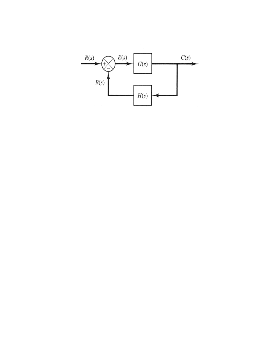
Figure 2-5: Generic close loop control system block diagram....................................9
Figure 3-1: The Buck Converter .................................................................................12
Figure 3-2: Naturally Sampled Carrier Based PWM [4]..........................................13
Figure 3-3: Interleaved Switching topology [4]..........................................................15
Figure 3-4: Gain and Phase margin base on the bode diagram [12, p.546] ............19
Figure 4-1: Block Diagram for the Class D amplifier Design with close loop system
................................................................................................................................20
Figure 4-2: 1MHz Clock pulse generating circuit from a crystal [17, 4-25]............22
Figure 4-3: Frequency Divider circuit (a) and the timing diagram (b) [4]..............23
Figure 4-4: Common Integrator circuit by using an OP-Amp.................................24
Figure 4-5: The input Low Pass Filter and Pre-Amp stage circuit [1] ....................25
Figure 4-6: H-Bridge MOSFET topology...................................................................27
Figure 4-7: Derivation on transformer Bobbin pin out ............................................28
Figure 4-8: LC low Pass Filter half-circuit model .....................................................29
Figure 4-9: Combination of two Half-Circuit Models...............................................29
Figure 4-10: Feedback and error amplifier (error compensate) circuit..................31
Figure 5-1: Output from Frequency divider circuit (1) 125 KHz and (2) 500 KHz
square waveform generate from 1MHz ..............................................................33
Figure 5-2: The 125 KHz square waveform (clock pulse) generate through the use
of Frequency divider circuit. Four 90û-phase shifted square waveform. ........34
Figure 5-3: The Triangular waveform integrated from the four 90û-phase shifted
125 KHz square waveforms. ................................................................................35
Figure 5-4: Generation of PWM waveform on a 100Hz input signal with a 1KHz
triangular waveform. (a) Both input signal and Carrier frequency (b) The
non-inverting output from LM361 (c) The inverting output from LM361.....36

1
Chapter 1
Introduction – What is a Power Amplifier?
An amplifier is capable of delivering a large amount of power to the output load
without any losses incur in the process. Among the existing audio amplifier, most of the
classical amplifier such as Class A, AB and those linear device amplifier, their power
efficiency can only achieve up to 70~80% at most, since most of the power was wasted
as a heat dissipation. However, with Class D amplifiers, they are based on the switch
mode operation, which can achieve a theoretical 100% power efficiency. DU to the fact
that there is virtually no (zero) power dissipation occur in the operation, the system
(circuit design) can be reduce to a compact size, as bulky heat sink element is not
crucially in need.
1.1 Class D Power Amplifiers operation
As mentioned earlier, Class D amplifier can greatly reduce the power losses in the
circuit. As the transistors in the Class D amplifier design are either on or off through out
the operation which reduced their linear region to a finite switching time between
saturation and cut-off. That the major different compare to the classical amplifier. Due
to the recent portable audio market, computer multimedia access (especially the arising
MP3 digital audio file) as well as the need for the car audio system, the demand for a
high efficiency power amplifier is very high. Since if there exist no power dissipation in
the circuit design (in this case the power amplifier), the power supply will be efficiently
deliver a full power to the output stage thus power supply are fully utilise as required
instead of wasting through the heat dissipation which only produce heat but nothing
useful.
The following figure shown the theoretical conceptual Class D amplifier topology,
which break into 4 major parts, such as input stage, PWM (Pulse Width Modulation)
stage, Amplifying (H- Bridge MOSFET configuration) stage and output stage.
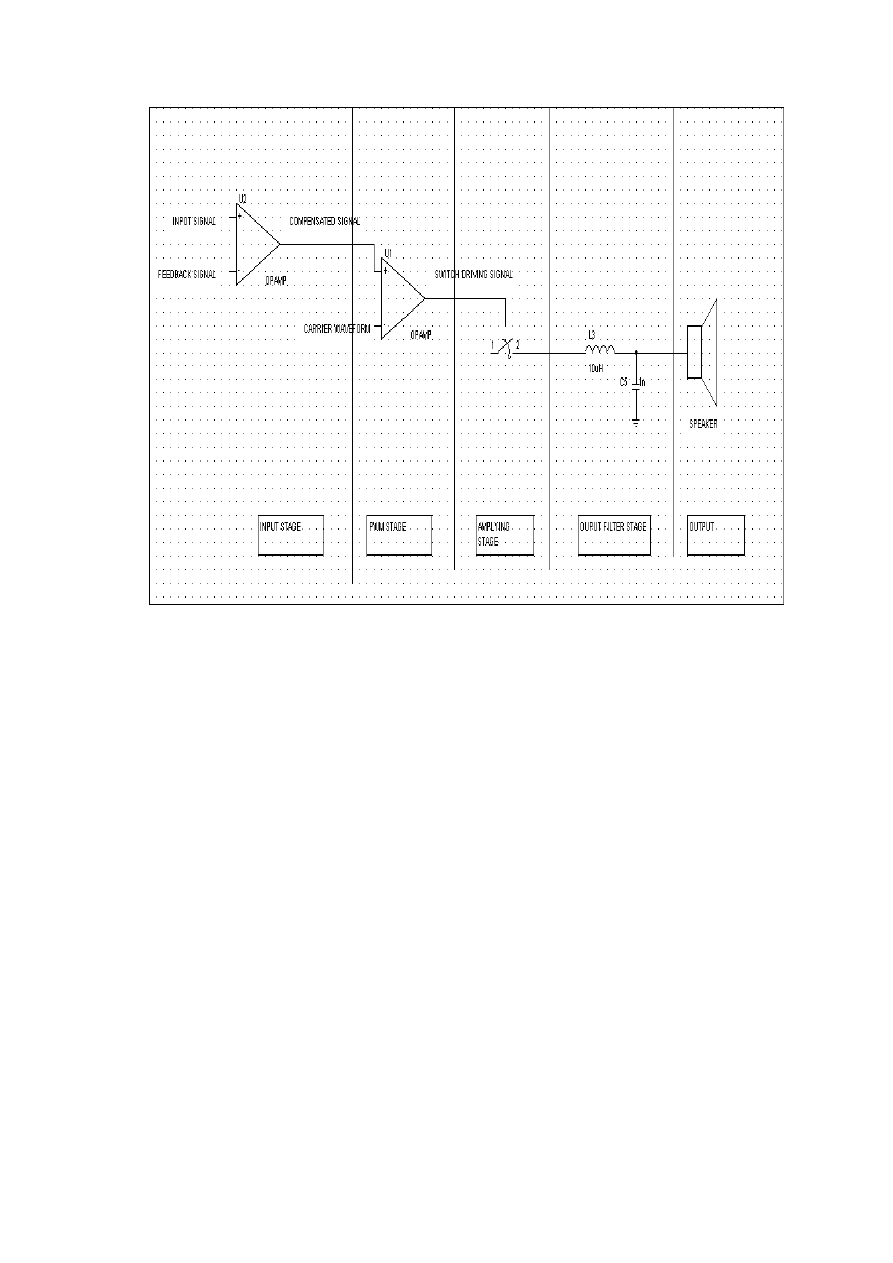
2
Figure 1-1: Conceptual Topology of a Class D Power Amplifier
This operation is somehow similar to the DC-DC switch mode converters operation. As
in both operations, the input signal is modulated using the PWM (Pulse Width
Modulation) method. That is, the input signal was modulated such that the duty ratio of
the modulated signal is proportional to the instantaneous input voltage. This modulated
signal is then use to drive a switch (or a set of switches) to perform/produce an
amplified PWM waveform. This amplified and modulated waveform is then fed into the
output stage where demodulation of the modulated signals takes place. Usually this
stage will consist of an output filter to perform the demodulation task.
Theoretically, Class D amplifier can produce an impressive 100% power efficiency.
However, in the practical mode that is impractical to achieve that due to the
imperfection in both circuit and design realization.
1.2 Recognition of Previous Work
The basic concept and design approach of this thesis project was references from the
past year thesis. They are 1998, Multilevel Switch Mode Class D Power amplifier,
authored by Tng Chee Wan and in 1999, Christopher N. Hemmings’ Improving Class D

3
Audio Amplifier. Where in Tng’s thesis, an open loop 3-level Class D amplifier was
design with 94% power efficiency. While in 1999, Hemmings’ thesis project
implement on Tng’s 3 level Class D amplifiers with an addition close loop design to
compensate the inherent nonlinearities as well as the distortion problem in the amplifier
design.
1.3 Thesis Objectives
The main objectives of the thesis project are to design and construct a compact size,
workable, Switch Mode 5-level (Class D) Power amplifier for a car audio system – a
subwoofer application. The power supply voltage will be range about 12V and an
output load resistance of 4ohms will be used, as a speaker thus an output power around
30W will be expected. By applying the used of the multilevel interleaving technique
(based on Tng’s and Hemmings’ thesis techniques) the audio quality (high fidelity) of
the Class D amplifier design will be increased. The design will based on the existing
Class D amplifier and implement on the close loop control system, such as the inner
feedback loop in the PWM modulator stage as well as an outer feedback loop for the
whole Class D amplifier design. With this implementation the design will be able to
produce a higher fidelity performance and eventually reduce the nonlinearities and
distortion characteristic in the design. On the other hand, the shoot through loss that will
arise in the H-Bridge MOSFET transistor will be avoided by using the HIP4082I H-
Bridge MOSFET Driver, which comes with a programmable dead time. Detail will be
cover in the Design Theory Section.
1.4 Thesis Structure
After a brief introduction on this thesis, Chapter 2 will provide an overview of the
development of the classical amplifier such as Class A and AB, as well as the digital
audio amplifier, Class D amplifier. Their general operation and performance will be
stated and comparison between these classical amplifiers and the switch mode amplifier
will also be discussed. This will be mainly focus on the power efficiency of the
particular amplifier and their audio fidelity performance. Discussion on the advantages
and disadvantages on the Class D amplifier will also be included in Chapter 2.
While in Chapter 3, summary of the design theory that will be used in designing this
Class D amplifier will be stated. These include the derivation of Class D operation

4
concept from a DC-DC converter, method of PWM, output filter design consideration
and close loop control.
While the detail of the design approach and components selection will be stated in the
Chapter 4. In Chapter 4, the design approach will break into difference stages
accordingly. From the input stage – Preamplifier, oscillator generation stage, PWM
stage, inner feedback loop, H-Bridge and H-Bridge MOSFET Driver chip, output filter
stage as well as the close loop control for the entire circuit design will be enclosed.
In chapter 5, the result obtain from the testing of the design will be discussed. Based on
these results, discussion on the close loop design as well as the circuit performance will
be stated.
While in chapter 6, based on the testing result from chapter 5, it is concluded that the
close loop system is able to increase the performance of the existing Class D amplifier.

5
Chapter 2
Background
An Amplifier being as an important element in an audio system since it amplifies the
input signal to a certain desired power to drive the speaker. However, there still don’t
exist an amplifier that can deliver the full input power to the output load i.e. 100%
power efficiency operation. Even though the dominating class AB amplifier, the most it
can achieve are around 70% ~ 80%. A Class D amplifier theoretically can achieve this
high efficiency situation provided there is an idea transistor that with no turn-on
resistance and etc. Although the output efficiency of a class D amplifier can be higher
than Classical amplifier, yet its distortion level is higher than the classical amplifier.
Hence, the class D amplifier is being limited to a few applications only such as
subwoofer system. On the other hand, due to the fact that most of the classical
amplifiers are huge in side and weight (heat sink required) which make the Switch
mode Class D amplifier become popular in demand for the portable personal audio
system. Such as mobile phone, PC audio system and smaller size audio system. Since
the Class D operation required only a smaller size of heat sink compare to the classical
amplifier. Furthermore, due to it superior performance on the output power efficiency,
battery operates system make it even better for implementation. However, the draw
back is that design for this kind of amplifier is very complicated compare to those
classical amplifiers.
2.1 The Different between the Linear Mode and Switch Mode
Amplifier
Most of the circuit element can be classified into resistive, capacitive element, magnetic
devices including inductor and transformer, and semiconductor devices operate in linear
mode or switch mode. If a circuit is operating in a linear mode, usually they operate
under the conventional signal processing application where frequency is not the primary
concern. Hence, magnetic devices can be avoided in linear mode operation. Since the
output of a linear mode operation is in a linear relationship with the input where the
output is directly derived from it thus it is able to provide a minimal output distortion.
However, since the transistor is operating in its linear region (on stage) all the time thus

6
potentially high power dissipation will be resulted. This will directly affect the
efficiency of the circuit since some of the power is being wasted through the heat
dissipation into the air (surrounding). Classical amplifiers such as Class A, B and AB
are operate in the linear mode as the output transistor is operate in the linear region
[11].
In contrast, capacitor and magnetic devices those play an important role in a switch
mode operation, as ideally they consume no power. As a result, resistive elements and
semiconductor that operate in linear mode was avoided, while switch mode
semiconductor devices are employed. In this switch mode operation, the semiconductor
devices are either fully on (saturation region) or off (cut-off region) stage. It is this
operation mode that results the theoretical zero power dissipation. Since in a cut-off
region, there is not current flow and in the saturation region there is not voltage drop in
the semiconductor device. However, practically these semiconductors do experience
some power loss in these regions due to leakage currents and conduction voltage, yet
when compare these losses to linear mode operation, they are quite small. The most
significant power loss in this operation mode was the switching losses – transition
between the cut-off region and saturation region [11].
2.2 Type of Amplifier
2.2.1 Class A Amplifier
Class A operation is where both devices conduct continuously for the entire cycle of
signal swing, or the bias current flows in the output devices all the times. The key
ingredient of Class A operation is that both devices are always on. There is no condition
where one or the other is turned off. Because of this, Class A amplifiers are single-
ended designs with only one type of polarity output devices. Class A is the most
inefficient of all power amplifier designs, averaging only around 20%. Because of this,
Class A amplifiers are large, heavy and run very hot. All this is due to the amplifier
constantly operating at full power. The positive effects of all this is that Class A design
are inherently the most linear, with the least amount of distortion [18]. Here is the
Class A amplifier design (topology).
7
Figure 2-1: Class A amplifier
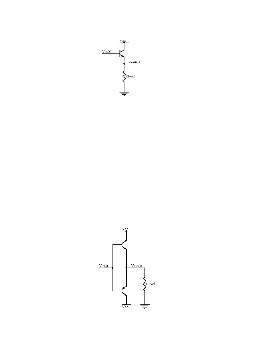
2.2.2 Class B Amplifier
Class B operation is opposite of Class A. Both output devices are never allowed to be
on at the same time, or bias is set so that current flow in a specific output device is zero
when not stimulated with an input signal, i.e., the current in a specific output flows for
one half cycle. Thus each output devices is on for exactly one half of a complete
sinusoidal signal cycle. Due to this operation, Class B designs show high efficiency but
poor linearity around the crossover region. This is due to the time it takes to turn one
device off and the other device on, which translates into extreme crossover distortion.
Thus restricting Class B designs to power consumption critical applications, e.g. battery
operated equipment such as 2-way radio and other communications audio [18]. Here is
the Class B amplifier design.
Figure 2-2: Class B amplifier
8
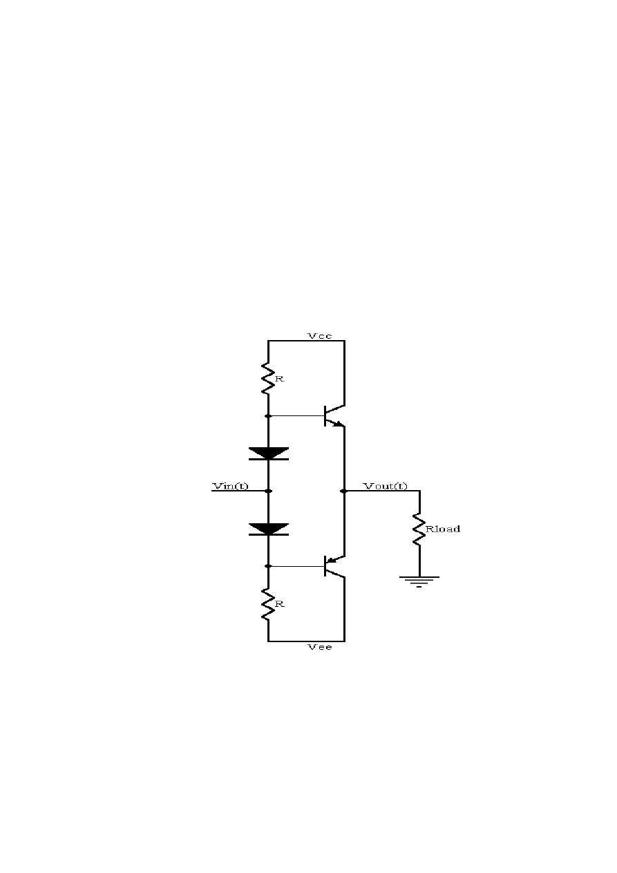
2.2.3 Class AB Amplifier
Class AB operation allows both devices to be on at the same time (Like Class A), but
just barely. The output bias is set so that current flows in a specific output device
appreciably more than a half cycle but less than the entire cycle. That is, only a small
amount of current is allowed to flow through both devices, unlike the complete load
current of Class A design, but enough to keep each device operating so they respond
instantly to input voltage demands. Thus the inherent non-linearity of Class B designs is
eliminated, without the gross inefficiency (50%) with excellent linearity that make class
AB the most popular audio amplifier design [18]. Here the Class AB designs.
Figure 2-3: Class AB design
2.2.4 Class D Amplifier
Class D operation is switching, hence the term switching power amplifier. Here the
output devices are rapidly switched on and off at least twice for each cycle (Sampling
Theorem). Theoretically since the output devices are either completely on or completely
9
off they do not dissipate any power. Consequently class D operation is theoretically
100% efficient, but this requires zero on-impedance switches with infinitely fast
switching times – a product we’re still waiting for; meanwhile designs do exist with
true efficiencies approaching 90% [18]. The following figure is the Class D amplifier
design.
Figure 2-4: Class D amplifier
2.3 Implementation on the Class D amplifier to improve it
performance
2.3.1 Multilevel Switching
This technique will be based on the past year Thesis design technique – interleaved
switching converters [4, 5]. That is placement of several similar design two-level
converter in parallel and driven them with the phase shifted PWM waveforms [5]. The
generation of drive signals is achieved by comparison of the input signal with the phase
shifted carrier waveform separated by equally spacing in 360. This will result in a
generation of multilevel PWM signal being present to the output filter. The advantages
of this technique are there is a reduction in ripple amplitude and increase in effective
ripple frequency [9]. Eventually, this will allow the output filter to be more effective in
demodulating the PWM signal.

10
2.3.2 Output filter design
In a Class D amplifier design, the output from the H-bridge is a square waveform
(pulsed waveform). Hence, in order to drive the speaker, the output waveform has to be
at least a sine waveform thus this output waveform has to be reconstructing back to its
original input signal. Traditionally, a LC low pass filter can be used to achieve the
requirement, yet this can be result in some design difficulties. Based on the past year
basic design rules established by many Class D designers, the following concepts can
be used as a general guide for designing the output filter stage. [4]
! Filter need to be constant amplitude and linear phase response within the audio
bandwidth. By maintaining this condition the distortion level will be minimized.
! To minimal the power losses, filter have to be design in passive elements. The
power efficiency can be increased if the power losses are minimized. Since the
resistive element prone to dissipate power proportional to its resistance value.
! Filter must be able to attenuate the carrier frequency (modulating frequency)
and its harmonics from the output waveform. Obviously the output frequency
needed is just the audio bandwidth thus non-audio frequency must be removed.
2.3.3 Close loop control
By definition, a Close loop control system always implies the uses of feedback control
action to reduce the system error. While the definition of an open loop system is the
output has no effect on the control action. The advantage of a close loop control system
compare to an open loop control system is in fact use the feedback makes the system
response relatively insensitive to external disturbances and internal variations in the
system parameter. However, the system stability is a major problem in a close loop
control system, as overcorrecting the error might tend to cause oscillations of constant
or changing amplitude.
11
Figure 2-5: Generic close loop control system block diagram
In a practical Class D amplifier design, there still consist of unavoidable imperfection in
the PWM stage as well as the output stage. These are non-linear characteristic of the
design, which will cause the harmonic distortion as well as the other form of distortion
to arise. In order to compensate these imperfections, close loop control system will be
incorporated to solve/correct these problems. However, as mentioned earlier, the design
on the close loop control system must be carefully considered. Instability of the close
loop system will cause the output oscillate with or varying amplitude.

12
Chapter 3
Design Theory
In this chapter, relevant design theory will be stated and explained. The design of the
Class D amplifier will be based on these design requirements to implement.
3.1 Switch Mode Converters
As mentioned earlier in the Chapter 1 and 2, the Class D amplifier operation is based on
the switch mode operation, which is derived from the Switch Mode Converter. These
Switch Mode Converters can be divided into four main categories, i.e. DC-DC
converters, DC-AC inverters, AC-DC rectifiers or inverters and AC-AC. While the
Class D amplifiers are fall into the AC-AC converter category. Since the input and
output is expected to be sinusoidal waveform.
The average output voltage of a DC-DC converter with a given input voltage is
controlled by controlling the switch on and off duration (t
on
and t
off
). Through this
control method the average output voltage can be controlled to equal a desire level,
while the input voltage and the output load may be fluctuated. By applying the PWM
technique, the signal level control voltage compare with a repetitive waveform
(constant frequency) and generate the switch duty ratio. The transfer function for the
DC-DC converter can be represented by the Equation 3-1.
s
in
on
V
V
T
t
D
=
=
Equation 3-1
Where this repetitive waveform frequency is usually high enough for the inductor and
capacitor at the output filter stage to average out this switching frequency and providing
the above mentioned constant output voltage.
A DC-DC switch mode converter operation can be illustrated by the simple
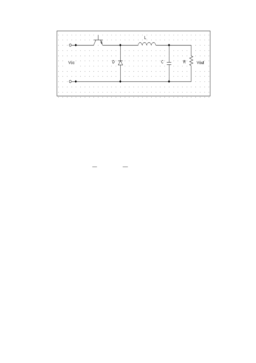
implementation of a Buck (or step down) Converter.
13
Figure 3-1: The Buck Converter
In this Buck converter circuit, the BJT was switched between it on and off state by the
controlled signal (Duty ratio) to keep the output voltage maintain at a desire level. The
relationship between the average output for an idea Buck converter (assumed purely
resistive load and ideal switch) and the input voltage can be calculated in term of the
switch-duty ratio [10, p.164]:
d
d
s
on
Ts
o
s
o
DV
V
T
t
dt
t
v
T
V
=
=
=
∫
0
)
(
1
Equation
3-2
From Equation 3-2, we know that if we can alter the switching duty ratio, the gain of
the Buck converter can be easily manipulated.
3.2 Pulse Width Modulation (PWM) technique
In order to perform the switch mode operation amplifier, Pulse Width Modulation
technique plays the basic principle in the design. The pulse width of the PWM
waveform is varied proportionally to the input audio signal to control the output
voltage. Most of the PWM techniques can be categorize into three main area, they are:
•
Hysteresis Control
Operate as a feedback control loop. The desired output level was compared
with the instantaneous output level; a hysteresis modulator control produces
an error signal to control the output switches. The advantages of this
technique are it offers bounded and predictable error and fast transient
response. Moreover, it presents low distortion and easy implementation.
Disadvantages are the output-switching period is not constant, which cause
the output filter very hard to implement [4, 5].
14
•
Pre-calculated PWM techniques
It is performed offline and often used in selected harmonics elimination. Yet,
due to irregular pulses occurrence, it can’t promptly response to the circuit
transient. Hence, it is not suitable for Class D amplifier implementation [4, 5].
•
Carrier based PWM
This techniques use a fixed frequency to sample the input waveform, which
match the Class D amplifier implementation perfectly. There consist of two
main types of carrier based PWM i.e. natural sampling uniform sampling.
These two different sampling types have some similarity however, natural
sampling doesn’t have any delay between sampling of the input and output
response reflecting this input values. As a result, natural sampling method
doesn’t introduce any harmonic distortion. Unlike natural sampling, uniform
sampling method have a finite delay occurrence which caused an undesired
odd harmonics appear within the output spectrum [4, 5].
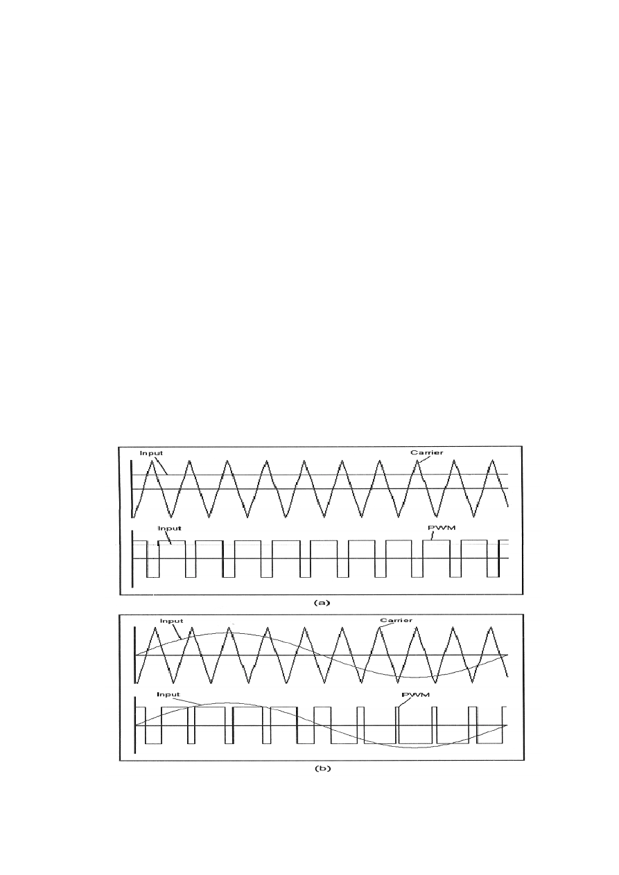
The following figure will give a clear view on the natural sampling Carrier Based
PWM.
Figure 3-2: Naturally Sampled Carrier Based PWM [4]

15
A constant amplitude input voltage was compared to the triangular carrier frequency
and produces a constant duty ratio modulated PWM waveform (pulse-train). While a
sinusoidal waveform input waveform was compared, the modulated output having an
instantaneous duty ratio proportional to the instantaneous input voltage. This
relationship can be shown as the following equation.
Constant
=
in
V
D
(k) Equation
3-3
In order to remain the linearity relationship between the input voltage and output duty
ratio and distortion-free, the carrier frequency must consist only a straight-line segment.
Furthermore, the consistency of the carrier frequency waveform must also be
maintained to ensure the demodulation process can be implemented effectively.
3.3 Class D operation
If the Buck converter (Figure 3-1) can be controlled by a PWM waveform shown in
Figure 3-2 (b), the transfer function can be shown as follow:
cc
out
in
kV
V
V
=
Equation
3-4
The Buck converter can be treated as a linear mode voltage amplifier if V
cc
is treated as
constant. That is how the Class D amplifier operation based on. Furthermore, if varying
the V
cc
, the gain of the amplifier can be modified [4].
In a Buck converter, a unidirectional single–quadrant switch is used as a switch, which
is a common used in DC-DC converter. However, in a Class D amplifier, which is in a
dc-ac inverters application, a Bi-directional two-quadrant switch must be used. Since
the switching elements conduct currents in both polarities, but block only positive
voltages [11]. The MOSFETs will make the choice for this application since them
inherent the low drive losses [4].
3.3.1 Multilevel Switching
The interleaving theory on multilevel switching based on Tng’s and Hemming’s thesis
will be referenced here as well. Here is the basic topology of multilevel interleaving
techniques after Hemmings [4].
16
Figure 3-3: Interleaved Switching topology [4]
The interleaved signals were 90û-phase shifted between each other in order to minimal
the harmonic distortion and achieved the multilevel switching. With the equally spacing
these carrier through out one cycle by a 360û/n phase shifted, an n+1 level of PWM
waveform presented in the output filter.
3.4 Characteristics of Class D amplifier
3.4.1 Switching and conduction Losses
Even though it is (theoretically) proved that Class D amplifier can achieve 100% power
efficiency, yet in practical there is not such thing as 100% efficiency. Since there still
haven’t found any ideal switches for this application. Most of the switches will consist
some power losses during its conduction period as well as the in its switching stage.
Thus when a non-ideal switches is in used; there will be some losses occur during the
operation, such as switching losses and conduction losses. These are the most
significant losses in the switch mode transistors.
Switching losses is occur during the transition period, which is the period when the
transistor changing from it saturation mode to cut-off mode. Hence, switching losses as
the name said it all is proportional to the switching frequency. During this transition,
there is a finite rise and fall time in both voltage and the current. Since it is non-ideal

17
case, the existence of this non-zero value of voltage and current will eventually result
power dissipation in the transition. By reducing the switching frequency, the switching
losses can be reduced to the following equation.
)
(
)
(
(
2
1
off
t
on
t
f
I
V
P
c
c
s
o
d
s
+
=
Equation 3-5 [10, p.23]
Where t
c
is the conduction period during the on and off state,
s
f is the switching
frequency. However, reducing the switching carrier will increase the difficulties on
demodulating it at the output filter stage (hard to design a proper filter to filter off the
carrier frequency if the fundamental frequencies are close to the carrier frequency). If
the switching losses can be effectively managed the following losses will become
dominant factor in the amplifier’s efficiency. While the switch is on (saturation region)
there exists a non-zero voltage across the switch. Since there is a voltage across the
switch, there will be a current flowing through the switch as well. When coupled this
voltage and current, it result the conduction losses of the switch. This conduction loss is
only occurring within the saturation region duration (switch is on condition) thus this
loss is proportional to the switching duty ratio as shown in the following Equation 3-6.
s
on
o
on
on
T
t
I
V
P
=
Equation 3-6 [10, p.23]
Where, T
s
is the switching period
s
f
1
and t
on
is the switch on duration. In order to
reduce the conduction losses, even it is not that significant; the forward voltage of the
transistor must be considered. In a MOSFET, this can be figured out from its turn-on-
resistance i.e. the smaller the resistance the smaller the conduction losses.
3.4.2 Shoot-Through
Shoot-through loss is one specific type of switching losses. It occur when the half
bridge (or full- bridge) transistor are both conduct. This shoot through loss can be
avoided by implementing a dead time between the turning off one MOSFET and
turning on the other. Furthermore, with the implemented dead time, the cross over
distortion can also be prevented [6].

18
3.4.3 Output filter – Demodulation of the PWM
As mentioned earlier in chapter 2, the pulsed waveform (output waveform) output from
the H-bridge MOSFET transistors cannot be applied to drive the speaker. Thus the
output waveform has to be reconstructed back into a sine waveform (similarly) in order
to perform the amplified audio signal. Form section 2.5.2, in the previous chapter, based
on the past year experience from Class D amplifier designer, a low pass filter will suit
for this application. Since the audio bandwidth is ranged from 20 Hz ~ 20 KHz, while
the carrier frequency is normally more than 5 time higher than the audio frequency;
which make it reasonable easy to carry out the demodulation process. That is implement
a low pass filter with a cut-off frequency ranged somewhere around 25 KHz to roll off
the carrier frequency. However for the subwoofer application this cut off frequency can
be greatly reduced to about 5 KHz or more since subwoofer application is deal with low
frequency application. Their a few different filter designs can be employed for this low
pass filter application, namely Chebyshev, Butterworth, Bessel filter and etc. The
selection on these filter design will be based on the performance require [7]. According
to the section 2.3.2, the output filter will be constructed by using only passive elements
to minimize the power losses in the output stage.
3.5 Stability of the Close Loop control system
As mentioned earlier in the previous chapter, the stability of a close loop system form a
critical design element in implementation of system. Hence, in order to keep the design
stable some tools or method must be applied to monitor it performance. The following
methods can be applied for determining the system stability.
3.5.1 Pole Location – Root Loci
From the generic close loop control system shown in figure 2-5, the transfer function of
the close loop system can be shown as [12, p.66]:
H(s) =
)
(
)
(
1
)
(
s
H
s
G
s
G
+
Equation 3-7
By plotting the poles and zeros of the G(s)H(s) on s-plane the stability of the system can
be determined. If all the poles located in the left hand side of the s-plane the system is

19
consider stable or else otherwise. In most of the cases, the G(s)H(s) involves gain
parameter, K, which can be implemented to ensure the poles of the system located in
the left-hand side of the s-plane to secure the stability of the system. This gain
parameter, K, can be implemented through the used of an active device such as Op-amp
[12].
3.5.2 Gain and Phase Margins
The other method for monitoring the stability of the system is to consider a Phase and
Gain margin plot with the system transfer function. Phase margin is the amount of
additional phase lag at the gain crossover frequency required to ensure the system
stable.
φ
+
°
=
180
m
P
Equation 3-8 [12, p.545]
The phase margin is positive if P
m
>0 and negative for P
m
< 0, and the phase margin
have to be positive in order to have a stable system or else otherwise.
The Gain margin is the reciprocal of the magnitude of the system transfer function
(G(s)) at the frequency when phase angle is –180.
)
(
1
1
s
G
G
m
=
Equation 3-9 [12, p.545]
m
m
G
dB
G
log
20
)
(
=
Equation 3-10 [12, p.545]
Express in decibels (with equation 3-10), if the Gm is positive, the system is stable
otherwise the system will be unstable. A plot of stable system and unstable system bode
diagram is shown in figure 3-4
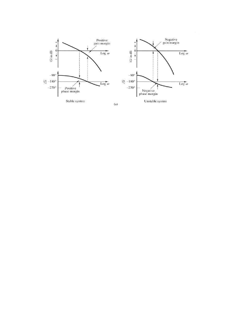
20
Figure 3-4: Gain and Phase margin base on the bode diagram [12, p.546]
21
Chapter 4
Implementation
This chapter will divided into the four stages to explain on the design approach for the
Switch Mode Multilevel Class D Power Amplifier. They are input stage, PWM stage,
H-bridge driver circuit and H-bridge operation and Output Filter stage. The main
schematic diagrams and PCB layout for the design are presented in Appendix A.
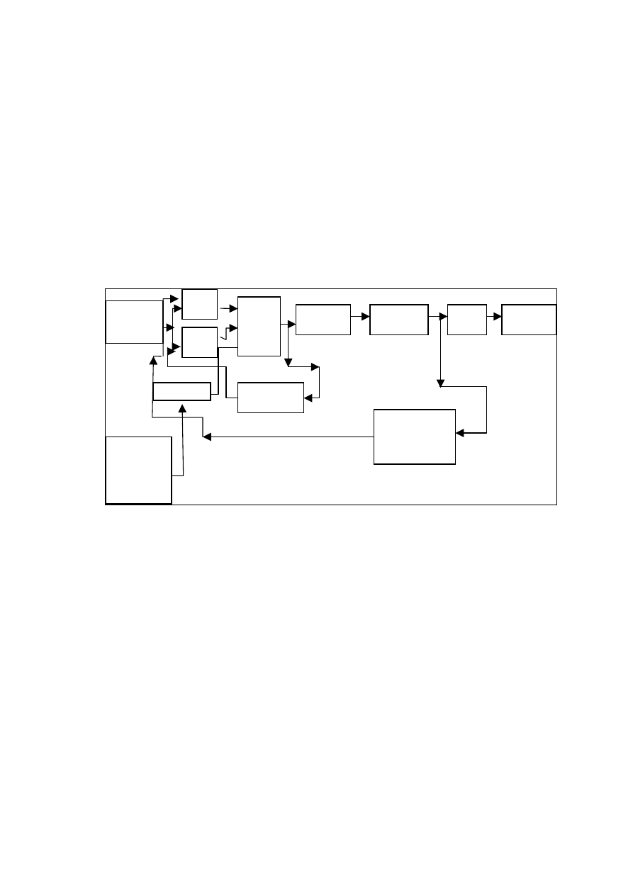
The following is the block diagram for the design.
Figure 4-1: Block Diagram for the Class D amplifier Design with close loop system
4.1 Input Stage
In the input stage there consist of the pre-amp and input low pass filter stage as well as
the carrier generation stage.
4.1.1 Carrier Generation
A driving signal (switching signal) is required to be generated in order to drive or
switch the Power MOSFET, which in this case are treat as a switch (in other word, a
PWM waveform). To generate the PWM waveform, the input audio signal will be
compared to a fixed frequency (and fixed shape) waveform. According to section 3.2
the generate pulse-train will then b used to drive the gate of the MOSFET A saw-tooth
waveform will be the most suitable carrier waveform to perform the comparison with
Analogue
input
signal
Oscillator
thru’
frequency
divider cct
(D flip flop)
integrator
MOSFET
Driver
PWM
H-bridge
MOSFET
RC low pass
Filter
Lead lag
compensator (or
low pass filter
2
nd
order)
Error
Amp.
Error
amp.
Outpu
t filter
Load
(speaker)
Outer loop
Inner loop

22
the input signal. However, it is not that simple to generate a saw-tooth waveform.
Hence, a carrier frequency with a triangular shape will be the 2
nd
best choice since a
triangular waveform will have the closest similarity to the saw-tooth waveform and
easy to generate. Another important element in the design consideration is selecting the
operating frequency or carrier frequency for the operation. The criterions on selecting
the carrier frequency have to weigh the advantages of high carrier frequency against
increased switching losses and the increased in radiated EMI/RFI (Electro Magnetic
Interference / Radio Frequency Interference). In other word, it is based on the trade off
between the power efficiency and high fidelity of the amplifier design. Since
minimizing the carrier frequency will reduce the switching losses, while maximizing
the carrier frequency will ease the design requirement for the output filter stage. From
experience from other Class D amplifier designer as well as the recommendation from
the National semiconductor LM4651 Class D amplifier data sheet’s [1] application
section, a range between 125 KHz ~ 145 KHz carrier frequency will the suitable
frequencies range for the above mentioned trade-off. Thus 125 KHz was chosen as the
carrier frequency for the design. Since it is the lowest frequency could be removed from
the PWM spectrum without causing any pass band distortion.
After selecting the carrier frequency, a circuit must be design to accomplish the
frequency generation task. Since a consistency playing a major role in generating the
carrier frequency thus a crystal oscillator will be the best choice. A 1 MHz crystal
oscillator will be used to produce a 50% duty cycle square waveform through the
implement of the following CMOS circuitry, Pierce crystal oscillator circuit [17, p.4-
25~26].
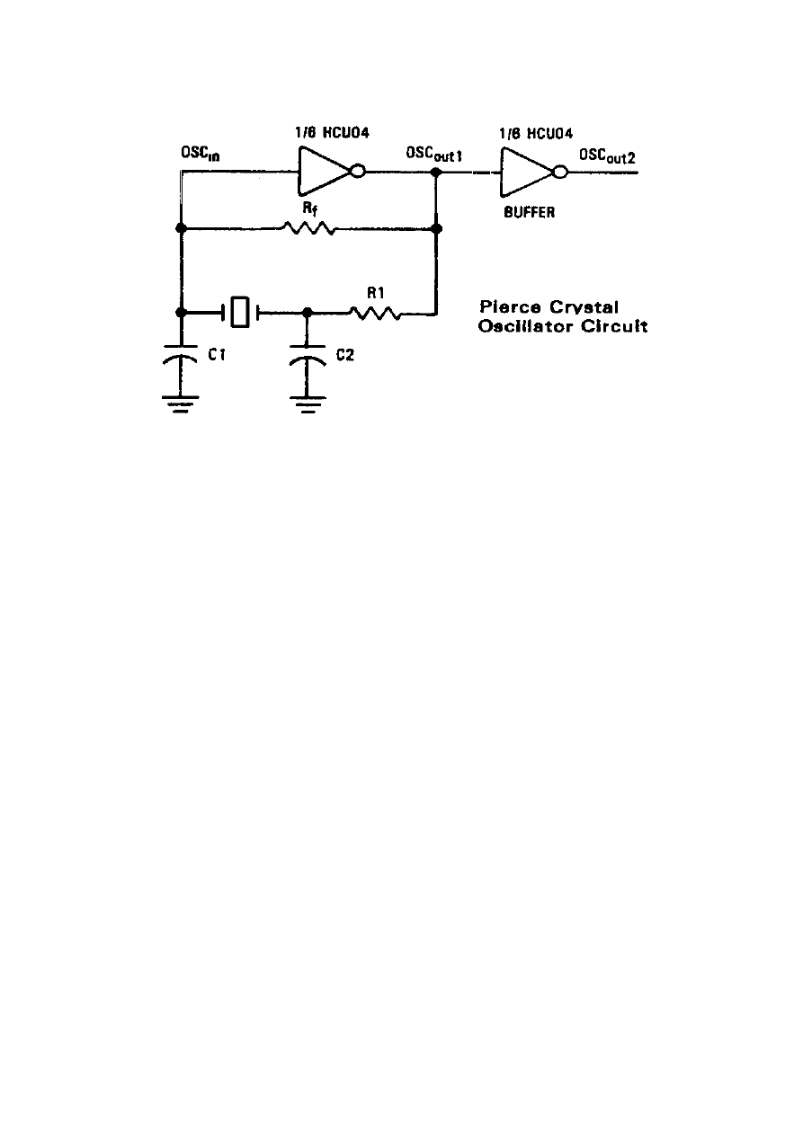
23
Figure 4-2: 1MHz Clock pulse generating circuit from a crystal [17, 4-25]
The selection for the capacitor C1 and C2 is based on the crystal oscillator performance.
The resistor R
1,
limits the drive level to keep the oscillator from overdriving, and the
crystal oscillator start-up is also proportional to the value of R
1.
[17, p. 4-25]. While for
R
f
, the feed back resistor typically ranges up to 20MΩ. It must be large enough to
prevent the phase of the feedback network from being affected in the appreciable
manner.
Yet, 1MHz clock pulse with 50% duty cycle has to be subsequently stepped down to
125 KHz for the design (Class D amplifier). This can be achieved through the used of
frequency divider circuit, which make up by numbers of D Flip-Flops. Since a D Flip-
Flop is capable to half an input frequency thus by cascading 3 of them in series, it is
able to produce a of the 125 KHz carrier frequency from a 1MHz crystal oscillator.
Here the frequency divider circuit was shown in figure 4-2.
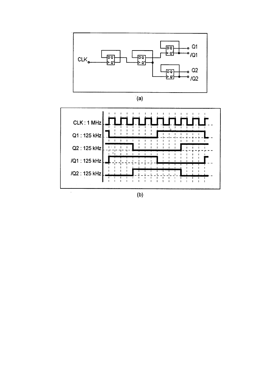
24
Figure 4-3: Frequency Divider circuit (a) and the timing diagram (b) [4]
As the figure shown the 2
nd
last D flip-flop outputs (both inverting and non-inverting)
were fed into the last D Flip-Flop in order to perform an equally space (by 90û) clock
pulses. Since a 5 level Class D amplifier is to be designed, there must be 4 carrier
waveforms to suit the interleaving techniques. These 4 equally space (90û phase shifted)
carrier waveform was generated from the frequency divider circuit both the inverting
and non-inverting output from the final stage flip-flop.
These carrier waveforms is then integrated into four 90û-phase shifted triangular
waveform through the implementation of 4 common integrator circuits. The following
figure (figure 4-3) has shown a common op-amp integrator to perform the integration.
25
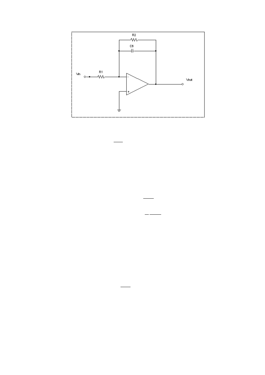
Figure 4-4: Common Integrator circuit by using an OP-Amp
∫
−
=
t
in
out
dt
v
C
R
v
0
1
1
Equation
4-1
Equation 4-1 shows the mathematical way to design the integrator circuit. Deriving
from the equation we can determine the proper components size to implement for the
design.
out
in
v
t
v
C
R
∆
∆
=
1
pp
tri
in
v
T
v
,
1
2
−
=
Equation
4-2
Arbitrary selecting the amplitude of the triangular waveform to 5 volt peak-to-peak and
R
1
= 1 KΩ, we can derive the capacitance value based on equation 4-2. Where the
capacitance of C = 2nF, choosing the preferred value C = 2n2F.
In order to ensure a bounded DC gains, resistor R
2
was included and will create a 1
st
order low pass filter with the cut frequency (ω
o
) equal to [4]:
C
R
w
o
2
1
=
Equation
4-3
This frequency must be less than the 125 KHz to allow integration of the square wave
to be proceeded. Hence, with ω
o
= 12.5 KHz (one decade less than the switching
frequency), R
2
= 27Kohm. That will conclude the carrier generation design

26
4.1.2 Input Pre-amplifier and Subwoofer filter stage
Since this Class D amplifier is designed to suit for the subwoofer application (low
frequency audio application), a pre-amplifier with a gain and a low pass filter stage is
implemented. This stage can be implemented by using a National’s dual audio
operational amplifier LM833 to perform the task [1]. The circuit is shown as figure 4-4.
Figure 4-5: The input Low Pass Filter and Pre-Amp stage circuit [1]
The 1
st
op-amp act as a 2
nd
order low pass filter while the 2
nd
op-amp is just providing a
pure gain for the input signal. In order to have a clean sounding subwoofer the filter
must be at least a 2
nd
order filter to sharply roll off the high frequency audio signals. For
a subwoofer application, the pole of the low pass filter should be around 60~180 KHz.
Hence the component values for the R and C in figure 4-4 are based on the following
Equation 4-3.
2
,
2
2
1
2
1
C
C
R
f
C
o
=
=
π
Equation 4-4
Where R
1
= R
2
= R, arbitrary taking R = 2.7 KΩ we can figure out capacitance for C
1
=
4.7µF while C
2
= 2.35 µF, choosing the closest value C
2
= 2.2 µF.
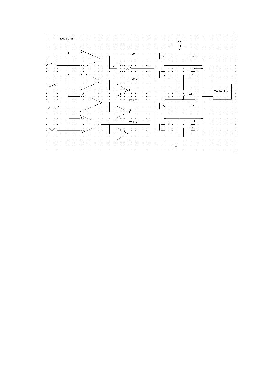
4.2 Pulse Width Modulation (PWM) Stage
A high-speed comparator is needed to perform the Pulse-Width-Modulation technique.
National Semiconductor such as LM319 and LM361 can be used for this application
due to their high-speed nature (around 80µs response time). However, LM361 is chosen
over LM319 since it have a differential outputs which make it the best companion with
the HIP4082 H-bridge MOSFET driver. Furthermore, LM361 comparator response
time is faster, 20ns, when compare to LM319 that is only 80ns. As mention before the
differential outputs, inverting and non-inverting pulsed waveform will be resulted from
the chip. These outputs will be used to feed into the driver chip to generate the driving
signal to drive the H-bridge MOSFET. A drawback is that with a 14 pin DIP chip, it is
only a single comparator package. The input audio signal and the four 90-phase shifted
triangular carrier frequency will be compared to generate the switching waveform.
There no external circuitry or components are need for this IC chip, just the power

27
supply voltage (5V) for the chip, V
+
and V
-
.
In order to generate four 90û-Phase shifted
PWM waveforms, four of this LM361 high-speed differential comparator will be used.
4.3 Inner Loop (close loop control for the PWM)
In order to reduce the non-linearity characteristic of the PWM stage, the output of the
switching frequencies are fed back to compare with the input signal. The inverting and
non-inverting (differential) outputs from the PWM stage are summed and pass through
a simple RC low pass filter to recover the audio signal (a sine waveform) from the
pulsed waveform. As in the modulated audio signal the fundamental frequency can be
extract out from its carrier frequency if the carrier frequency is more than 5 times larger
than the original signal. This will be depended on the corner frequency of the 1
st
order
RC low pass filter. The transfer Function of the RC low pass filter is stated in Equation
4- 5.
RC
s
RC
s
H
1
1
)
(
+
=
;
Equation 4-5
And
c
o
f
π
ω
2
=
;
Where
o
ω
is the cut off (corner frequency), which can be determined by Equation 4-6.
Thus,
RC
f
c
π
2
1
=
; Equation 4-6
Since the audio frequency are ranged within 20 Hz ~20 KHz, thus setting the cut off
frequency at 25 KHz will be reasonable. Hence, applying Equation 4-6, and arbitrary
choosing R = 2.7 KΩ, found that C = 2.36nF take the closest prefer value 2.2nF.
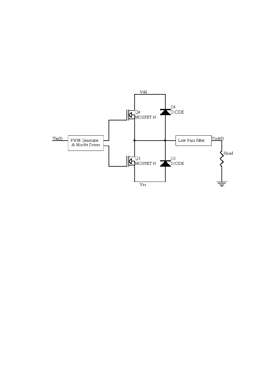
4.4 H-Bridge MOSFET and H-bridge MOSFET driver circuit
This is the heart of the Class D amplifier design, as it is produce the gain for the
amplifying process. In the design, the 4 MOSFET will be arranged in ‘H’ figure where
the load is in the center providing a bridged output. Here is the basic topology of the H-
bridge design circuit diagram.
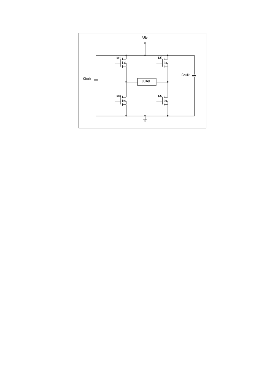
28
Figure 4-6: H-Bridge MOSFET topology
An H-bridge configuration is chosen over a half bridge configuration, as with an H-
bridge (Full-bridge configuration) it needs only a single voltage to produce alternates
polarity between +V and –V in the output. While in a half-bridge configuration a
bipolar voltage supply is needed. The H-bridge circuit operation is similar to that of the
half-bridge design, except the full-bridge design uses four MOSFETs instead of two,
uses a differential low pass filter in the feedback network to support the floating load,
and requires a second order low pass filters to attenuate the carrier frequency. The
selection of the MOSFET was base on the following criteria: peak voltage and current
requirements, body-diode reverse-recovery time, switching losses and conduction
losses. With the requirement on the peak voltage and current, the rating will determine
the rating that the MOSFET able to sustain [6].
4.5 Center Tapped Transformer for multiple outputs
The outputs from the 2 H-bridge configurations will be coupled through the use of 2
center-tapped transformers and the resulted outputs will be fed into the output filter
stage. The center –tapped transformer performance couple the output in the following
situation. When the outputs from the H-bridge MOSFET were both high (12V), the
output to from the transformer will stay at high. The output of the transformer will be
stay at low, if the H-bridge outputs are both low (0V). While the outputs from the
output were different, it will result the transformer stay in the middle position, which is
V/2. A ferrite core ETD29 was used in this thesis for the center-tapped transformer. The
winding of the transformer was design base on the following equation [10].
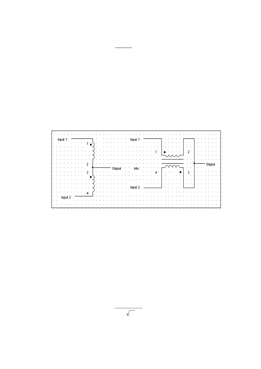
29
s
c
d
f
A
N
V
B
1
max
4
=
Equation
4-7
Where V
d
is supply voltage, N is the primary winding and Ac is the cross section area
of the core and f
s
is the switching frequency. With the B
max
= 0.2 Telsa, the N
1
= 4
turns.
In order to prevent the ETD29 ferrite core [11] being saturated, N
1
winding is increase
to 15 turns and two winding was wound in parallel, where the turn ratio is 1. The pin
out on the Bobbin (ferrite core holder) has to be carefully indicated for a center–tapped
transformer. Derivation of the pin lay out can be based on the following diagram.
Figure 4-7: Derivation on transformer Bobbin pin out
4.6 Output Filter stage
A Butterworth approximation low pass filter configuration was employed here. It was
chosen as it provides flat response in the pass band, which is critical for the audio
system to improve its dynamic performance. Furthermore less numbers of parts will be
needed. The design of this Class D amplifier will required a balanced filter since a
bridge output is expected. As a result, the design on the LC filter will be based on a
single ended approach. The transfer function for a second order Butterworth
approximation is:
1
2
2
1
)
(
+
+
=
s
s
s
H
Equation 4-8
Here the LC Low Pass Filter Half-Circuit Model
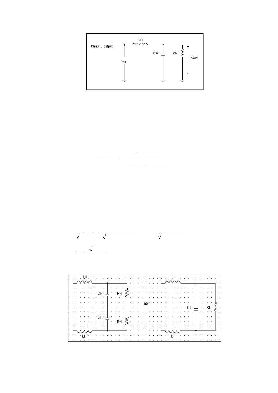
30
Figure 4-8: LC low Pass Filter half-circuit model
Realizing and deriving the transfer function of the LC filter will be based on a single
ended approach, which is modeling the bridge output LC circuit into a half circuit
model. With this half model circuit, the transfer function of the output filter can be
formed to the following equation.
H
H
H
H
H
H
in
o
C
L
s
C
R
s
C
L
s
V
s
V
s
H
⋅
+
⋅
+
⋅
=
=
1
1
1
)
(
)
(
)
(
2
Equation
4-9
The inductor and capacitor was converted into s-domain representation (L = Ls, C =
1/Cs). Equating Equation 4-8 and Equation 4-9, the value of the half model inductor
and capacitor can be determined with the following equations and easily convert them
into full model.
L
H
c
H
H
fcR
CL
R
f
R
C
⋅
⋅
=
→
⋅
⋅
⋅
=
⋅
=
π
π
2
2
1
2
2
1
2
1
Equation
4-10
H
c
H
H
H
L
L
f
R
C
L
=
→
⋅
⋅
⋅
=
=
π
2
2
1
Equation
4-11
Combination of the two half model to have the final LC Low Pass Filter.
Figure 4-9: Combination of two Half-Circuit Models

31
The inductor value remains the same for half bridge and Full-bridge, as there are two
inductors in both models. As for the cut off frequency for the LC filter,
L
c
LC
f
⋅
⋅
⋅
=
2
2
1
π
Equation
4-12
Two capacitors can be included as a high frequency by pass capacitor in the design and
they can be empirically chosen to be approximately 10% of 2 load capacitors. After
arbitrary chosen a 100uH inductor, we can easily find the value for the capacitors.
Applied Equation 4-10 and 4-11, C
L
= 5uF while the two by pass capacitor will be 1uF.
These ends the output filter design process.
4.7 Overall Close loop design
The overall close loop design for the design is referenced from the National LM4651 &
Lm4652 Overure
TM
Class D Audio Power Amplifier application circuit [1]. The
feedback is taken directly from switching outputs before the demodulating LC filter to
avoid the phase shift caused by the output filter stage. The switching frequency and its
harmonics of the feedback signal will be filtered through the RC low pass filter and a
high input impedance instrumentation amplifier will be employed to derive the true
feedback signal from the differential output, which aids in improving the system
performance.
An error amplifier will then sum this true feedback with the input signal and compare
with a zero signal i.e. to compensate the differences between the feedback and the input
signal. In this error inverting gain of this error amplifier with be set by the input
resistance R
in
and the feedback resistor R
f.
While the parallel RC low pass filter will
limit the content of input audio signal and the feedback signal. The poles of the filter is
set by the following Equation 4-13
f
f
ip
C
R
f
π
2
1
=
Equation 4-13
Here the circuit for the feedback and error amplifier circuit.
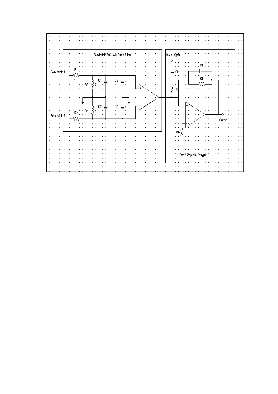
32
Figure 4-10: Feedback and error amplifier (error compensate) circuit

33
Chapter 5
Design Result and Discussion
Unfortunately, the design doesn’t work as expected while this Thesis report was written
up. This was due to the fact that the driving signal to the H-bridge MOSFET
configuration failed to give any sensible results. Even though, part of the circuitry work
as expected, yet they are only part of the main design. These circuitries are only the
support circuit for the main design. It is the Class D amplifier stage was the main
important of the entire amplifier design. If the PWM stage and the H-bridge fail to
produce any results, the power amplifier design will be a total failure. Since the output
filter stage can’t be tested without any sensible output from the H-bridge and the close
loop design can’t be examine, which is also depend on the H-bridge output. As a result
the overall performance of the amplifier design can’t be determined on those
unreasonable results. For those workable stages, the testing results (output) will be
shown respectively in this chapter. These include the input filter stage, carrier frequency
generation stage and PWM stage. While for the trouble shooting on the causes of the
failure to the design is still in the progress with the help from my thesis supervisor as
well as my course mate. The trouble shooting area will be mainly on the HIP4082 H-
bridge MOSFET drive chip as well as the H-Bridge configuration itself. The progress
will be carried on till the demo day in order to show some reasonable result on that day.
5.1 Result on the Carrier generation stage
In this stage, it will consist two main parts. They are the 125 KHz clock pulse
generation part and the triangular carrier frequency waveform generated from the
specific 1MHz clock pulse. The following results (waveform from TDS210S
oscilloscope through the WaveStar software) will show the 1MHz clock pulse generates
from the crystal oscillator and the frequency divider circuit output.
34
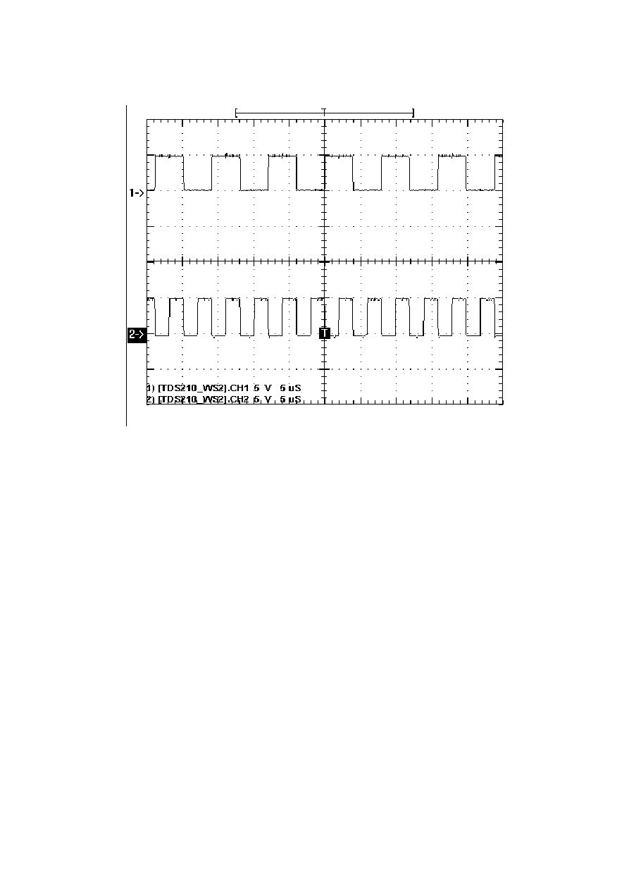
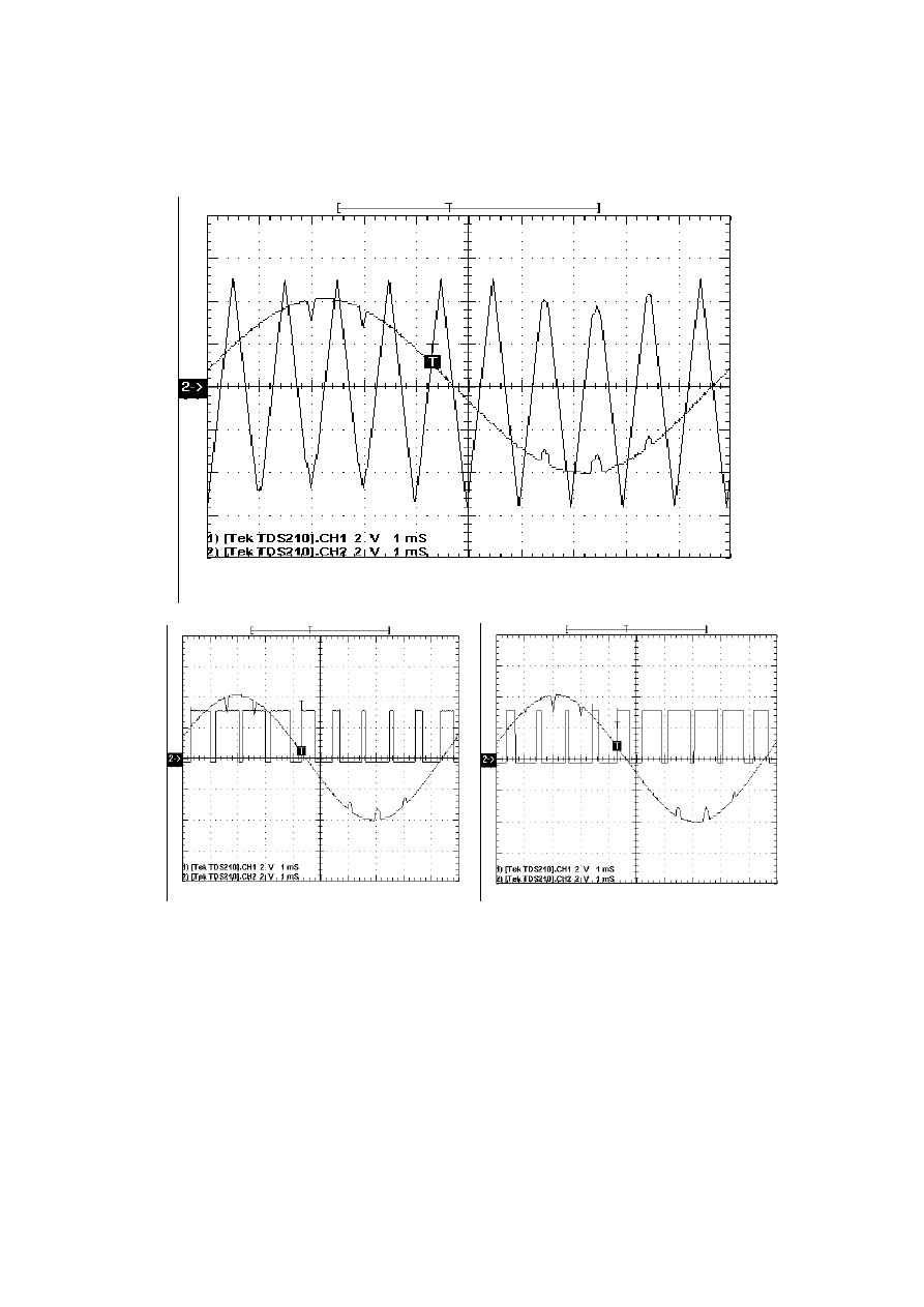
Figure 5-1: Output from Frequency divider circuit (1) 125 KHz and (2) 500 KHz
square waveform generate from 1MHz
The result shown above was base on the input of a 1MHz square waveform go through
the 3 cascaded D Flip-Flop set up as the Frequency divider circuit. The time frame
division is set to 5µs, where 125 KHz waveform take only 8µs for a cycle and 500 KHz
take only 2µs per cycle.
35
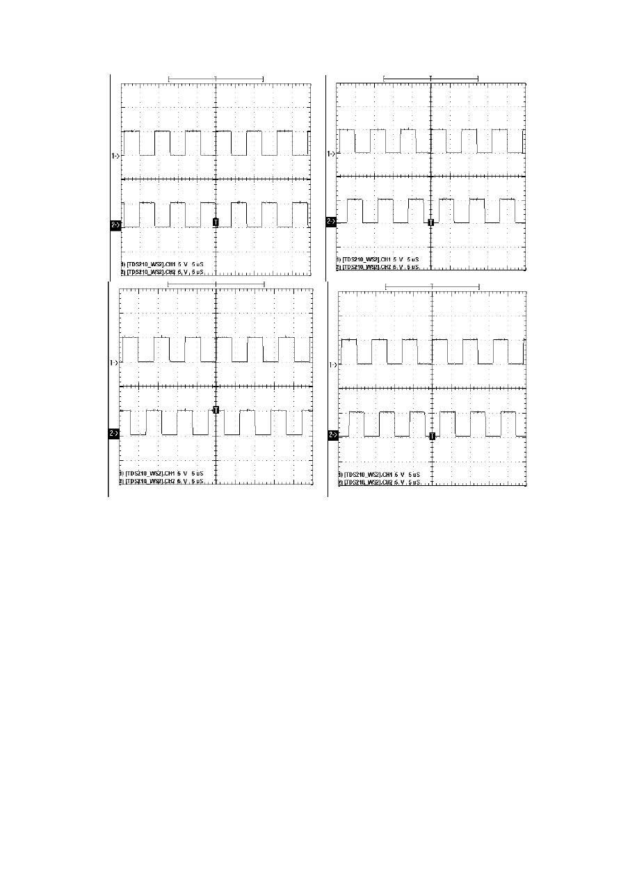
Figure 5-2: The 125 KHz square waveform (clock pulse) generate through the use
of Frequency divider circuit. Four 90û-phase shifted square waveform.
Due to the Oscilloscope won’t be able to show all the four waveforms, the waveform
was shown with one fixed clock pulse compare to the rest. Notice that they did shifted
by 90û. From the result shown above, the generation for four 90û-phase shifted square
waveform had been successfully generated. The following section will shown the result
on the respective square waveform being integrated into their respective triangular
waveform for PWM stage.
36
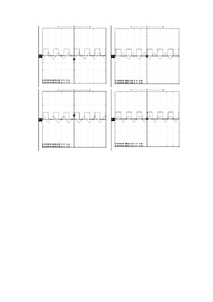
Figure 5-3: The Triangular waveform integrated from the four 90û-phase shifted
125 KHz square waveforms.
Again the maximum possible waveforms can be shown in the Oscilloscope is just 2 at a
time and due to the fact that the waveforms will be the same if taken at individual
attempt. Furthermore, a reference is needed in order to show the phase shifted triangular
waveform. From the shown results, it is obvious that LM6361 High speed Op-amp
manages to integrate the phase-shifted square waveforms into 5V
p-p
triangular
waveforms respectively. These waveforms will be used for the PWM stage.
5.2 Result from the PWM stage
The result shown as below is just a comparison on 5V
p-p
Triangular waveform (@ 1
KHz switching frequency) with a 5V
p-p
sine waveform signal (@100Hz Frequency).
That was done to show ‘visible’ PWM waveform generated. If the actual PWM is done
due to the variation in the frequency difference the result won’t be as clear as the
following result. Yet, the application of the PWM is still operate the same way. The
Switching Frequency is 125 KHz and input signal is ranged around 60~200Hz for the
37
actual design, which the input signal will more look like a constant voltage to the carrier
frequency.
(a)
(b)
(c)
Figure 5-4: Generation of PWM waveform on a 100Hz input signal with a 1KHz
triangular waveform. (a) Both input signal and Carrier frequency (b) The
non-inverting output from LM361 (c) The inverting output from LM361
5.3 The possible failure stage
These will be purely based on assumption/estimation, as the trouble shooting is still on
the way. Even though the driving signal had been fed into the gate of the MOSFETs,
the outputs from the H-Bridge weren’t in any similar to the expected outcome. The
supply voltage can only supply at ±8 V even though it was set to ±12V initially. This

38
was due to the voltage supply unit was current limited at 3 Ampere (the Circuit design
was drawing more than 3 Ampere).
5.3.1 H-Bridge MOSFET driver chip (
HIP4082
) and H-bridge
configuration
The testing on the PCB board was still carry on by turning on the power supply just for
a little while to check on the output from the H-bridge driver. Initially the test was done
without the 8 MOSFETs on the PCB. With that, the power supply unit still able to
supply a full ±12V to the circuit. However, due to the result output pins on the
HIP4082, such as AHO, BHO, ASH and BSH [refer to HIP4082 data sheet] (controlled
by the respective switching signal) wasn’t similar to the expecting results the MOSFET
was mount on to check to output. Since those pins, especially the AHO output needs to
be reference from the AHS output. Yet after mounting on the MOSFETs, the current
draw out from the unit was surge up to more than 3 Ampere, when comparing to the
circuit without MOSFET was barely 1 Ampere. As a result, testing was carried on with
voltage supply unit supplying a current limit at 1 Ampere. However, output result from
the AHO still stay at constant upper rail voltage (12V) supplied from the voltage unit.
There was nothing similar to the switching signal from the HIP4082 driver. As the
output of the H-bridge was expected to be in a similar form of the switching signal but
with alternate polarity of voltage of the VDC supplied. The output of AHO and BHO
pins stay at constant voltage (with on switching signal waveform alike), which cause
the particular MOSFET becoming very hot (can’t touch it with more than 2 seconds)
since it is in its linear region on state. With the attempts to increase the supply current,
eventually the bootstrap capacitor for the HIP4082 was smoked (Capacitor busted).
Reason for that might be the increased in the supply current. Yet, the bootstrap
capacitance was chosen to be much greater than expected value based on the following
equation:
gate
gate
EXT
V
Q
C
=
and C
boot
>> C
ext
Equation 5-1

39
Where C
boot
is the bootstrap capacitance, V
gate
is the voltage of the driving signal and
Q
gate
is the maximum charge of the MOSFET gate terminal. Trough the calculation the
value for the bootstrap capacitor is 100 times of 1.25nF that is 1.25µF. Hence, a
Tantalum 1µF was used for the application, yet it failed.
A new type of capacitor with slightly lower capacitance was used after that. However
none of the MOSFET is switching. Outputs from the MOSFET are either constantly
high (12V) or constantly Low (0V).
The following tasks will be recommended (might be or might not be the remedy to the
problem) to carry out till the demo day in order to resolve the problem:
•
Check the functionality on the MOSFET (in case some of than might ‘dead’
after that incident)
•
Review the supply current needed for the circuit design
•
Carefully check on the PCB design and connection (which had been done
couple times)
•
Connect up the LC low Pass filter (output filter stage) and the load.
•
Review the design on the H-Bridge (Since each of the MOSFET was driven
individually by each of the driving signal. Furthermore, the generated driving
signal was done through the comparison between the input signal with the
phase-shifted triangular waveforms).

40
Chapter 6
Conclusion
From the previous chapter, it can be realize that the main objective of this thesis have
been failed to achieve. During the testing for the circuit design, there contains not a
single sensible result or output to prove that the design can achieve the underlying
requirement. However, the design failure might be is based on man-make error which
can be resolve through the trouble shooting process. In other word, the theory behind
the design does prove that the performance and implementation is achievable. Through
this thesis project, it did show that the implementation on Class D audio Power
Amplifier is more complicated than the Classical Audio Amplifier. During the process,
it also provides a clear view on some particular concepts on the audio amplifier as well
as expands my knowledge on the power electronics field. Even though, this thesis
report was conclude as failed to achieve the underlying requirement, the trouble
shooting on the design will be carried on till the demo day, so that there will be some
reasonable result to back up the design theory as well as achieve the main objective of
the thesis – build a workable Switch Mode Multilevel (Class D) Power Amplifier.
6.1 Future work
Due to the failure of achieving the underlying objective of the thesis, the future work
for this thesis will be focus on “getting the Design work as expected”. That will include
designing an H-Bridge driver circuitry instead using a HIP4082 chips or look into the
problems that cause the failure of the design when using the chip. Based on the
application notes of HIP4082 it is possible to drive either a H-bridge driver or a half-
bridge configuration thus the failure of the design might be just some silly human
mistake. The other main concerns will be focus on the current issue in the circuit
design. Throughout the whole design, the current issue have been left out for no reason.
That was cause by the fact that I personally thought that when using MOSFET current
won’t be the issue for the design circuit. This, in fact causing me the failure to this
design (might be one of the main reasons).
On the other hand, there also exist a few one-chip solutions for Class D amplifier. Even
though those IC chip only provide a few watts output up to 50W, yet some of them did

41
manage to have large output power with low THD and >85% power efficiency.
However, most of them are only for portable audio system and etc. Texas Instrument
has most of the Class D amplifier IC with the output voltage range around 20W. They
even come out a filter less Class D amplifier IC chip, which worth to have a closer look
in order to implement that feature in the multilevel switch mode Class D amplifier
design in the future. Cirrus and National Semiconductor also provide a few good design
considerations on this particular area.
Another new breed of amplifier type also exists recently that is the Class T amplifier,
which has similar power efficiency (or better) than Class D amplifier and less
distortion. It has a few superior performances compare to Class D such as similar power
efficiency and less distortion produce in the output. This also provides a good research
area to improve or replace the existing Class D power amplifier design.
Finally, most of the Class D amplifier design constraint on it inherent limitation on high
frequency performance that limiting it application on subwoofer system. Research on
the area to improve this limitation on Class D amplifier nature will give the boost of
Class D amplifier in the audio amplifier market.

I
Appendix A
Schematic Diagrams
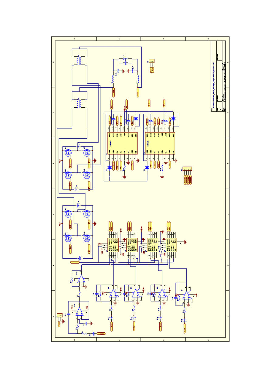
II
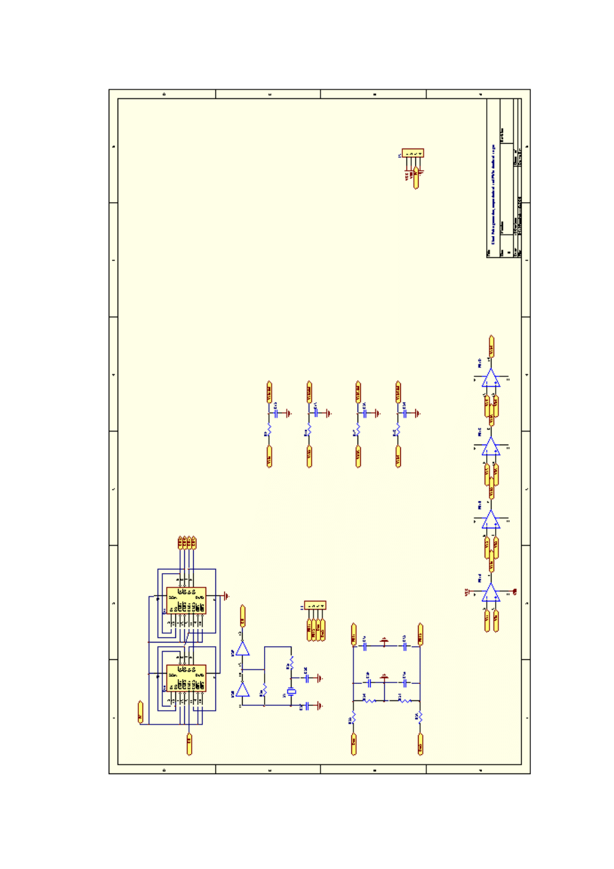
III
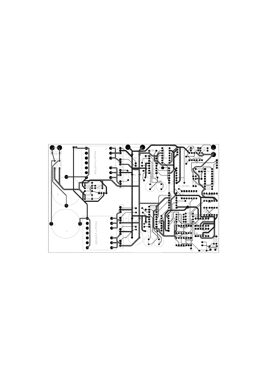
IV
Appendix B
PCB Layout
There still some connections need to be fixed up during the testing. Most of the
feedback connection was left open in order to analyze the open loop system
performance before the close loop system can be employed. Since during the testing,
the H-bridge output was not similar to expected outcome, these connections are still left
open. If the circuit failure can be resolved the close loop system will be connect up for
evaluating the overall system performance. Result will then be shown on the demo day,
if the problem can be solved.

V
Appendix C
Bibliography
[1]
National Semiconductor, Data sheet for LM4651 & LM4652 Overure
TM
Audio
Power Amplifier170W Class D Audio Amplifier Solution, http://
www.national.com/pf/LM/LM4651.html#Datasheet
, August 2000
[2]
Texas Instruments, Application report for Design Consideration for Class-D
Audio Power Amplifiers,
http://www-s.ti.com/sc/psheets/sloa031/sloa031.pdf
,
August 1999
[3]
Brain E.Attwood, “Design Parameters Important for the Optimization of Very
High-Fidelity PWM (Class D) Audio Amplifiers”, Journal of Audio
Engineering Society, vol.31, no.1, November 1983, pp.842-853
[4]
Christopher N. Hemmings, Improving Class D Audio Power Amplifiers,
University of Queensland, St Lucia, Department of Computer Science and
Electrical Engineering, 1999
[5]
Tng Chee Wan, Multilevel Switch Mode Class D Amplifier, University of
Queensland, St Lucia, Department of Electrical and Computing Engineering,
1998
[6] Jeffrey
D.Sherman,
Class D amplifier Provide high efficiency for audio system,
http://archives.e-insite.net/archives/ednmag/reg/1995/052595/11df3.htm#pic1
,
May 1995
[7] Duncan
McDonald,
Class D audio-power amplifiers: Interactive simulations
assess device and filter performance,
http://www.e-
insite.net/ednmag/index.asp?layout=article&articleId=CA60948&stt=001
, April
2001
[8] Sayed-amr
El-Hamasy,
Design of high efficiency RF Class D power amplifier,
IEEE transaction on power electronics, vol.9 no.3, 1994, pp.298-301

VI
[9]
Brett A.Miwa, David M.Otten and Martin F.Schlecht, “High Efficiency Power
Factor Correction using Interleaving Techniques”, APEC’92, IEEE, USA, 1992,
pp.557-68
[10] Ned Mohan, Tore M. Underland and William P.Robbins, Power Electronics:
Converter, Application and Design, Second Edition, John Wiley & Son Inc.,
USA 1995
[11] Robert
W.
Erickson,
Fundamentals of Power Electronics, Kluwer Academic
Publishers. Massachusetts, 1999
[12] Katsuhiko
Ogata,
Modern Control Engineering, Third Edition, Prentice-Hall
Inc., New Jersey, 1997
[13] Jerry C. Whitaker, The Electronics HandBook, Technical Press Inc., Boca
Raton, Fla. : CRC Press in cooperation with IEEE Press, 1996, chapter: Solid-
State Amplifier - Class D voltage Switch-Mode Amplifier, pp.545-549
[14] Norman S. Nise, Control System Engineering, Third Edition, John Wiley & Son
Inc., New York, 2000
[15] Allan R. Hambley, A Top-Down Approach to Computer-Aided Circuit Design,
Prentice Hall Inc. New Jersey, 1994
[16] Harris Semiconductor, Data sheet for HIP4082 H-Bridge FET driver,
http://www.farnell.com/datasheets/4477.pdf
, March 1995
[17] Motorola
semiconductor,
Motorola High Speed CMOS Logic Data
[18] Elliot
Cohen,
The Audio Advisor,
http://eli47.tripod.com/Page2.html
[19] National Semiconductor, Data Sheet for LM361 High Speed Differential
Comparator,
http://www.national.com/ds/LM/LM161.pdf
, August 2000
Wyszukiwarka
Podobne podstrony:
AMP E 323
HF 91110 80 Amp Inverter Arc Welder
sci&, Studia, I rok, I rok, II semestr, Chemia II
cewka& kondenstaror
Cykliczny AMP
High Power Car Stereo Amp
Bose AM3 amp
Stany szczegT lnego zagro&not;enia, STANY SZCZEGÓLNEGO ZAGROŻENIA
NAJWAŻNIEJSZE KOLONIE & DEKOLONIZACJA
Asertywno&
Onkyo ASV610PRO AMP
AMP 5 Levels of Conversation
amp
Technologia Âciekˇw 1100 n, Inżynieria środowiska, Inżynieria środowiska 1, Technologia wody i ściek
PD- Lab 1-2 Prolog i SWI& 39, Informatyka
DB Systems Super High Grade Pre amp and DB 4 Moving Coil Cartridge Pre Amp
więcej podobnych podstron