
972
Service Manual

1
TABLE OF CONTENTS
SERVICE WARNING
··········································································
2
A. IMPORTANT SAFETY INSTRUCTION
···········································
2
B. INSTALLATION
···············································································
3
C. CONTROL LOCATION
·····································································
4
D. OPERATION Direct
–
–
A
A
c
c
c
c
e
e
s
s
s
s
F
F
e
e
a
a
t
t
u
u
r
r
e
e
s
s
···········································
5
E. SPECIFICATIONS
···········································································
7
F. TIMING CHART
···············································································
8
G. CONDUCTION VIEW
·····································································
10
H. ADJUSTMENT PROCEDURE
························································
13
I. TROUBLE SHOOTING HINTS
························································
14
J. REPLACEMENT PARTS LIST
························································
18
K. BLOCK DIAGRAM
·········································································
22
L. SCHEMATIC DIAGRAM
·································································
23

2
WARNING
To prevent from fire or shock hazard,do not expose monitor to any rain or any form of water.High voltage is
inside the monitor so please do not remove the back cover of the cabinet if you are not a qualified monitor
engineer.Contact the local dealer or the nearest Proview branch office if you need help.
A. IMPORTANT SAFETY INSTRUCTION
Prior to using this service manual,please ensure that you have carefully followed all the procedures outlined in
the user's manual for this product.
1.
Read all of these instructions.
2.
Save these instructions.
3.
Follow all warnings and instructions a marked on the product.
4.
Unplug this product from the wall outlet before cleaning.Do not use liquid cleaners or aerosol
cleaners, use a damp cloth for cleaning.
5.
Do not use this product near water.
6.
Do not place this product on an unstable cart,stand or tablle.The product may fall,causing serious
damage to the product.
7.
Slots and openings in the cabinet and the back or bottom are provided for ventilation,to ensure
reliable operation of the product and to protect it from overheating,those openings must not be
blocked or covered.The openings should never be blocked by placing the product on a bed,sofa, rug,
or other similar surface.This product should not be placed in a built-in installation less proper
ventilation is provided.
8.
This products should be operated from the type of power source indicated on the marketin label.
If you are not sure of the type of power available, consult your dealer or local power company
9.
This product is equipped with a 3-wire grounding type plug,a plug having a third (grounding)
pin.This plug will only fit into a grounding-type power outlet.This is a safety feature,if you are
unable to insert the plug into the outlet,contact your electrician to replace your obsolete outlet.Do
not defeat the purpose of the grounding-type plug.
10.
Do not allow anything to rest on the power cord.Do not locate this product where persons will walk
on the cord.
11.
If an extension cord is used with this product,make sure that the total of the ampere ratings on the
product plugged into the extension cord to the waplugged into outlet does not exceed 15 ampere.
12.
Never push objects of any kind into this product through cabinet slots as they may touch dangerous
voltage points or short out parts that could result in a risk of fire or electric shock.Never spill liquid
of any kind on the product.
13.
Do not attempt to service this product yourself,as opening or removing covers may expose you to
dangerous voltage points or other risks.Refer all servicing to service personnel.
14.
Unplug this product from the wall outlet and refer servicing to qualified service personnel under the
following conditions.
a.
When the power cord or plug is damaged or frayed.
b.
If liquid has been spilled into the product.
c.
If the product has been exposed to rain or water.
d.
If the product does not operate normally,when the operating instructions are followed.Adjust
only those controls that are covered by the operating instructions since improper adjustment of
other controls may result in damage and will often require extension work by a qualified
technician to restore the product to normal operation.
e.
If the product has been dropped or the cabinet has been damaged.
f.
If the product exhibits a distinct change in performance,indicating a need for service.
3
B. Installation
B-1 Connect your monitor to computer
1 Turn off your computer and unplug its power cable.
2 Connect the signal cable to the video port on the back of your computer.
3 Connect the power cable for your monitor to the DC adapter and connect to the adapter the DC power jack
on the back of your monitor.
Note : You must use the supplied power adapter.
4 Speaker connect one end of the audio cable to the connector on the back of the monitor AUDIO IN, and
the other end to the sound card of the computer LINE OUT .
5 Plug the computer and monitor power cables into a nearby outlet.
6 Turn your computer and monitor on, if your monitor display an image, you have successfully installed the
monitor. If the monitor does not display an image, check all the connections and repeat steps 1-5 above.
Connecting the monitor to the computer and the power supply
4
C. CONTROL LOCATION
Font control panel
1. Menu Button 4. Power Button
2. Select Button 5. LED (Power Display)
3. Auto Button
Rear panel
1. VGA Signal Cable
2. Power jack
3. Line in jack
5
D
D
.
.
O
O
P
P
E
E
R
R
A
A
T
T
I
I
O
O
N
N
D
D
i
i
r
r
e
e
c
c
t
t
–
–
A
A
c
c
c
c
e
e
s
s
s
s
F
F
e
e
a
a
t
t
u
u
r
r
e
e
s
s
D-1 Power ON/OFF Switch
This button is used to turn the monitor ON and OFF.
NOTE :
The ON/OFF switch does not disconnect the device from the main voltage.
To completely disconnect the mains voltage, please remove the power plug from the socket.
D-2 Power indicator
This indicator lights up green when the monitor operates normally. If the monitor is in power saving mode,
this indicator change to amber when monitor is turn off, this indicator change to dark.
D-3 AUTO
Press AUTO button and release the auto adjust display mode will tune to the utmost
performance according to VGA setting.,
D-4 Volume
This feature adjust the ┼ button to increase the volume and adjust ─ button to decrease the volume.
D-5 Menu Features
The following features can all be accessed using your monitors on screen menu system.
When finished making adjustments to a feature, push the exit button to turn off the menu.
Step 1.
Press MENU Button to activate the OSD menu.
Step 2.
Press CH Button ▲ or CH Button ▼ to scroll through and highlight the main function list.
Step 3.
When the desired function is highlight, press MENU Button a second time, the sub-menu(second
page) will change to a sub-menu near main menu.
Step 4.
Press MENU Button and release again. The highlight of adjusted items and scroll bar will change
color from pink to blue.
Step 5.
To make your adjustment, press CH Button ▲ or CH Button ▼ clockwise to increase or
counterclockwise to decrease the setting.
Step 6.
Press and release MENU Button again to store the change. You can select other functions to adjust
by pressing CH Button ▲ or CH Button ▼. You can also select the EXIT icon and press MENU
Button to go back to the main menu.
Step 7.
Report step 2 through 6 to make further adjustments.
D-6 OSD menu
1. Main menu
OSD main menu of controls gives you an overview of the selection of controls available. When you want to
make adjustment of the screen image, press and release button Menu
6
2. Brightness
Adjust the overall image and background screen brightness.
3. Contrast
Adjust the image brightness in relation to the background.
4. H. Position
To move the picture image horizontally left or right.
5. V. Position
To move the picture image vertically up or down.
6. H Size
To increase or decrease the horizontal size of image.
7. Phase
To improve focus clarity an image stability.
8. Color Select
Color Select Menu
Select user mode
User color you can adjust to individual color gum intensity by yourself. Increase or decrease red, green or
blue depending upon which color is selected.
Cool
This control adjusts the color temperature of the screen image this item are preset by factory, you can not
adjust these setting. The performance is bluer and brighter.
Warm
The performance is redder ad closer to paper white.
9.Auto
Auto adjust display mode to its utmost performance according to VGA setting. In the event of the display
image needs further adjustment.
10.Reset
Reset the currently highlighted control to the factory setting. User must be using factory preset video mode
to use this function.
11. Language
You can choose one of the eight language you need.
12. OSD
You can choose where you would like OSD image to appear on your screen.
H Position :
To move the OSD image horizontally left or right.
V Position :
To move the OSD image vertically up or down.
Exit :
To exit the menu.
7
E. SPECIFICATIONS
1.
Maximum Resolution
1280 x 1024 @ 75Hz
2.
Recommend Resolution
1280 x 1024 @ 60Hz
3.
Synchronization Range
Horizontal
Vertical
31 – 80 KHz
60– 75 Hz
4.
Active Display Area
376mm (H) x 301mm (V)
5.
Dot Pitch
0.294(H) x 0.294(V) mm
6.
Support display colors
16.7M color
7.
Contrast Ratio (Typical)
600
8.
Luminance of White
250cd/m²
9.
Bandwidth
135MHz
10.
User Control
6 Key Switch
11.
OSD Function
Brightness, Conrast, H-Pos, V-Pos, H. Size, Phase,
Color Select, Auto, Reset, Language, OSD Adjust, Exit
12.
View Angle CR=5
Horizontal
Vertical
85 , 85 Degrees
85 , 85 Degrees
13.
Power Source
100 – 240 Vac 60 / 50 Hz
14.
Power Consumption
60W (max.)
15.
Connection Type
15 Pin D Type
16.
Input Signal
Video
Sync.
Analog R.G.B. , 0.7Vp-p / 75 Ohms
TTL level,positive or negative polarity
17.
Color Temperature
Cool (9300°K) / Warm (6500°K)
18.
Dimension (WxHxD) Packing
Set
525x510x155mm
438x440x177mm
19.
Monitor Weight
8.9Kg / 6.9Kg
20.
Base Operation
Tilt
0 / + 15 degree
21.
Power Saving
ON
STAND BY
OFF
<
60W
<
5W
<
5W
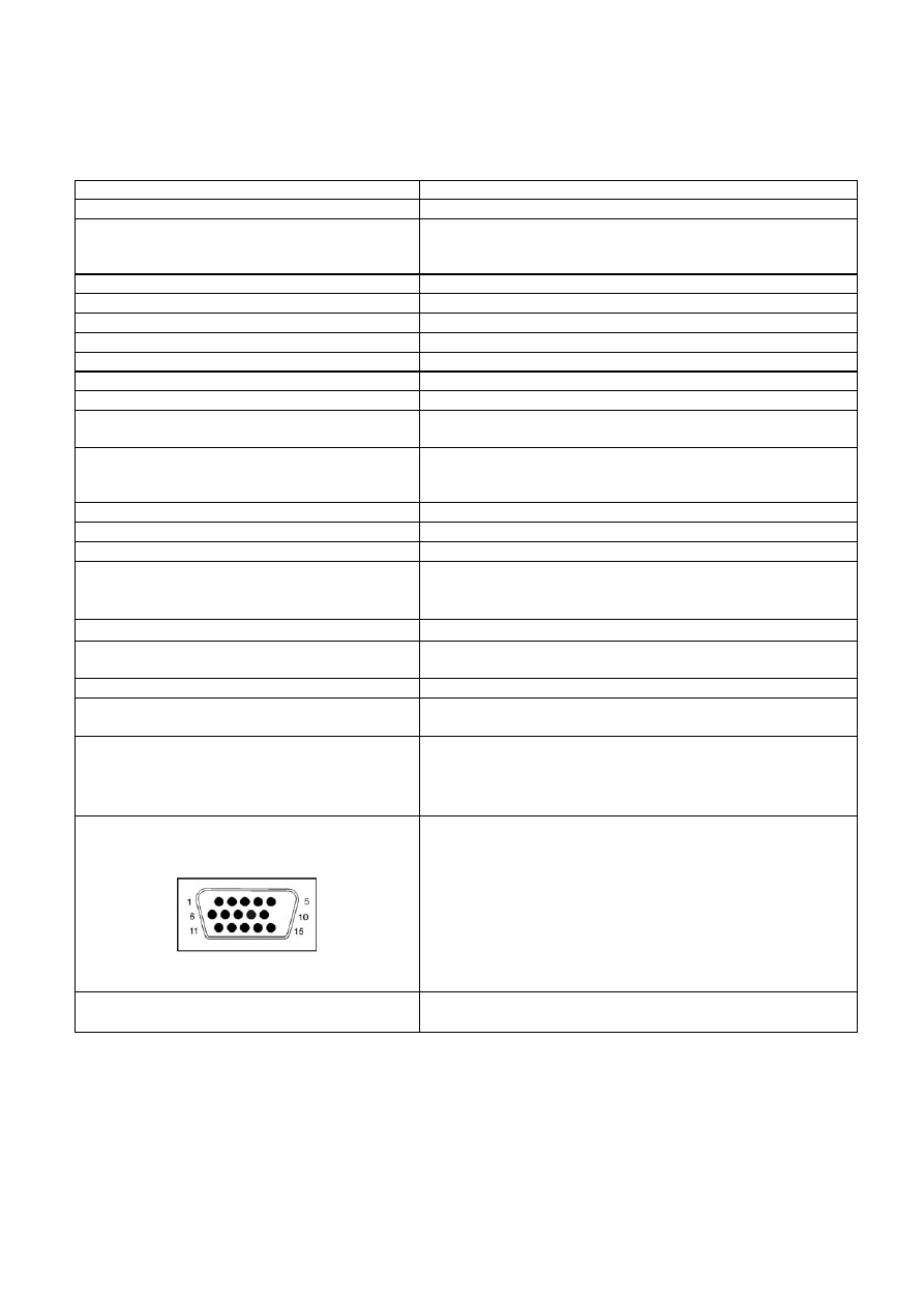
D-Sub Signal connector PIN assignment
PIN Signal
PIN Signal
1.
Red
9.
VDD from PC for DDC
2. Green
10. Sync.
Ground
3.
Blue
11.
Ground
4.
Ground
12.
SDA (For DDC)
5.
Self Test
13.
Horizontal Sync.
6.
Red Ground
14.
Vertical Sync.
7.
Green Ground
15.
SCL (For DDC)
22.
Signal Connector Pin Assignment
8.
Blue Ground
23.
Audio signal
3.5Φ stereo phone jack
2.5+2.5W 8Ω Speaker
8
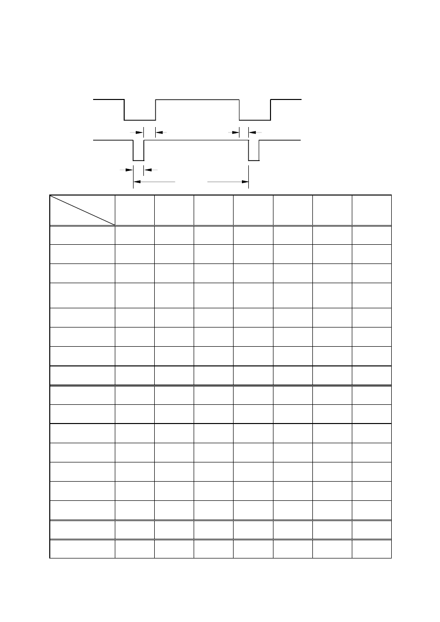
F.TIMING CHART
Video
Back porch Active display Front porch
Sync.
Sync-width
Total
Preset
Modes
VGA
720X400
VGA
640X480
VESA
640X480
VESA
640X480
VESA
800X600
VESA
800X600
VESA
800X600
Pixel clock
(MHz)
28.325 25.175 31.500 31.500 36.000 40.000 50.000
H-Frequency
(KHz)
31.472 31.469 37.861 37.500 35.156 37.879 48.077
H-Total
(
µ
s)
31.774 31.778 26.413 26.667 28.444 26.400 20.800
H-Active Display
(µs)
25.419 25.422 20.317 20.317 22.222 20.000 16.000
H-Blanking
(µs)
6.355 6.356 6.095 6.349 6.222 6.400 4.800
Front Porch
(µs)
0.635 0.636 0.762 0.508 0.667 1.000 1.120
H-Sync-width
(µs)
3.813 3.813 1.270 2.032 2.000 3.200 2.400
H-Back Porch
(µs)
1.906 1.907 4.063 3.810 3.556 2.200 1.280
V-Frequency
(Hz)
70.1 59.94 72.81 75.0 56.25 60.3 72.2
V-Total
(ms)
14.267 16.683 13.735 13.333 17.778 16.579 13.853
V-Active Display
(ms)
12.710 15.253 12.678 12.800 17.067 15.840 12.480
V-Blanking
(ms)
1.557 1.430 1.057 0.533 0.711 0.739 1.373
V-Front Porch
(ms)
0.413 0.318 0.238 0.027 0.028 0.026 0.770
V-Sync-width
(ms)
0.064 0.064 0.079 0.080 0.057 0.106 0.125
V-Back Porch
(ms)
1.080 1.049 0.740 0.427 0.626 0.607 0.478
H/V Sync. Polarity
-
+
-
-
-
-
-
-
+
+
+
+
+
+
Interlace
NONE NONE NONE NONE NONE NONE NONE
9
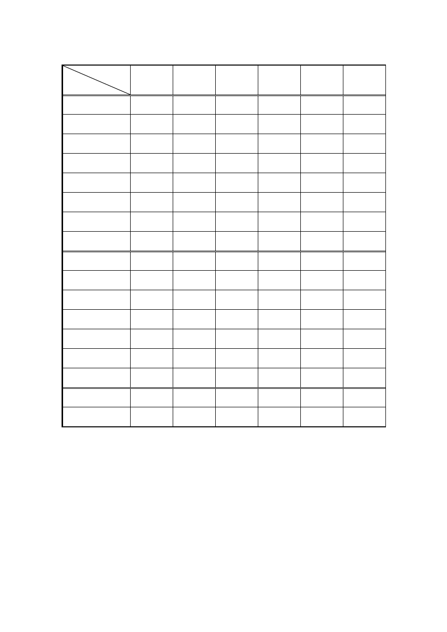
Preset
Modes
VESA
800X600
VESA
1024X768
VESA
1024X768
VESA
1024X768
VESA
1280X1024
VESA
1280X1024
Pixel clock
(MHz)
49.500 65.000 75.000 78.750 108.00 135.00
H-Frequency
(KHz)
46.875 48.363 56.476 60.023 63.981 79.976
H-Total
(µs)
21.333 20.677 17.707 16.660 15.630 12.540
H-Active Display
(µs)
16.162 15.754 13.563 13.003 11.852 9.481
H-Blanking
(µs)
5.172 4.923 4.053 3.657 3.778 3.022
Front Porch
(µs)
0.323 0.369 0.320 0.203 0.444 0.119
H-Sync-width
(µs)
1.616 2.092 1.813 1.219 1.037 1.067
H-Back Porch
(µs)
3.232 2.462 1.920 2.235 2.296 1.837
V-Frequency
(Hz)
75.0 60.0 70.1 75.0 60.0 75.0
V-Total
(ms)
13.333 16.666 14.272 13.328 16.661 13.329
V-Active Display
(ms)
12.800 15.880 13.599 12.795 16.005 12.804
V-Blanking
(ms)
0.533 0.786 0.673 0.533 0.656 0.525
V-Front Porch
(ms)
0.021 0.062 0.053 0.017 0.016 0.013
V-Sync-width
(ms)
0.064 0.124 0.106 0.050 0.047 0.038
V-Back Porch
(ms)
0.448 0.600 0.513 0.466 0.594 0.475
H/V Sync. Polarity
+
+
-
-
-
-
+
+
+
+
+
+
Interlace
NONE NONE NONE NONE NONE NONE

11
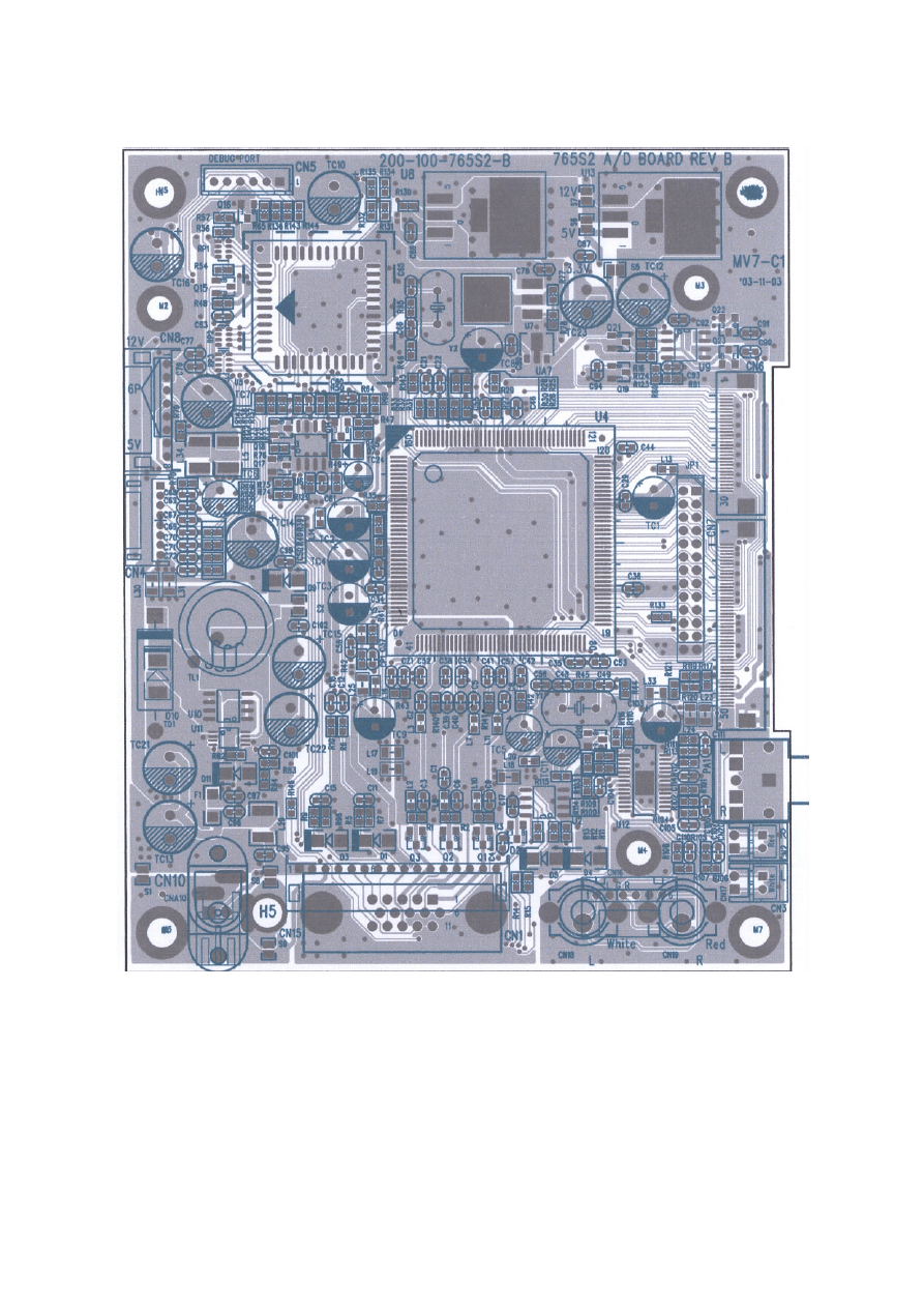
G. CONDUCTION VIEW
MAIN BOARD (Component Side)
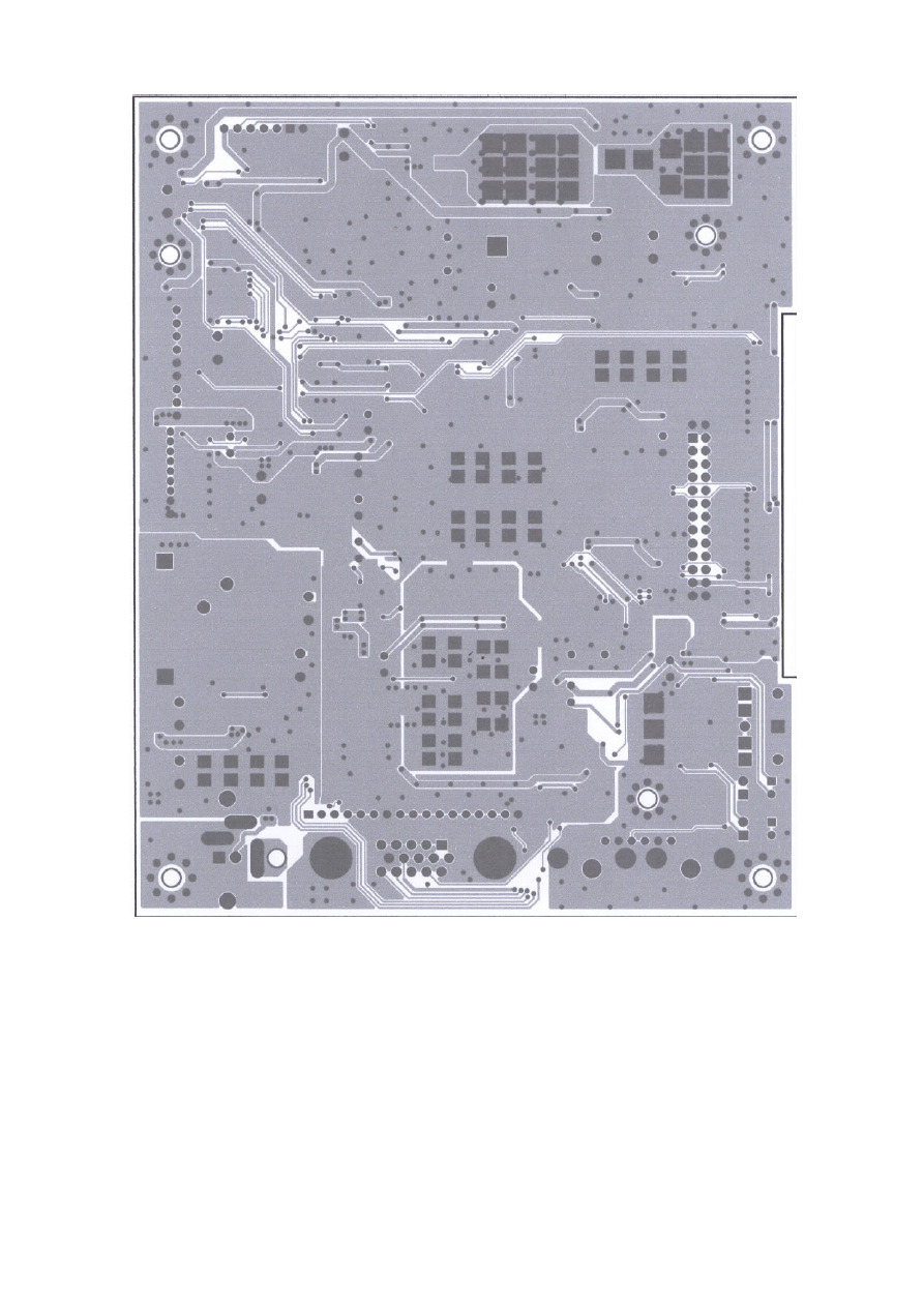
12
MAIN BOARD (Solid Side)
13
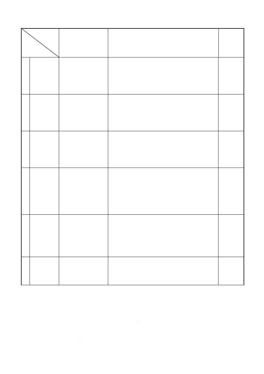
H. ADJUSTMENT PROCEDURE
ITEM
Program
Menu.
﹟Test Meter
﹡Test Point
﹫Pattern
Operation
Check
Value
A
B+
Check
﹟Digital Voltmeter
﹡CN7
﹫Crosshatch Pattern
(31.5KHz,640x480)
1.
Plug power cable into the adapter, check adapter
power indicator light up green.
2.
Make sure the voltage of the power plug (CN7)
on the main PCB to the value shown at right.
12.0V
±0.2V
B
Power Saving
Check
﹟Wattmeter
﹟PC or Pattern
generator
﹫Crosshatch Pattern
(31.5KHz,640x480)
1.
Unplug the signal cable into the monitor.
2.
Turn the power switch of the monitor ON.
3.
Check monitor power indicator light up orange.
4.
Make sure the wattmeter value shown at right.
5.
OSD will be display “NO SIGNAL” Picture.
< 2.5W
C
Into Factory
mode
﹟PC or Pattern
generator
﹫Crosshatch Pattern
(31.5KHz,640x480)
1.
Hold ‹ key,then turn the power switch of the
monitor OFF.
2.
Hold › key,then turn the power switch of the
monitor ON.
3. You can into factory adjustment mode.
D
Auto mode
Check
﹟PC or Pattern
generator
﹫Crosshatch Pattern
(1024x768/60Hz)
1.
Press and relese the MENU knob to activate the
OSD menu.
2. Move the OSD to the AUTO function,press MENU
key auto adjuat display mode to its utmost
performance according to VGA setting.
3. In the event of the display image needs further
adjustment
E
White
Balance
Adjust
﹟
PC or Pattern
generator
﹫White Pattern
(1024x768/60Hz)
1.
Move the OSD to the COLOR mode (AUTO COLOR
2.
set color is 9300
°K using the OSD,Check the value
shown at right.
Y
= 220±0.1FL x = 0.283±0.01 y = 0.297±0.01
3. set color is 6500
°K using the OSD,Check the value
shown at right.
Y = 220±0.1FL x = 0.313±0.01 y = 0.329±0.01
F
OSD
Language
Setting
﹟
PC or Pattern
generator
1.
Move the OSD to the LANGUAGE mode.
2.
You can choose one of the eight language you need.
14
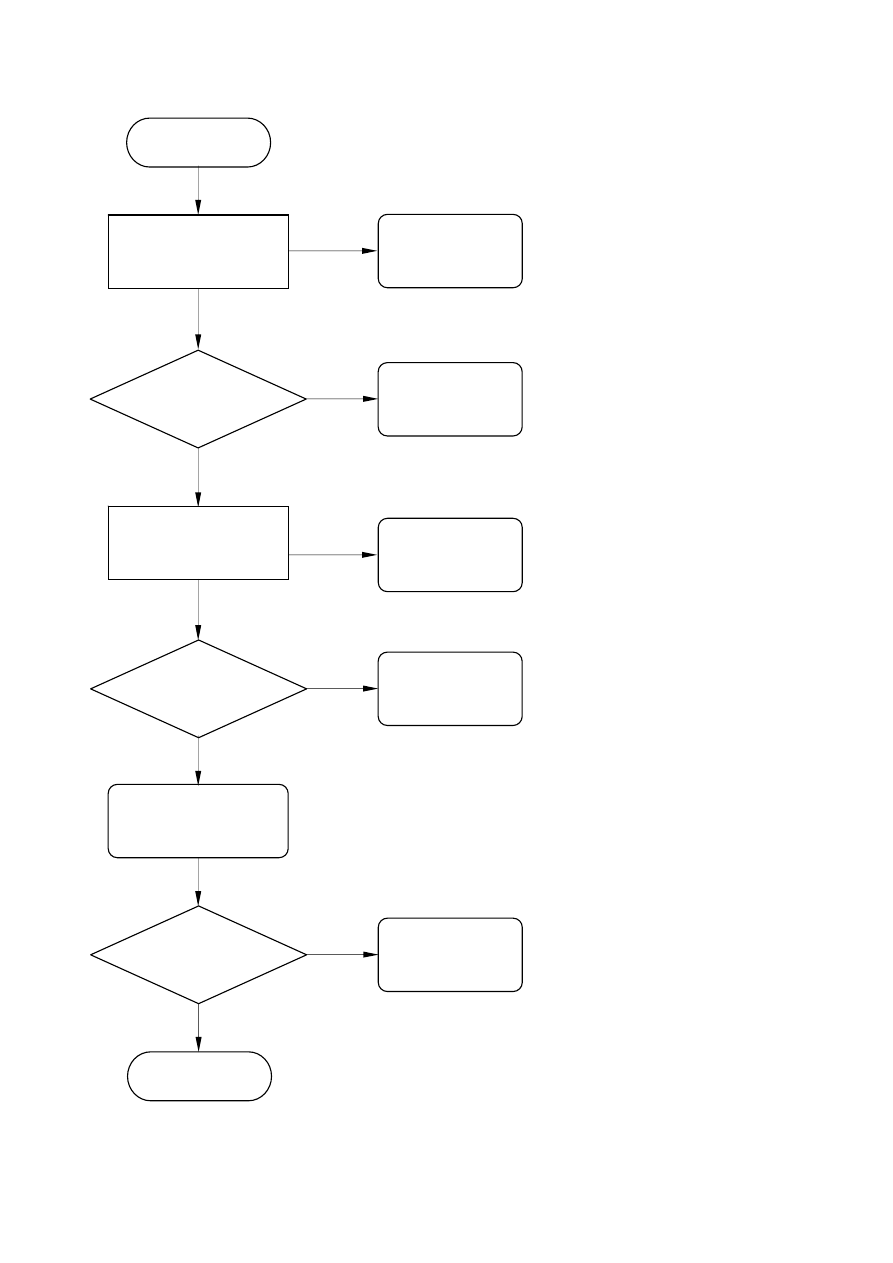
I. TROUBLE SHOOTING HINTS
NO NO
YES YES
YES
YES
NO
NO
High Voltage !
NO
YES
YES
NO
NO
YES
No
Display
( Bl
k )
LED ON
?
Push the power
ON/OFF
switch
LED Color
change ?
Check main
board
U10/Pin141
Hi / Lo under
push power
sw?
Back light
ON?
To Step 2
Make sure the
connection of
Inverter is fine
+12V ?
Check the
CN1
/Pin1
of Inverter
Check
F1(Fuse) of
inverter
B
Display ?
OK !
A
To Step 2
Power
adapter ?
Change
adapter
15
NO
YES
YES
NO
YES
NO
B
Hi / Lo under
push power
sw?
Change the
Inverter
Display ?
OK !
To Step 2
A
Check the
connection
of
CN8
cable
Display ?
OK !
Change the
main board
Change the
main board
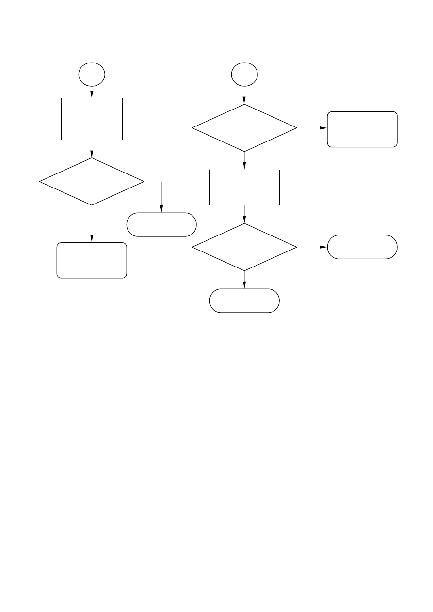
16
NO
YES
NO
YES
YES
YES
YES
NO
NO
YES
Step 2
Check the main
board
12V
?
+5.0 V ?
Check
U13,U14,R65
H/V input
Signal ?
Check the main
board
U10
/
Pin 146
?
Change
U11
Check
H/V Signal
Display ?
OK !
Change
Signal Cable
Check
F1,D5
Check
U10
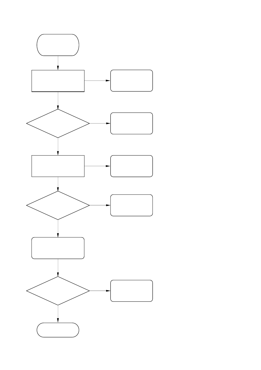
17
NO
YES
NO
YES
NO
YES
YES
NO
NO
YES
No display
(White)
Check the main
board
5V
?
+3.3V ?
H/V Input
Signal ?
Check the main
board
U11/Pin14
?
Change
U11
Check
H/V Signal
Display ?
OK !
Change
Signal Cable
Check
U13,U14
Check
U1,U13
Check
3.3V Circuit

18
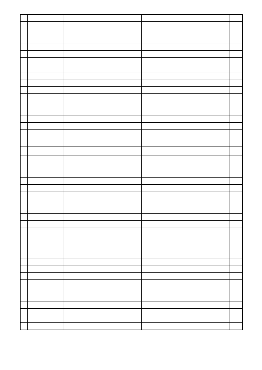
J. REPLACEMENT PARTS LIST
NO
Parts No.
Description
Part Location
Q’ty
988-AZ0-1006 HD972
1 002-001-TCO9
TCO99 Declaration
1
2 003-401-0565
Carton Label 90x70mm
MAG
1
3 003-A51-HD772
I/O Label
1
4 003-H01-AS576
TCO99 Label
For Front Bezel
1
5 005-503-HD972
Carton
For PROVIEW Logo
1
7 153-005-0765
Back Label
No Brand
1
8 160-02L-HD772
END Cap L EPS
1
9 160-02R-HD772
END Cap R EPS
1
10 170-000-0848C
PE Bag 0.07mm 14*30.5cm
1
11 170-001-LCD5
LCD PE Bag
550 x 800 x 0.06mm
1
12 170-005-VM541
PE Bag 300 x 200mm
For User Manual
1
13 170-500-AS776
Base Bag 360x360mm 0.03t
For Attachment
1
14 600-151-1000A
Power cord
1.5m Black VDE
15 621-151-2500C
Audio Cable
1
16 846-120-E0AL-SA Adapter LSE 60W
1
17 002-U51-HD772-A User Manual
1
999-XFA-HD972
899-002-HD972-E HD972 Main Board Ass’y
1 506-524-LC21
Memory IC 24LC21 SMD
U2
1
2
506-CXX-MVPRL-HN
MRT Scaler IC MVPRL-HN
U4
1
3 481-LCC-0440
SOCKET 44PIN PLCC
PP1
1
4 506-5NM-24C16
24C16 SO8 Memory IC SMD
U6
1
5 506-RLD-1117-A
LD1117 SMD UTC
U7
1
6 506-0AI-CY33
AIC1117-33 3.3V 900ma SMD
U8
1
7 518-1CE-9435
MOSFET CE9435A S08
U9,U10
2
8 506-1LM-3485
LM3485 SOP-8
U11
1
9 506-ALM-4838
Audio Amp IC LM4838
U12
1
10 531-120-49US
Crystal 12 MHz 49US
Y1
1
11 531-110-49US
Crystal 11 MHz 49US
Y2
1
12 528-200-BAV99
Hi Speed Switch Diode BAV99
Q1,Q2,Q3
3
13 518-02N-3906
Tr. 2N3906 SMD
Q14
1
14 518-02N-3904
NPN 2N3904S SMD
Q15,Q16,Q17,Q18,Q19,Q20 6
15 529-350-05R1
Zener Diode MSZ5231B 5.1V
D1,D3,D4,D5
4
16 528-2BA-T54C
SMD Diode BAT54C SOT23
D2
1
17 528-R1N-4148
Diode 1N4148 SOT-34 SMD
D7
1
18 520-007-5822
Diode IN5822 30A/3A
TD1
1
19 745-330-2062-3
Choke 5A 33uH 20%
TL1
1
20 780-103-3000B
FBM-10-160808-300T/KTNG Core
L2,L6,L10
3
21 780-112-8000
SMD Bead 6A 80ohm 1812
L5,L29,L34
3
22 780-103-3000
SMD Bead SBK160808300Y0603 30Ω L13,L14,L15,L16,L20
5
19
23 780-104-8000A
SMD Bead
L17,L18,L19,L23,L24,L25,L30,L31,L33 9
24 281-035-3304
RES 33ohm 5% 1/10W 0603 SMD
L3,R5,L7,R9,L11,R14,R15,R72,R73 9
25 506-10E-8050
MCU MXIC MX10E8050I PLCC44
U5
1
26 558-352-5000
SMD Fuse 1206 24V 5A
F1
1
27 485-415-S060A
D-SUB Connector
CN1
1
28 630-008-C001
Header 1.5mm
CN4
1
29 630-006-C001
Base 6Pin Pitch=1.5mm
J1
1
30 409-003-0110
DC Jack 3.5D
CN10
1
31 630-002-1008
Base 2Pin Pitch=2.0mm
CN17,CN20
2
32 409-003-0111-H
RCA Jack 3.5D Red
CN19
1
33 409-003-0112-H
RCA Jack 3.5D White
CN18
1
34 281-031-68014
SMD R 6.8K 0603 1%
R83
1
35 281-031-20014
SMD R 2K 1% 0603
R84
1
36 282-103-2454
RES-NET 10Kohm 5% SMD 8P4R
RP1,RP2,RP3
3
37 281-031-75R04
SMD R 75 0603 1%
R1,R2,R3,R140,R141,R142 6
38 281-035-2224
RES 2.2K 5% 1/10W 0603 SMD
R7
1
39 281-035-1034
RES 10K 5% 1/10W 0603 SMD
R11,R12,R13,R25,R26,R28,R30,R33,R41,R49,
R55,R98,R100,R109,R114,R122,R131,R132
18
40 281-035-1024
RES 1K 5% 1/10W 0603 SMD R27,R29,R42,R47,R54,R56,R65 7
41 281-035-1014
RES 100ohm 5% 1/10W 0603 SMD
R6,R10,R31,R32,R66,R67,R68,R69,R70,R134,
R135,R143,R144
13
42 281-035-0R04
RES 0ohm 5% 1/10W 0603 SMD R35,R39,R40,R43,R120,R121,R130 7
43 281-035-1054
RES 1M 5% 1/10W 0603 SMD
R45,R95
2
44 281-035-3314
RES 330 5% 1/10W 0603 SMD
R48,R57
2
45 281-035-1044
RES 100K 5% 1/10W 0603 SMD
R81
1
46 281-035-1214
RES 120ohm +-5% 1/10W 0603 SMD
R77,R78
2
47 281-035-3334
RES 33K 5% 1/10W 0603 SMD
R76,R102,R113,R116
4
48 281-035-2034
RES 20K 5% 1/10W 0603 SMD
R101,R104,R105,R106,R107,R108,R111,R112 8
49 281-035-7534
SMD R 75K ohm 0603
R82
1
50 381-151-032554
SMD CC 150PF 25V NPO 0603 +-5%
CP1
1
51 382-153-035064
SMD CC 0.015uF/50V X7R 0603 +-10%
CZ1
1
52 385-104-035084
SMD Y5V 0.1uF 50V 0603
C2,C5,C8,C17,C29,C35,C36,C37,C44,C46,C50,
C53,C55,C56,C58,C60,C61,C62,C63,C67,C68,
C69,C70,C71,C72,C73,C76,C78,C80,C87,C90,
C91,C92,C93,C94,C95,C97,C96,C99,C102,
C104,C105,C114
43
53 381-220-035054
SMD CC 22pF 50V NPO 0603
C11,C12,C15,C16,C21,C22,C48,C49,C65,C66 10
54 382-103-032564
SMD CC 0.01uF/25V X7R 0603 +-10%
C34,C39,C40,C52,C54,C57,C77,C86 8
55 382-472-032564
Y5V 4700P/25V +80%-20% 0603
C38,C41,C42
3
56 381-331-032554
SMD CC NPO 25V 330PF 5% 0603
C101
1
57 330-470-16255
EC 47uF 16V 105C
TC1,TC6,TC9,TC11,C103
5
58 382-683-031664
SMD CC 0.068uF X7R 0603 +-10%
C106,C111
2
59 330-101-16255
EC.100uF/16V 5mm 105C TC2,TC3,TC4,TC5,TC8
5
60 330-100-16255
EC 10uF 16V H7mm
TC24
1
61 330-221-16255
EC. 220uF/16V 5mm 105C
TC7,TC10,TC12,TC13,TC14,TC15,TC16,TC21,
TC22,TC23
10
62 200-100-765S2-A M/B For 765S2 REV:A
1
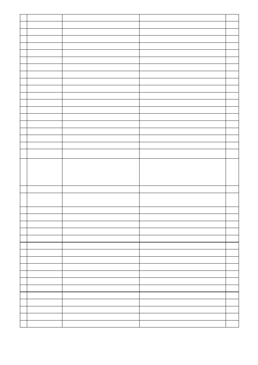
20
63 152-000-SH570
DC Jack support Nylon
1
64 385-334-031684
Chip-C 0.33u/16V 0603 Y5V
C107,C110
2
65 630-026-R2006
Base 2.0mm
JP1
1
66 529-350-05R6
SMD Zener 5.6V
D9
1
67 120-001-HD772
Heatsink 28x28x5.9mm
1
899-200-HD772
Power Board Ass’y
1 200-001-HD572-A Sensor Board
1
2 401-170-0200
Tact Switch
SW1
1
3 630-005-C001
Base 1.5mm 5Pin
J1
1
4 520-005-L317
LED 3D2P Green/Orange
D1
1
5 154-051-HD772
LED Holder
For D1
1
6 631-001-4004
Wire 4.3D Terminal UL1015 AWG18
Power Ground wire
1
899-400-HD772
Control Board Ass’y
1 200-701-0772
Control PCB
1
2 401-170-0200
Tact Switch
SW1,SW2,SW3,SW4,SW5,SW6 6
3 630-005-C001
Base Pitch=1.5mm 5Pin
J1
1
4 705-590-950A
19” AU Panel M190EN02
1
5 849-4AS-0772-A Inverter
1
902-HD0-A017
1 100-006-3062
Screw R3*6mm TP+ISO
Main PCB to Panel Bracket x 4,
Inverter to Panel Bracket x2, Shield Coverx2
8
2 100-010-3012
Screw R3x10mm TP1
Main PCB to Bezel x2, Panel Bracket to Bezel x8
Speaker(L) to Bezelx4, Speaker(R) to Bezelx4
Panel Bracket (L) to Bezelx7,
Panel Bracket (R) to Bezelx7,
Panel Bracket Bottom to Bracketx2,
Panel Bracket Bottom to Bezelx3,
28
3 107-008-4072
B 4*8mm TP4
Hinge to Housing
4
4 107-010-3073
B 3*10mm TP4
Housing to Bezel*6, Housing to Panel Bracket*2,
Panel Bracket (L) to Panel*2,
Panel Bracket (R) to Panel*2
12
5 108-S14-4032
Screw B/SW 4*14mm ISO
Hinge to Stand
1
6 109-948-0860
Screw
For D-Sub connector
2
7 121-001-HD772
Support Stand
1
8 121-750-HD772
Stand
1
9 121-002-HD772
Support Base
1
10 121-751-HD772
Base
1
11 121-500-HD972
Bracket R SECC 1.0t
1
12 121-501-HD972
Bracket L 1.0t
1
13 121-502-HD972-A Panel Bracket
1
14 121-52B-HD972
Bracket B
1
15 123-500-HD972
Bracket Shield Cover SPTE 0.3mm
1
16 126-001-HD772
Hinge
1
17 132-300-PS576
Base Screw Ass’y
1
18 106-012-6033
Screw M6 L 12mm
Fixed Base & Neck
1
19 132-001-PS576-A Springe
1
20 151-A01-I92S4
Front Bezel
Proview
1
21 154-002-HD772
Housing Cover
ABS 1
21
22 154-502-HD872
IR Lens
Pantone 195U
1
23 154-500-HD972
Power Knob
EM-00SL
1
24 154-501-HD972
Power Lens
1
25 154-502-HD972
OSD Knob
EM-00SL
1
26 154-503-HD972
OSD Knob Cover
EM-00CB
1
27 155-110-0003
Rubber 10 Ø *3
For Support Base
4
28 610-151-15GM-4 Signal Cable
1
29 631-006-7014-T
Wire 100mm 2.0 24AWG
For Inverter
1
30 631-008-G0509
J1
1
31 824-002-772VL-A Speaker 8Ω 2W
Left side
1
32 824-002-772VR-A Speaker 8Ω 2W
Right side
1
33 831-B13-0303
L20*W13*H17mm
For Panel and Main Cover upper side
1
34 126-500-2004
AL Foil L200*W40mm
For Panel
4
35 126-030-ALP4
AL Foil 200*30mm
Main Cover and Panel Inverter
2
36 126-001-7540
AL Foil 75*40mm
For Speaker
2
37 126-030-ALP
AL Foil 150*30mm
Bottom Bracket and Panel
1
38 126-A50-0972
AL Foil 320*50mm
Main Cover and Panel Inverter
1
39 631-001-4025A
Wire 1007#22 Black 250mm
Rear Cover to Main Cover Ground
1
40 101-008-3012
SCrew R3*8mm TP1
OSD Knob Cover to Bezel
2
41 104-008-3012
Screw R/W 3*8MM tp1
For Control PCB
2
42 154-509-HD772
Mylar Plate 85*58mm
1
43 123-501-HD972
Bracket shield Cover 0.3t
1
44 631-A30-S972
LVDS Wire 150mm
1
45 650-003-0081
Cable Tie
1
22
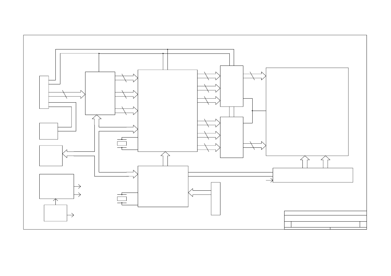
K. BLOCK DIAGRAM
ORION
B
BLOCK DIAGRAM
B
1
1
Tuesday, October 23, 2001
Title
Size
Document Number
Rev
Date:
Sheet
of
HSYNC
VSYNC
D-DE
BLK-ON/OFF
SDA
BRIGHTNESS
DDC-SCL
DDC-SDA
SCL
POWER
ADAPTER
12V
SWITCH POWER
SUPPLY AND
3V
5V
12V
C
O
N
N
E
N
T
VGA-IN
12PIN
D.D.C
24C21
EEPROM
ADC
SCALER
LVDS
LVDS
MCU
24C16
EEPROM
INVERTER
12V
C
O
N
N
E
N
T
FUNCTION KEY
8PIN
LCD PANEL(LVDS)
REGULATOR
CRYSTAL
CRYSTAL
3 {R.G.B}
12M HZ
12M HZ
8 R0~R7
8 G0~G7
8 B0~B7
8 RA0~RA7
8 GA0~GA7
8 BA0~BA7
8 RB0~RB7
8 GB0~GB7
8 BB0~BB7
10 ODD
10 EVEN
POWER
HI VOLTAGE
23
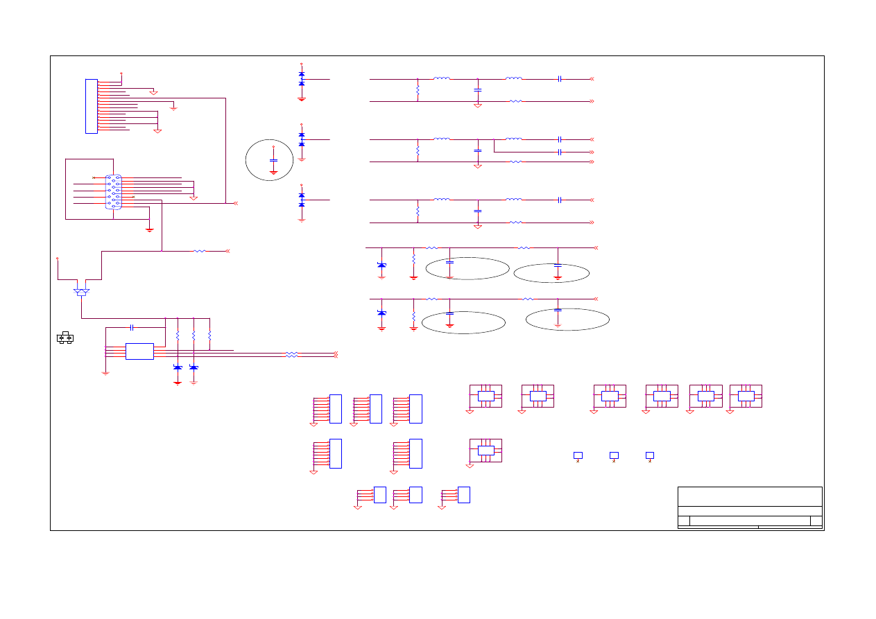
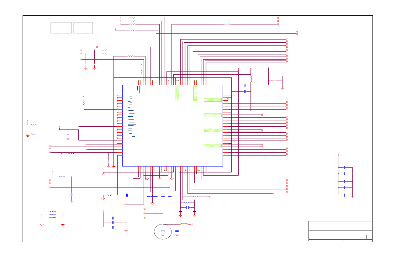
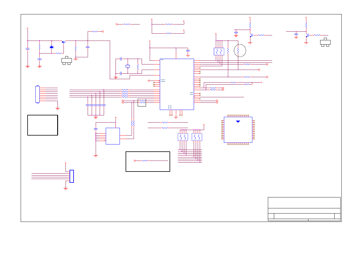
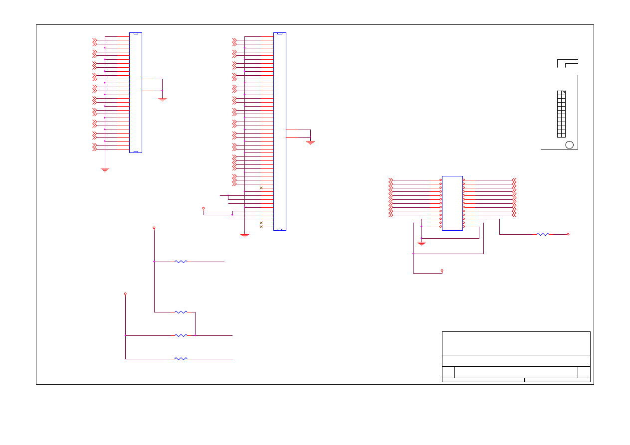
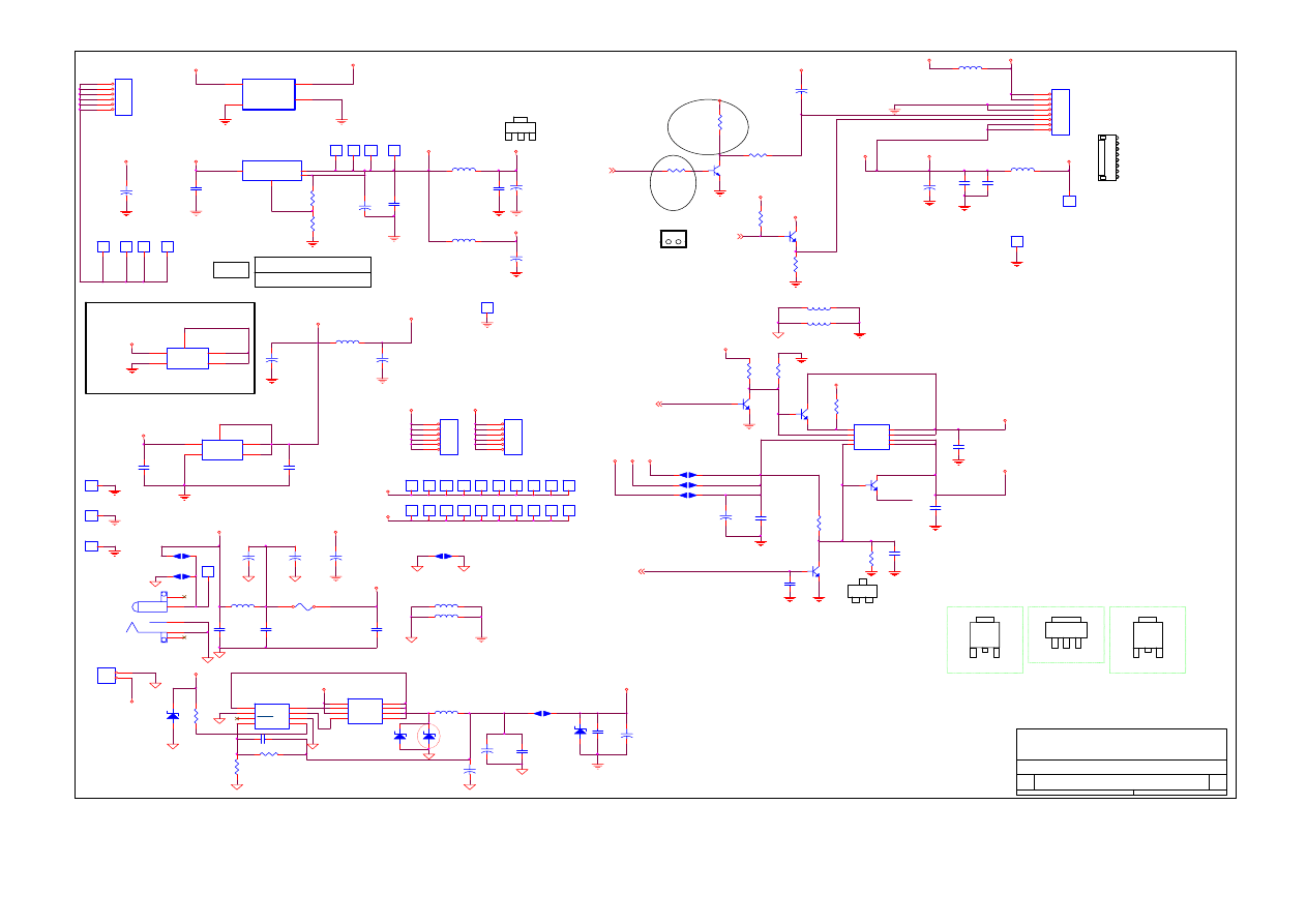
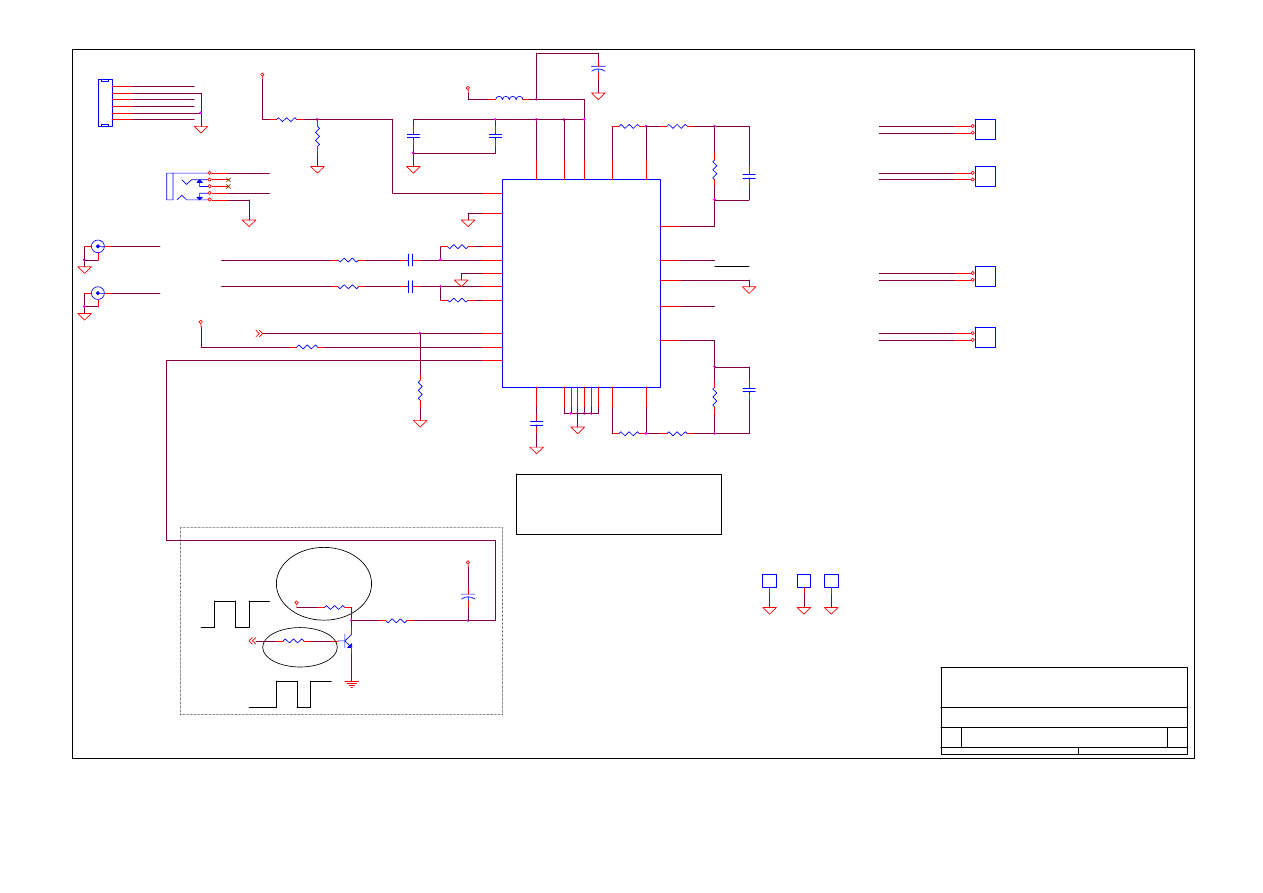
L. SCHEMATIC DIAGRAM
GND-RGB
C16
33pF
R142
75 1%
D3
ZD5.1
1
2
DDC-SCL
C9
NP
L2
30A
GND-RGB
H2
NP
1
1
R146
33
R7
2.2K
C11
33pF
R14
33
GND-DIG
IN-V
IN-V
BLUE
R5
33
L3
33
1
DDC-SDA
C5
0.1uF
BAT54C
IN-V
H3
NP
1
1
H18
NP
1
2
3
4
5
6
7
8
R140
75 1%
L6
30A
RE D-
2
IN-H
GND-PWR
C12
33pF
G RE E N-
2
BLUE+
2
Q2
BAV99
1
3
2
DDC-SCL
M1
NP
1
2
3
4
5
6
7
8
9
1
2
34
56
7
8
9
C6
NP
GND-RGB
C15
33pF
R11
10K
D5
ZD5.1
1
2
DDC-SCL
GREEN
M2
NP
1
2
3
4
5
6
7
8
9
1
2
34
56
7
8
9
GND-PWR-A
M5
NP
1
2
3
4
5
6
7
8
9
1
2
34
56
7
8
9
GND-DIG
INV DEL R
GND-DIG
C1
NP
H17
NP
1
2
3
4
5
6
7
8
CN1
V GA-DSUB15
1
6
2
7
3
8
4
9
5
11
12
13
14
15
10
16
17
GND-RGB
GND-RGB
H28
NP
1
2
3
4
L11
33
修改一
VCC
3
DDC-SDA
Q3
BAV99
1
3
2
R13
10K
GND_AUD
VCC
DC_12VIN
L10
30A
PC5V
CN15
JST2.0-1X16PIN
1
2
3
4
5
6
7
8
9
10
11
12
13
14
15
16
IN-H
BLUE
RED+
2
C4
0.1uF
R10
100
ISP_ON
3
H15
NP
1
2
3
4
5
6
7
8
L7
33
TxD
3
GREEN+
2
RED
Q1
BAV99
1
3
2
M4
NP
1
2
3
4
5
6
7
8
9
1
2
34
56
7
8
9
H11
NP
1
2
3
4
R1
75 1%
R18
NP
1
2
3
4
5
6
7
8
BLUE
HSY NC
2
RED
GND_AUD
U2
24LC02-SO8
1
2
3
4
5
6
7
8
NC
NC
NC
VSS
SDA
SCK
VCLK
VCC
GREEN
BLUE
DISPLAY
P1-VGA INPUT
1
6
Thursday , Nov ember 06, 2003
S3
Title
Size
Document Number
Rev
Date:
Sheet
of
M3
NP
1
2
3
4
5
6
7
8
9
1
2
34
56
7
8
9
GND-RGB
add
D2
B A T 54 C-S O T 23
1
3
2
VSY NC
2
R2
75 1%
R12
10K
C17
0.1uF
GND-DIG
SEFT_TEST
3
DDC-SDA
GND-DIG
IN-V
R96
NP
R6
100
R3
75 1%
M6
NP
1
2
3
4
5
6
7
8
9
1
2
34
56
7
8
9
RED
R9
33
M7
NP
1
2
3
4
5
6
7
8
9
1
2
34
56
7
8
9
IN-H
PC5V
R141
75 1%
D4
ZD5.1
1
2
B LUE -
2
S O G IN
2
R15
33
GND-DIG
GREEN
H10
NP
1
2
3
4
GND-DIG
VCC
H12
NP
1
2
3
4
5
6
7
8
RxD
3
GREEN
C8
0.1uF
C2
0.1uF
H1
NP
1
1
VCC
GND-PWR-A
RED
MRT Inc.
PROJECT : MVXPRL&MVPRL
D1
ZD5.1
1
2
2
VCC
C3
NP
24
FB0P_TX1+O
4
MVPRL
V AA3RGB
XXPIN33
EC100uF XX
BG2N
4
V DD
V DC2V
Y DIO
4
FCLKN
4
R28
10K
C46
0.1uF
TC2
100uF/16V
C50
0.1uF
C41
4.7nF
L13
BE121(0603)
TX3+O
4
TX2-
VREF
BXDIO
4
TX2+
FR2N
4
V DD
V DD
BR1P
4
FR0N_TX3-E
4
TX2-
R145
NP
C44
0.1uF
V AA2V
CFG[3:2]
RED+
1
Y OE
4
TC1
47u F/16V
BE0805
L19
FB1P_TX2+O
4
R29
1K
RE D-
1
Kaimin 0410
U4
MVPRL
1
2
3
4
5
6
7
8
9
10
11
12
13
14
15
17
18
19
20
21
22
23
24
25
26
27
28
29
30
31
32
33
34
35
36
37
38
39
40
41
42
43
44
45
46
47
48
49
50
51
52
53
54
55
56
57
58
59
60
61
62
63
64
65
66
67
68
69
70
71
72
73
74
75
76
77
78
79
80
120
119
118
117
116
115
114
113
112
111
110
109
108
107
106
105
104
103
102
101
100
99
98
97
96
95
94
93
92
91
90
89
88
87
86
85
84
83
82
81
160
159
158
157
156
155
154
153
152
151
150
149
148
147
146
145
144
143
142
141
140
139
138
137
136
135
134
133
132
131
130
129
128
127
126
125
124
123
122
121
16
AGNDP/CAP-V
AVDDP/Y 0
AVDDC/Y 1
RXCN/Y2
RXCP/Y 3
AGNDC/Y 4
AVDD0/Y5
RX0N/Y 6
RX0P/Y 7
AGND0/DIVDD3V
GND0/DIVSS
VDD0/DATA0
AVDD1/DATA1
RX1N/DATA2
RX1P/DATA3
GND1/DATA5
VDD1/DATA6
AVDD2/DATA7
RX2N/DCVDD2V
RX2P/DCVSS
AGND2/UV0
GND2/UV1
VDD2/UV2
DGND/UV3
DGND/UV4
DVDD/UV5
DCVDD2V/UV6
DCVSS/UV7
VDD3V
DGND
DTEST
VDD2V
VGA_VSY NC
VGA_HSY NC
VAA2V
GNDA
SOGIN
VAA3V
AGND
VR
E
F
CP
CZ
VA
A3
B
BI
N
+
BI
N
-
A
G
NDB
BC
LP
VT
OP
VB
OT
VA
A3
G
GI
N
+
GI
N
-
A
G
NDG
GC
LP
TO
UT
P
TO
UT
M
VA
A3
R
RI
N+
RI
N-
A
G
NDR
RCL
P
AD
V
D
D
3
V
AD
V
S
S
XT
AL
XT
AL
I
D
O
BV
SS
GPI
O
1
GPI
O
0
PW
M
1
ST
H
1
ST
H
8
LP
DO
B
V
D
D
3V
SH
C
RL
S
POL
V
DDC2
V
DCV
S
S
RG
ND
RVDD3V
RGND
RSBB3P
RSBB3N
RSBB2P
RSBB2N
RSBB1P
RSBB1N
RSBB0P
RSBB0N
TXPLLVDD3V
TXPLLGND
TxOUT0B-/RSAR3P
TxOUT0B+/RSAR3N
TxOUT1B-/RSAR2P
TxOUT1B+/RSAR2N
TxOUT2B-/RSAR1P
TxOUT2B+/RSAR1N
TxCLKB-/RSAR0P
TxCLKB+/RSAR0N
RSACKP
RSACKN
TxOUT3B-/RSAG3P
TxOUT3B+/RSAG3N
TxOUT0A-/RSAG2P
TxOUT0A+/RSAG2N
TxOUT1A-/RSAG1P
TxOUT1A+/RSAG1N
TxOUT2A-/RSAG0P
TxOUT2A+/RSAG0N
RVDD3V
RGND
TxCLKA-/RSAB3P
TxCLKA+/RSAB3N
TxOUT3A-/RSAB2P
TxOUT3A+/RSAB2N
RSAB1P
RSAB1N
RSAB0P
RSAB0N
CL
K
O
U
T
/C
A
P
-H
D
IVS
S/
C
A
P-
H
R
E
F
D
IV
DD3
V
/TV
CL
K
IR
Q
#
SC
S#/
H
F
S
#
SD
A
SC
L
RS
T
ST
V3
ST
V1
CP
V
OE3
/<C
ON
F
IG3
>
OE2
/<C
ON
F
IG2
>
OE1
/<C
ON
F
IG1
>
DCV
S
S
P
W
M
0/
<CO
NF
IG
0>
D
C
V
DD2
V
LCD_
V
E
E
LCD_
V
D
D
LCD_
V
B
L
DO
B
V
DD3
V
DO
B
V
S
S
RS
B
R
3P
RS
B
R
3N
RS
B
R
2P
RS
B
R
2N
RS
B
R
1P
RS
B
R
1N
RS
B
R
0P
RS
B
R
0N
RS
B
C
K
P
RS
B
C
K
N
RS
B
G
3P
RS
B
G
3N
RS
B
G
2P
RS
B
G
2N
RS
B
G
1P
RS
B
G
1N
RS
B
G
0P
RS
B
G
0N
AGND1/DATA4
C22
22pF
BCLKP
4
FG1P_TX1+E
4
TA
FXDIO
4
RESET_MASCOT
3
BR0P
4
B LUE -
1
CONFIG0
G ND-RGB
C40
0.01uF
C54
0.01uF
R42
1K
V DD
R25
10K
FR1N
4
BG0P
4
THIS IS FOR PIN 30
FR0P_TX3+E
4
R27
1K
VDC2V
BE0805
L17
C58
0.1uF
FB0N_TX1-O
4
TC5
47 uF/16 V
R39
0
Y1
12MHZ
R45
1M
C37
0.1u F
PIN 26 ADD R200&R201
R44
NP
BG1N
4
TXCK+E
4
BG2P
4
C42
4.7nF
C21
22pF
TXCK-E
4
CONFIG3
HSY NC
1
PWM1
6
G ND-DIG
R26
10K
G REE N-
1
BB0P
4
FG0P_TX0+E
4
S OG IN
1
R35
0
BB2N
4
CP1
150pF
C56
0.1uF
BR2N
4
V DD
BR1N
4
FB2P_TXCK+O 4
R30
10K
BE0805
L18
V DD2V
L16
BE121(0603)
IRQ -
3
BR2P
4
V DC2V
V DD
BG0N
4
BB1N
4
BB1P
4
FB1N_TX2-O
4
TX2+
TX3-O
4
VDDCTRL-1
5
POL
4
S DA
3
FG2P_TX2+E
4
FR1P
4
CONFIG2
VDDCTRL
5
XSTB
4
L20
BE121(0603)
FG0N_TX0-E
4
FB2N_TXCK-O 4
C52
0.01uF
BCLKN
4
FG2N_TX2-E
4
DISPLAY
P2-MVPRL
2
6
Thursday , Nov ember 06, 2003
S3
Title
Size
Document Number
Rev
Date:
Sheet
of
V DC2V
C49
22pF
MVPRL
R41
10K
BG1P
4
BR0N
4
V DC2V
TX0+O
4
C35
0.1uF
FG1N_TX1-E
4
C53
0.1uF
TX0-O
4
12M
3
C48
22pF
R40
0
C39
0.01uF
SCL
3
卡件改為100uF--->47uF
MVPRL
V DD
R31
100
R33
10K
BB2P
4
FCLKP
4
MRT Inc.
PROJECT : MVXPRL&MVPRL
V AA3RGB
PWM0
5
CFG[1:0]
0 0 -> I2C
0 1 -> SPI
1 0 ->
6-WIRE
V AA3RGB
FR2P
4
C55
0.1uF
C57
0.01uF
C38
4.7nF
VDD
C29
0.1uF
B LUE+
1
BB0N
4
V SY NC
1
C36
0.1uF
G REE N+
1
R32
100
Y CLK
4
VBLCRL
5
R43
0
CONFIG1
CZ1
15nF
25
R65
1K
5.UP
add
LED_GREEN
R130
0
R137
100
R55
10K
R49
10K
+
TC24
10uF/16V
RESET_MASCOT 2
6.MENU
R129
NP
L ED_ O
C61
0.1uF
P1-6
B
POWER
STBY & MUTE
ACTIVE HIGH
POWER
8.GND
R48
330
R54
1K
SCL
2
R136
100
UP
add
V CC_M CU
V CC_M CU
V CC_M CU
2
P1-2
P1-0
PROVIEW KEY PAD --OK
V CC_M CU
C65
22pF
RESET
B
P1-1
DOWN
TxD
2.0 mm
MENU
SDA
2
0814
VCC
R98
10K
U5
SOCKET_44PLCC
35
21
20
10
14
15
16
17
2
3
4
5
6
7
8
9
43
42
41
40
39
38
37
36
24
25
26
27
28
29
30
31
19
18
32
33
13
11
44
22
23
34
1
12
EA/VP
X1
X2
RESET
INT0 / P3.2
INT1 / P3.3
T0 / P3.4
T1 / P3.5
P1.0 / T2
P1.1 / T2EX
P1.2
P1.3
P1.4
P1.5
P1.6
P1.7
AD0 / P0.0
AD1 / P0.1
AD2 / P0.2
AD3 / P0.3
AD4 / P0.4
AD5 / P0.5
AD6 / P0.6
AD7 / P0.7
A8 / P2.0
A9 / P2.1
A10 / P2.2
A11 / P2.3
A12 / P2.4
A13 / P2.5
A14 / P2.6
A15 / P2.7
P3.7/ RD
P3.6 / WR
PSEN
ALE
P3.1 / TXD
P3.0 / RXD
VC
C
VS
S
P4
.0
P4
.1
IN
T
3 / P
4.2
IN
T
2 / P
4.3
VCC
P1-4
3.LED G
RESET_MASCOT 2
C63
0.1uF
LED_GREEN
12MOUT
1
TxD
1
P1-1
1
RxD
C
IRQ-
2
C7
0
0.
1uF
C73
0.1uF
SDA
2
TxD
E
0818
P1-0
RxD
P1-6
LED_G
PSEN
RP1
10KX4
1
2
3
4
8
7
6
5
R95
1M
P1-3
R70
100
12MOUT
修改二
SCL
Q16
2N3904
3
1
2
LED_G
R138
NP
2.LED O
0818
RxD
Q15
2N3904
3
1
2
R131
NC
R143
NP
R72
33
R132
NC
R144
NP
SCL
2
ISP_ON
1
LED_ORANG
P1-6
V CC
P1-4
RP2
10KX4
1
2
3
4
8
7
6
5
V CC_M CU
AUTO
AUD_OFF
6
LED_O
U6
24LC16B-SO8
1
2
3
4
5
6
7
8
A0
A1
A2
VSS
SDA
SCL
WP
VC
C
2
V CC_M CU
PSEN
R66
100
V CC_M CU
C7
1
0.
1uF
DISPLAY
P3-MCU
3
6
Thursday , Nov ember 06, 2003
S3
Title
Size
Document Number
Rev
Date:
Sheet
of
RESET
R147
10K
C60
0.1uF
RxD
1
LED_ORANG
C6
8
0.
1uF
MENU
UP
P1-3
0818
P1-7
R68
100
R64
NP
R134
NP
R135
NP
7.AUTO
3
Y 2
11.0592MHZ
CN4
JST-S8B-ZR
1
2
3
4
5
6
7
8
1
2
3
4
5
6
7
8
TxD
SDA
VGA 11 ISP_TX
VCC
R46
NP
CN5
JST1X8(NP)
1
2
3
4
5
6
R47
1K
R57
330
C67
0.1uF
R69
100
D7
1N4148
1
2
C7
2
0.
1uF
DOWN
1.Power
C
VDD
AUTO
P1-7
C66
22pF
P1-7
R56
1K
4.DOWN-
VGA 4 ISP_TX
R50
4.7K
PP1
MXIC 3552
1
2
3
4
5
6
7
8
9
10
11
12
13
14
15
16
17
18
19
20
21
22
23
24
25
26
27
28
29
30
31
32
33
34
35
36
37
38
39
40
41
42
43
44
SEFT_TEST
1
P1-5
E
R67
100
R73
33
C6
9
0.
1uF
P1-5
C62
0.1uF
12M
2
RP3
10KX4
1
2
3
4
8
7
6
5
P1-2
Q14
2N3906
3
1
2
3
26
FR2P
2
BCLKN
2
FB0N_TX1-O
2
VDD_JP
BR1P
2
FG1P_TX1+E
2
BB0N
2
FB1P_TX2+O
2
LCDVDD
FB0P_TX1+O
2
FG0N_TX0-E
2
R133
NP
24
CPT 17 PIN42& PIN43 3.3V &
PIN44 & PIN46 & PIN47 &
PIN48 12V
AU 17 & QDI 17 R120-->0
1
FOR 17" FB501,FB503,
R505,R506,R507,R508,R510,
Q502,C504 NC
FB2P_TXCK+O
2
QDI 17 R117-->0
XSTB
2
FB1N_TX2-O
2
FR0P_TX3+E
2
FG2N_TX2-E
2
LCDVCC
VDD
TX0-O
2
BB1P
2
AU17 42 43 NC. 44 46 47 48 = 5V.
HS15 42 43 44 = 3.3V 46 47 =12V
48 49 50 NC.
BR2P
2
FG0N_TX0-E
2
BB0P
2
FR1P
2
R119
NP
CPT 17 R117-->0
FG1N_TX1-E
2
LCDVCC
YDIO
2
BXDIO
2
BR2N
2
FG2N_TX2-E
2
FB0N_TX1-O
2
23
AU 17 & QDI 17 R121-->0
POL
2
FB2N_TXCK-O 2
FG1P_TX1+E
2
FOR 15"
FB502,FB504,FB505
R504,R510, NC
FG2P_TX2+E
2
FR0N_TX3-E
2
R120
0
2
BB2N
2
YCLK
2
FR1N
2
AU 17 & QDI 17 R120-->0
FCLKP
2
CPT 17 3.3V
PIN42O
1
FB1N_TX2-O
2
TX3-O
2
BG0P
2
FCLKN
2
PIN48O
LCDVCC
BG0N
2
CPT 17 12V
BG2P
2
FXDIO
2
QDI 15 PIN42& PIN43& PIN44
3.3V R117-0 R119-0 R120-0
R121-NP
FR0N_TX3-E
2
FB0P_TX1+O
2
BR0P
2
BCLKP
2
TX3+O
2
PIN44O
FG2P_TX2+E
2
2
TX0+O
2
MRT Inc.
PROJECT : MVXPRL&MVPRL
DISPLAY
P4-OUTPUT
4
6
Thursday , Nov ember 06, 2003
S3
Title
Size
Document Number
Rev
Date:
Sheet
of
BB1N
2
FG1N_TX1-E
2
BB2P
2
FB2P_TXCK+O
2
TXCK-E
2
FB1P_TX2+O
2
FB2N_TXCK-O
2
BR1N
2
TXCK+E
2
PIN48O
BG2N
2
BR0N
2
R117
0
PIN44O
AU 17 & QDI 17 R120-->0
R121
0
BG1P
2
BG1N
2
CN6A
FH12-30S-0.5SH
30
29
28
27
26
25
24
23
22
21
20
19
18
17
16
15
14
13
12
11
10
09
08
07
06
05
04
03
02
01
30
29
28
27
26
25
24
23
22
21
20
19
18
17
16
15
14
13
12
11
10
09
08
07
06
05
04
03
02
01
32
31
FR0P_TX3+E
2
YOE
2
CN7A
FH12-50S-0.5SH
50
49
48
47
46
45
44
43
42
41
40
39
38
37
36
35
34
33
32
31
30
29
28
27
26
25
24
23
22
21
20
19
18
17
16
15
14
13
12
11
10
09
08
07
06
05
04
03
02
01
50
49
48
47
46
45
44
43
42
41
40
39
38
37
36
35
34
33
32
31
30
29
28
27
26
25
24
23
22
21
20
19
18
17
16
15
14
13
12
11
10
09
08
07
06
05
04
03
02
01
52
51
JP1
HEADER 12X2
1
2
3
4
5
6
7
8
9
10
11
12
13
14
15
16
17
18
19
20
21
22
23
24
26
25
0814
LCDVCC
FG0P_TX0+E
2
PIN42O
FR2N
2
AU 17 R117-->NP
FG0P_TX0+E
2
27
GND-PWR-A
TC4
10 0u F/1 6V
MRT Inc.
PROJECT : MVXPRL&MVPRL
1
ADJ/GND
12V
0818
AU S6 SHORT
GND-DIG
C77
0.01uF
Brightness
GND-DIG
LT1117-ADJ R130-120
毆姆
R83
6.2K_1%
H14
TP
1
1
R77
120
J22
1
1
S2
2
1
Q19
2N3904
3
1
2
VCC
VDDCTRL-1
2
S9
2
1
3
VBLCRL
2
L29
BE1812-POWER
DC_5VOUT
INVERTER_ON
2
OUT
3-4
R76
4.7K
H21
TP
1
1
CN10
DC-JACK180
5
4
3
2
1
90@
1
ADJ/GND
I
VDD
J40
1
1
LT1117CST-2.5
SOT-252
4 Vout
B
C80
0.1uF
H22
NC
1
1
12V
J33
1
1
L14
BE121(0603)
F1
FUS1206-5A
H5
NP
1
1
+
TC16
470uF/16V
APL1117
DC_12VIN
C93
0.1uF
H25
NC
1
2
3
4
5
6
J31
1
1
VCC
+
TC13
470uF/16V
12V
2
OUT
L24
BE 0 80 5
6
J28
1
1
+
TC14
470uF/16V
J21
1
1
-25CE
AU 17 R16
不接
12V
VCC
TD1
1N5822
2
1
0814
VCC
PWM0
Q23
SI2301(OPT)
3
1
2
TC6
47uF/16V
1
2
TESTPOINT 5V
LCDVCC
12V_INV
V DC2V
V DC2V
PWM0
2
R75
4.7K
APL1117
LT1117-2.5V R131-0
甌姆
LT1117-ADJ R13-120
毆姆
VDD_A
H13
NC
1
1
DC_12VIN
BE0805
L30
V DD
J43
1
1
O
12V
R79
4.7K
C92
0.1uF
1
2
VCC
L25
BE 0 80 5
R16
0
SOT-223
H9
1
1
-33CE
V DD
GND-PWR-A
G
2
VCC
GND-DIG
U11
LM3485
1
2
3
4
8
7
6
5
VIN
DUTY
SHDN
FB
CS+
CS-
DRI
GND
H19
TP
1
1
R124
100K
VDD_A
+
TC12
470uF/16V
J26
1
1
J39
1
1
BK_ADJ
U9
Si9933-SO8
1
2
3
4
8
7
6
5
S1
G1
S2
G2
D1
D1
D2
D2
C
GND-DIG
VCC
R78
120
S5 NP
2
1
1
+
TC9
47uF/16V
R82
75K
1
ADJ/GND
V AA2V
TC3
10 0u F/1 6V
U7
LT1117-ADJ
1
2
3
4
AD
J
VOUT
VIN
TAB
VCC
V DD2V
C99
0.1uF
O
12V
J24
1
1
UA7
AIC1739(OPT)
3
1
2
4
VIN
VOUT
GND
VO1
R80
4.7K
J36
1
1
Q18
2N3904
3
2
1
TL1
47UH@5ADIP
H23
1
1
R122
10K
L15
BE121(0603)
VCC
U8
1117-3.3
1
2
3
4
5
ADJ
VO1
VIN
VO2
VO3
3
IN
12V_INV
C97
0.1uF
R81
100K
C91
0.1uF
R123
4.7K
2
LCDVDD
5-6
J37
1
1
VDDCTRL
2
J41
1
1
LT1117-2.5V R130-NP
V DD
BK_ADJ
BE0805
L31
U10
Si9435-SO8
1
2
3
4
8
7
6
5
S1
S2
S3
G
D4
D3
D2
D1
L23
B E 08 05
J29
1
1
D9
ZD5.6V
1
2
C34
0 .01 uF
C95
0.1uF
S8
2
1
4
E
VCC
VDD_A
GND-DIG
+
TC10
470uF/16V
S7 SHORT
2
1
Q22
SI2301(OPT)
3
1
2
J27
1
1
4 Vout
VCC
3
IN
V DD
+
TC15
470uF/16V
VCC
5V
DISPLAY
P5-DCPOWER
5
6
Thursday , Nov ember 06, 2003
S3
Title
Size
Document Number
Rev
Date:
Sheet
of
GND-PWR-A
L34
BE1812-POWER
修改2
J42
1
1
C78
0.1uF
C102
0.1uF
R84
2K_1%
J35
1
1
4 Vout
CPT S7 SHORT
H7
1
1
H4
NC
1
1
C87
0.1uF
DEFAULT
= 0
J38
1
1
CNA10
BASE2S
1
2
J34
1
1
SOT-223
V DD
C94
0.1uF
H20
TP
1
1
C101
330pF
2.00mm
VCC_INV
H8
NC
1
2
3
4
5
6
1
V AA3RGB
12V
APL1085
0814
CN8
JST-2.0-6PIN
1
2
3
4
5
6
7
8
+
TC21
470uF/16V
R74
1K
D10
NP
2
1
SOT-252
J25
1
1
L5
BE1812-POWER
1-2
D11
NP
1
2
Q17
2N3904
1
3
2
3V
C76
0.1uF
VDD
H6
1
1
2
OUT
+
TC23
470uF/16V
C90
0.1uF
H24
NC
1
2
3
4
5
6
S1
2
1
INVERTER_ON
Q21
NP
3
1
2
0814
GND_AUD
3
C96
0.1uF
TC7
470uF/16V
GND-DIG
V DD
GND-PWR-A
U13
1084-3.3(OPT)
1
2
3
4
5
ADJ
VO1
VIN
VO2
VO3
C86
0.01uF
S6 NP
2
1
+
TC22
470uF/16V
+
TC8
100uF/16V
J30
1
1
3
IN
J23
1
1
VDD_A
J32
1
1
1
28
VCC
TC11
47uF/16V
1
2
Right_Outp
Lef t_outp
RIGHTIN
R112
20K
0
HI SHUTDOWN
C111
0.068uF
Lef t_Outm
CN20
BASE2S
1
2
1
GAIN
R109
10K
RIGHTIN
Lef t_Outm
LEFTIN
Right_outm
R114
1K
R115
4.7K
MODE VCC OP VOL
R101
20K
AUD4835_DCVOL
R
VCC
Right_outm
R113
33K
R106
20K
0
C110 0.33uF
PWM1
2
AUD4835_SD
U12
NS4838&APA4835A
1
8
14
20
23
6
16
27
2
3
4
5
7
9
10
11
12
13
28
26
25
24
22
21
19
18
17
15
29
GN
D
GN
D
GN
D
GN
D
GN
D
VD
D
VD
D
VD
D
Shutdown
Gain Select
Mode
Mute
DC_Vol
Right Dock
Right In
Beep In
Lif t In
Lef t Dock
Right Out+
Right Out-
R
ight
Gai
n2
R
ight
Gai
n1
By
p
as
s
HP Sense
Li
ft
G
ai
n1
Li
ft
G
ai
n2
Lif t out -
Lif t out +
GN
D
LOW SP OUT
R102
33K
LEFTIN
VCC
C114
0.1uF
MUTE
Lef t_outp
CN16
BASE6
1
2
3
4
5
6
1
2
3
4
5
6
RIGHTIN
R107 20K
R
PA1
SCJ-0356M5(B)
1
2
3
4
5
L33
BE0805
1
2
R104
20K
HI HP OUT
R111
20K
HPS
L
AUD4835_DCVOL
H26
NC
1
1
Q20
2N3904
3
1
2
VCC
L
VCC_AU
RIGHTIN
LEFTIN
C104
0.1uF
R
CN3
BASE2-180°
1
2
R116
4.7K
CN17
BASE2S
1
2
CN2
BASE2-180°
1
2
Mute Hi is Mute
MODE
R108
20K
Gain Hi is Gain on
C105
0.1uF
MODE GND OP MAX
R105
20K
LEFTIN
Lef t_outp
R100
10K
SDWN
DISPLAY
P6-AUDIO
6
6
Thursday , Nov ember 06, 2003
S3
Title
Size
Document Number
Rev
Date:
Sheet
of
L
AUD_OFF
3
H27
NC
1
1
R110
NP
LEFTIN
Right_outm
C106
0.068uF
RIGHTIN
Right_Outp
CN19
SCP606
C107 0.33uF
CN18
SCP606
VCC
R103
NP
Shoutdown Hi is Shoutdown
0
H16
NC
1
1
Lef t_Outm
MRT Inc.
PROJECT : MVXPRL&MVPRL
Right_Outp
C103
47uF/16V
1
2
1

29
Memo
Wyszukiwarka
Podobne podstrony:
Proview RA783 LCD Service Manual
Proview PZ456 LCD Service Manual
Proview SH770I LCD Service Manual
Proview RA583 LCD Service Manual (Xerox)
Proview SH970I LCD Service Manual
Proview SH770 LCD Service Manual
Proview AY965 LCD Service Manual
Proview RA783 LCD Service Manual
Proview PZ456 LCD Service Manual
Proview SH770I LCD Service Manual
hplj 5p 6p service manual vhnlwmi5rxab6ao6bivsrdhllvztpnnomgxi2ma vhnlwmi5rxab6ao6bivsrdhllvztpnnomg
więcej podobnych podstron