Highly Integrated Information
Processing and Storage Systems
Professor L. Richard Carley
Center for Highly Integrated Information
Processing and Storage Systems
(www.chips.ece.cmu.edu)
Carnegie Institute of Technology
Carnegie Mellon University
&DUQHJLH 0HOORQ

L. R. Carley - “Highly Integrated Information Processing and Storage Systems” page 2 September 1999
&DUQHJLH 0HOORQ
CHIPS Team
• Center for Highly Integrated Information
Processing and Storage Systems (CHI
2
P
2
S)
• Current Research Team:
– L. Richard Carley, James A. Bain, Gary K. Fedder, Greg Ganger,
John Griffin, David W. Greve, David F. Guillou, Michael S. C. Lu,
Tamal Mukherjee, David Nagle, Suresh Santhanam, Steve Schlosser
Dept. of Electrical and Computer Engineering, Carnegie Mellon University
Leon Abelmann,
Information Storage Technology Group, MESA Research Institute,
University of Twente, Enschede, The Netherlands
Seungook Min
Dept. of Materials Science and Engineering, Carnegie Mellon University
• Support:
– DARPA ETO - Since 1993
– Industry: Intel, Texas Instruments, Infineon, Storage Tek
L. R. Carley - “Highly Integrated Information Processing and Storage Systems” page 3 September 1999
&DUQHJLH 0HOORQ
• Highly Integrated Info. Processing and Storage Systems
–
Processor (> 500 MIPS)
–
RAM (> 64 MB)
–
Nonvolatile Mass Memory (> 1 GB)
–
Communications (> 100 MB/s)
• IC Processing Based
–
Manufactured by IC
photolithographic techniques
(parallel manufacturing)
• Advantages of Integration
–
Less expensive
–
Smaller volume and mass
–
Lower power
–
Co-location of Storage and Processing
»
archival data storage / secure data
–
High shock resistance possible
–
NEW APPLICATIONS and NEW MARKETS
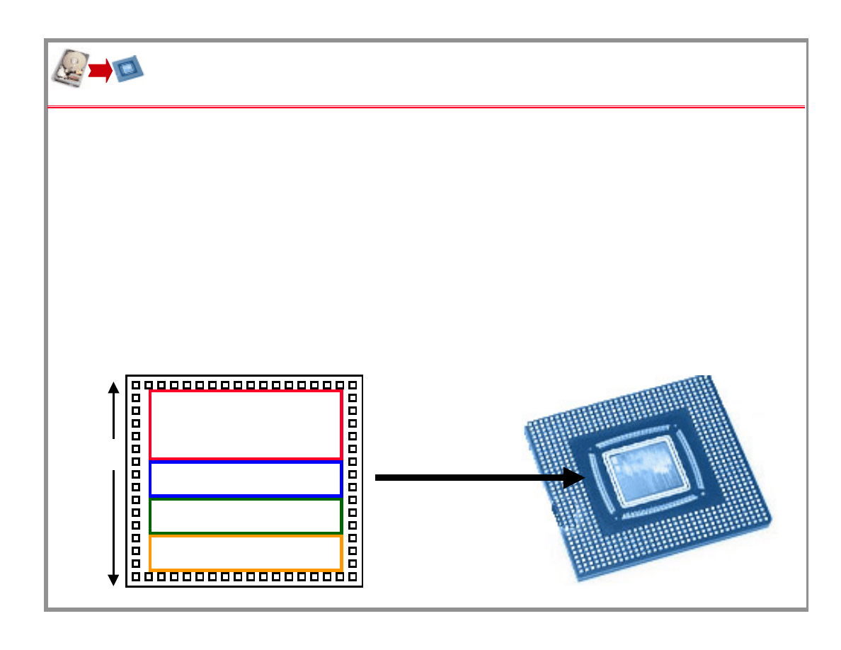
The Vision
2 cm
2 cm
CPU
RAM
Communications
Nonvolatile
Mass Memory

L. R. Carley - “Highly Integrated Information Processing and Storage Systems” page 4 September 1999
&DUQHJLH 0HOORQ
EEPROM for Mass Storage ??
• We have computers on a chip now - Embedded computers
– Billions of embedded CPUs sold today (vs. 100’s of millions of PC CPUs)
– How are HI
2
PS
2
systems different from “embedded computer” of today??
» Currently nonvolatile memory is EEPROM (FLASH memory)
» Dramatic increase in amount of nonvolatile mass memory (many GB)
» Quantum leap in kinds of applications possible; e.g., (1) a powerful OS!
(2) large data space, (3) complex programs, (4) learning (store history)
⇒
⇒
⇒
⇒
INTELLIGENT BEHAVIOR
• EEPROM Scaling vs. Time (
high voltage
⇒
⇒
⇒
⇒
hard to scale
):
– From Semiconductor Industries Association (SIA) Roadmap 1997/98
EEPROM 1997 1999 2002 2005
2008 2011
– NOR Cell Area 0.6µm
2
0.3µm
2
0.15µm
2
0.08µm
2
0.04µm
2
0.02µm
2
(density MB/cm
2
) 16 32 64 120
240 480
– EEPROM cost $/MB 6 3 1.5 0.8
0.4 0.2
(Best Case - no increase in fab cost / cm
2
)
– Expect IC-based mass storage at 10 GB/cm
2
by 2008
(>40X)
• Taking EEPROM prices as $0.4/MB
⇒
⇒
⇒
⇒
10 GB = $4,000 !!
– For IC-Based mass storage in 2008 predict < $40 / 10 GB
(> 100X better)
L. R. Carley - “Highly Integrated Information Processing and Storage Systems” page 5 September 1999
&DUQHJLH 0HOORQ
Motive: Lower Entry Cost
• Motivation:
– Possible new product niches
– Divisible cost
facilitates many applications
– Can be merged with DRAM & CPU(s)
• Goal:
– Complete computing & storage system
– $20 - $30
– 1 or a few IC substrates
• Example Applications:
– “throw-away” sensors / data logging systems
infrastructure monitoring; e.g., bridge monitors, concrete pours,
smart highways, condition-based maintenance, security systems,
low-cost speaker-independent continuous speech recognition, etc.
– “ubiquitous” use in everyday world
every appliance will be “smart” and “communicative”
– NOTE: embedded CPUs common, but no room for sophisticated code
» Intelligent behavior requires LOTS of SOFTWARE
0.01 GB
0.1 GB
1 GB
10 GB
100 GB
$1
$10
$100
$1000
CACHE RAM
DRAM
HARD
DISK
HI
2
PS
2
Entry Cost
Capacity @ Entry Cost (est. 2005)
L. R. Carley - “Highly Integrated Information Processing and Storage Systems” page 6 September 1999
&DUQHJLH 0HOORQ
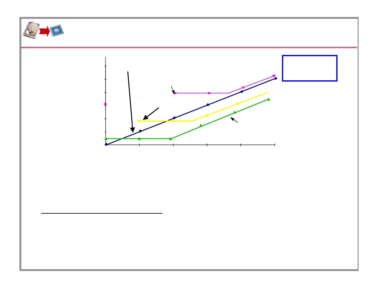
Motive: Low Volume & Mass
• 10 GB/cm
2
= 65 GB/in
2
density (100x CD-ROM)
• Expect stored bit size 20 nm x 20 nm bit size by 2009
• Example Applications:
» Space / satellite use - store data when not in line of site
act as packet buffer for communications satellites, etc.
» Human portable applications - e.g., medical implants, super PDA
» Law enforcement / monitoring devices / security surveillance
0.1
1
10
100
1000
10,000
0.1
10
100
1000
10,000
100,000
Storage Capacity [GB]
3.5” Disk Drive
Flash memory, 0.1 µm
2
/ cell (no packaging)
Occupied
volume [cm
3
]
HI
2
P
s
2
@ 10 GB/cm
2
(no packaging)
1
1” Disk Drive
Prediction
2005
L. R. Carley - “Highly Integrated Information Processing and Storage Systems” page 7 September 1999
&DUQHJLH 0HOORQ
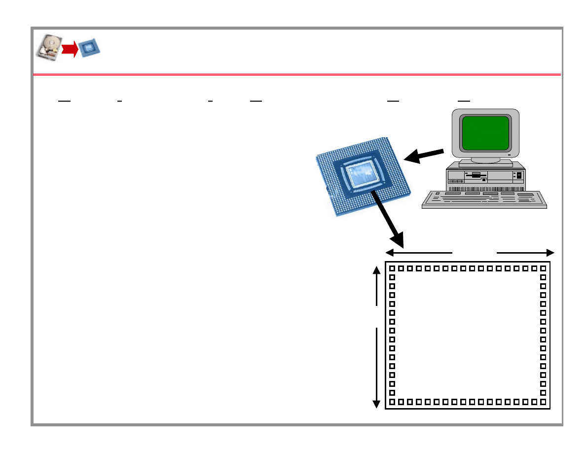
Motive: Storage System on a Chip
• Completely Integrated System
⇒
⇒
⇒
⇒
single chip = processing + mass storage
–
Enables new level of data archiving - push “lifetime” of data
»
Data reading hardware is archived with data
»
Software that can interpret data can be archived with data
»
Hardware that executes that software can be archived with data
»
Final interface can be simple long-lived standard one (e.g., RS-232)
–
Enables new level of “secure” devices
»
Internal IC lines extremely difficult to access
2 cm
USER DATA
Applic. Software
Hardware (CPU)
Generic Comm.
L. R. Carley - “Highly Integrated Information Processing and Storage Systems” page 8 September 1999
&DUQHJLH 0HOORQ
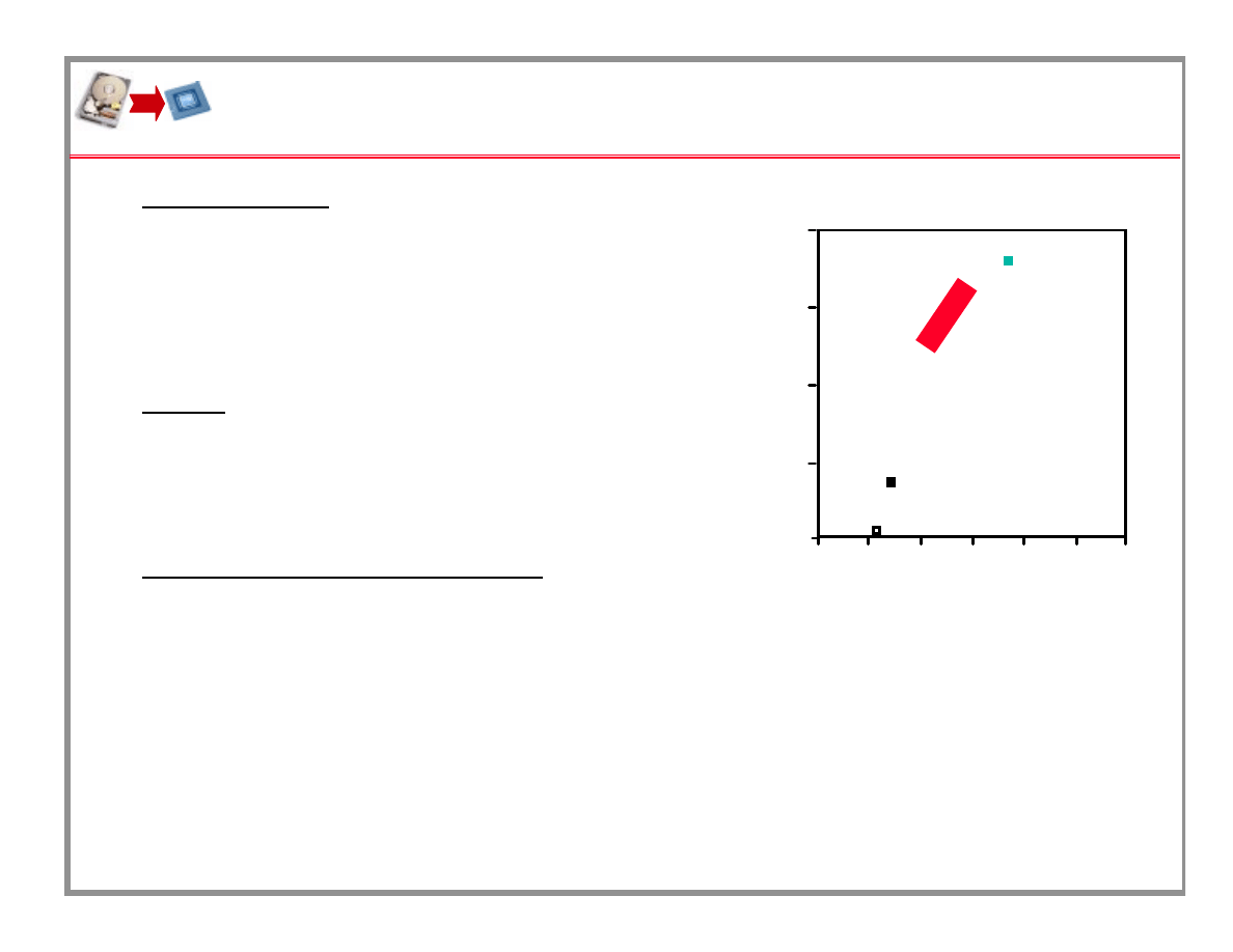
Motive: Lower Data Latency
• Motivation:
– Many types of software limited by access time to data
» Generally when future accesses hard to predict
(e.g., Transactions Based Processing)
– Conventional disk drives limited by rotational velocity:
» at 10,000 RPM worst case rotational latency is about 6ms
» at 30,000 RPM (dental drill speeds!!) still 2ms
– IC-Based Mass Store: latency designable param. - 100’s of µs possible
Worst-Case
Access
Time
Cost $ / GB
$1 / GB
$10 / GB
$100 / GB
$1000 / GB
10ns
1µs
100µs
10ms
DRAM (volatile)
HARD DISK
HI
2
PS
2
Prediction
2005
EEPROM (Flash)

L. R. Carley - “Highly Integrated Information Processing and Storage Systems” page 9 September 1999
&DUQHJLH 0HOORQ
Building the Hardware
• Integration already achieved for CPU, RAM, Comm.
• The Major Challenge: Si-Based Nonvolatile Mass Memory
–
Manufacturing nonvolatile mass memory systems using IC wafer fab
»
Compatibility with IC limits processing temperatures and chemistry
• Existing Approaches to building Si integrated NV RAM
–
Today’s approaches are all based on lithographically defined cells
–
For Example: EEPROM (flash memory) - Block erasable NV RAM
FE-RAM and M-RAM new approaches - direct rewrite NVRAM
–
Whats the problem?: Lithography!! Typical storage cell > 3
λλλλ
x 3
λλλλ
= 9
λλλλ
2
–
Development of lithography with 20nm features FAR in future!!!
• Novel Approach to IC-based rewritable mass storage
–
Disk drives define bit cells by mechanical positioning of head
–
IC-Based equivalent - newly emerging research suggests
»
MEMS-based positioning mechanisms
»
Probe-tip-based reading and writing mechanisms for data storage
(e.g., Scanning Tunneling Microscope - STM, AFM, MFM, etc.)

L. R. Carley - “Highly Integrated Information Processing and Storage Systems” page 10 September 1999
&DUQHJLH 0HOORQ
Probe-Based Storage Mechanisms
• Rewritability and fast write time are critical
– Cache applications may write more often than they read
due to speculative prefetching
• Rewritable storage mechanisms
– Thin-film magnetic recording
» Continuous-film bit size > 20nm dia. marks
(thermal stability limit)
» Tips / write heads are quite difficult to design
» Discrete patterned media could result in smaller marks
– Amorphous / crystaline material (e.g., rewritable CD)
» Requires “thermal” generation
» Tips / write heads / read heads straightforward
» Mark size related to tip and thermal properties - order 3-10nm dia.
– Ferro-electric materials
» Electric field causes transformations
» bv
» Mark size related to tip shape - order 10-20nm dia.

L. R. Carley - “Highly Integrated Information Processing and Storage Systems” page 11 September 1999
&DUQHJLH 0HOORQ
Probe-Based Storage Mechanisms
• Rewritability and fast write time are critical
- Approaches:
– Thin-film magnetic recording
» Continuous-film bit size > 50nm dia. marks
(by thermal stability & SNR)
» Tips / write heads are quite difficult to design
– Amorphous / crystaline material (e.g., rewritable CD)
» Tips / write heads / read heads straightforward - roadblock rewritability
» Mark size related to tip and thermal properties - order 3-10nm dia.
– Ferro-electric materials
» Electric field causes transformations - simple probe tips
» Mark size related to tip shape and media structure - order 10-20nm dia.
» Main roadblock: rewritability and media structure control
– Thermal melting of materials (IBM Almaden / Zurich approach)
» Melt plastic with hot probe tip
» Mark size related to tip shape - order 30-40nm dia.
» Main roadblock: Block erase to re-melt large area
– Charge storage on insulators (like EEPROM)
» Easy to fabricate - big concern is long term charge stability
L. R. Carley - “Highly Integrated Information Processing and Storage Systems” page 12 September 1999
&DUQHJLH 0HOORQ
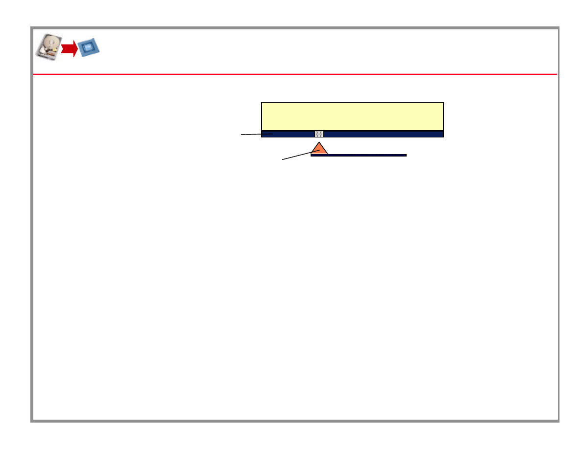
Magnetic Storage
Magnetic Probe tip
Magnetic media
•
Magnetic storage is an attractive choice
– > 1 GB / cm
2
density achievable today
– Reversible (rewritable) - unlimited # of cycles
– Proven to be robust
– Stable
– Most well-understood technology
•
Other possibilities should be explored too
L. R. Carley - “Highly Integrated Information Processing and Storage Systems” page 13 September 1999
&DUQHJLH 0HOORQ
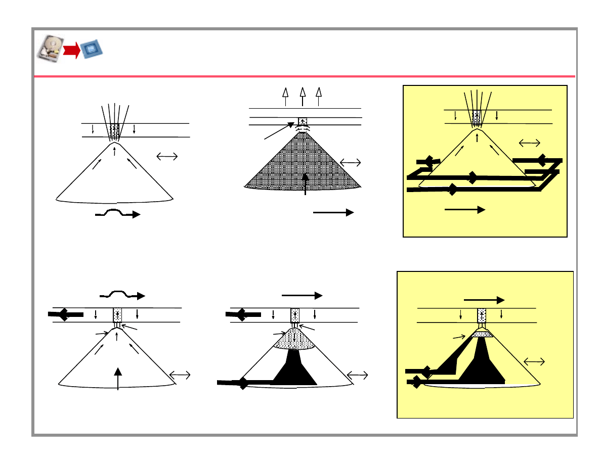
Magnetic Read-Write Mechanisms
• Reading mechanisms:
Soft Tip
Medium
Magnetic Flux
Tip Actuation
Write
Drive Coil
Lines
Current
Medium
Sense
Magnetic Tip
Current
Spin
Tunneling
(electrically
conductive)
Tip
Actuation
Dependent
Current
Medium
Magnetic
Sense
GMR
Current
Sensor
Tip
Actuation
Flux Lines
(soft magnetic tips)
magnetoresistive sensor
spin-dependent tunneling
(requires separate erase head)
• Writing mechanisms:
Hard Tip
Medium
Magnetic Flux
Tip Actuation
Z - motion at bit rate
Lines
hard magnetic tip
Z - motion flat
Medium
Sense Current
Magnetic Tip
Force
(electrically
conductive)
Tip
Actuation
Magnetic
MFM tip / current read
Hard Tip
Z - motion
at bit rate
Z - motion
flat
Z - motion
flat
Metallized
Resistive Medium
External
Tip
Write Current
Magnetic Field
Tunneling Current
Heated
Region
Tip
Actuation
thermo-magnetic writing
Magnetic Medium
Z - motion flat
inductive writing
L. R. Carley - “Highly Integrated Information Processing and Storage Systems” page 14 September 1999
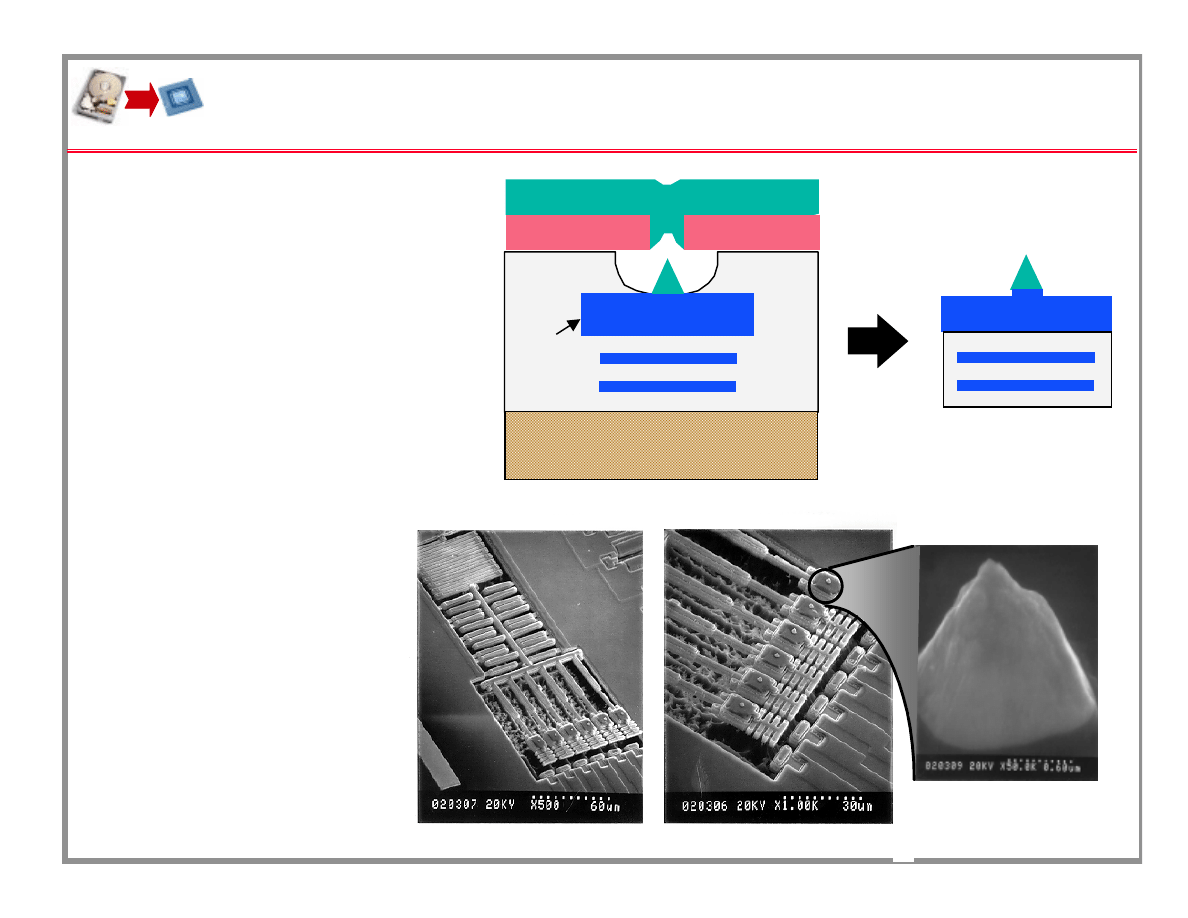
&DUQHJLH 0HOORQ
Example of Tip Fabrication
• Spindt tip process
• Pt Tips survive
post-CMOS
fluorine-based
plasma etches
(could be covered
with resist if
necessary)
• Multiple Pt tips
deposited on a
single CMOS
micromachined
structure
oxide
substrate
Al
Tip Material
resist
L. R. Carley - “Highly Integrated Information Processing and Storage Systems” page 15 September 1999
&DUQHJLH 0HOORQ
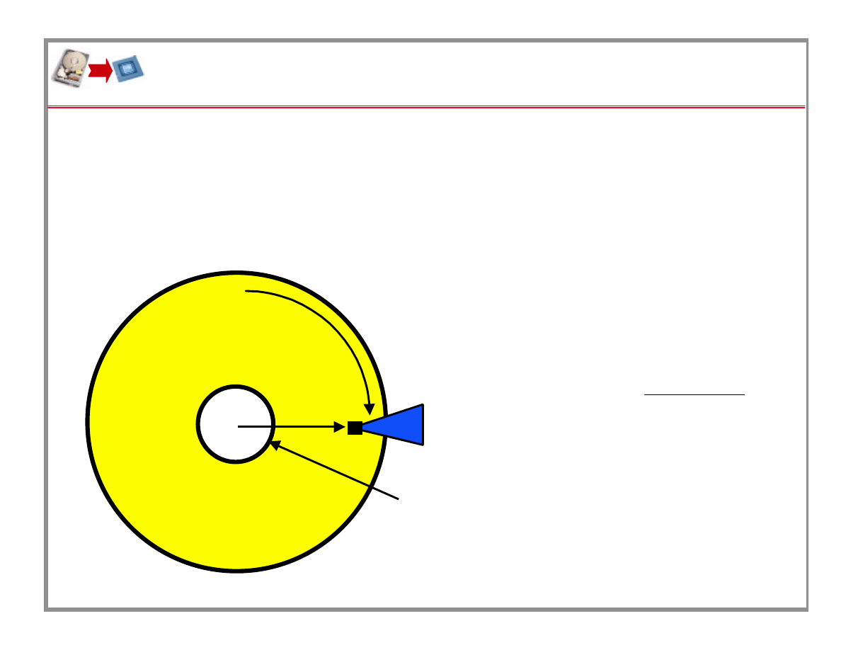
Positioning: The Rotating Disk
• Traditional Approach in Disk Drives
– Theta position provided by rotation
– Radius position controlled by macroscopic magnetic actuator
– Z position (height) controlled by air flow under air bearing surface
R
Velocity = ( 2
ππππ
R ) x RPM / 60
Rotational Latency = 60
2 x RPM
Data Rate = Lin. Density x Velocity
BAD NEWS !!!
- No good bearings
in MEMS Technology
L. R. Carley - “Highly Integrated Information Processing and Storage Systems” page 16 September 1999
&DUQHJLH 0HOORQ
MEMS Actuator Design
• Consider 1D example
• Use “beam” springs
– Avoid friction and contact
– Repeatable and reliable
– K
∝
∝
∝
∝ ((((
f / L)
3
– Decreasing feature size (f) -- f
3
• Use electrostatic actuation
– Easily integrated with electronics
– Electrostatic force, F
∝
∝
∝
∝
L V
2
• High-voltage IC process
– improves force as V
2
• Decreasing IC feature size (f)
– improves force as V
2
L
L
V
P
+
-
V
N
+
-
L. R. Carley - “Highly Integrated Information Processing and Storage Systems” page 17 September 1999
&DUQHJLH 0HOORQ
MEMS Actuator Performance
• Three primary performance measures for actuator
– % swept length (area)
– Seek Time
– Max Operating Shock V = 10V f = 2
µµµµ
m 2
µµµµ
m 1
µµµµ
m
• For 1-D example:( f is feature size)
L= 1mm 0.5mm 0.25mm
• % swept length
≅ ≅
≅ ≅
≅ ≅
≅ ≅
26 % 3.2% 12.5%
ε
ε
ε
ε
οοοο
V
2
L
3
2 E
f
5
• Access time
≅≅≅≅
≅
≅
≅
≅
12ms 2.1ms 1.1ms
E
L
5
ρρρρ
f
3
• Max G Shock
≅
≅
≅
≅
≅
≅
≅
≅
4.6 g 9.2g 37g
(10% force)
ε
ε
ε
ε
οοοο
V
2
1
20
ρρρρ
L
f
2
5

L. R. Carley - “Highly Integrated Information Processing and Storage Systems” page 18 September 1999
&DUQHJLH 0HOORQ
Many Stage Possibilities
• What Moves??
– Move the media in X & Y, move the head in Z
» PRO:
Single media can have single actuator and suspension for
many probe tips -- very high storage density
» CON:
Large media sled is very massive -- long access times and
poor shock resistance
– Move the head in X & Y & Z
» PRO:
Head mass is very small -- fast access times and
excellent shock resistance, many simultaneous accesses possible
» CON:
Swept area limited by single actuator overhead
(probably not better than 1%) -- low storage density
– Compromise: Move the M small media sleds in X & Y, move head in Z
» PRO:
Smooth trade-off between swept area and access time / shock
resistance
» CON:
More complex control systems, fewer simultaneous accesses
L. R. Carley - “Highly Integrated Information Processing and Storage Systems” page 19 September 1999
&DUQHJLH 0HOORQ
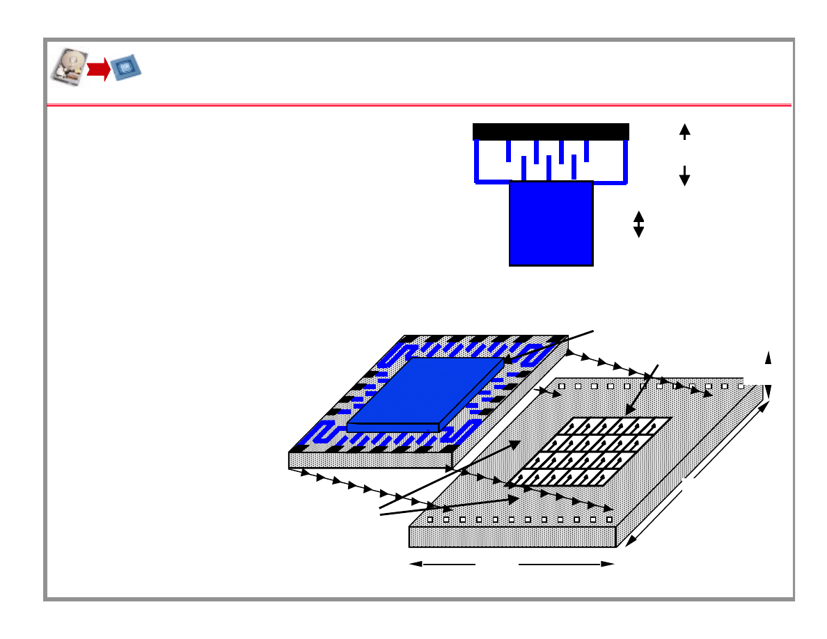
MEMS + Probe-Tip-Based Storage
•
X-Y Translation
– Avoids rotation problem
– No bearings
•
Typical MEMS electrostatic
actuators inefficient
– Many different structures
– Best efficiency 10%
•
Conclusion:
–
Array of Probe Heads
–
Media long
compared to
actuators
•
Large Array of
Probe Heads:
– Media moves by probe tip
pitch in X and Y
Tip
Array
Media
Coating on
Bottom
Surface
1 cm
1 cm
1 mm
Electronics
Media
Sled
Media
Sled
∆∆∆∆
Y < Yo / 10
Yo
Actuator
Size
Media
Motion
Example Device
L. R. Carley - “Highly Integrated Information Processing and Storage Systems” page 20 September 1999
&DUQHJLH 0HOORQ
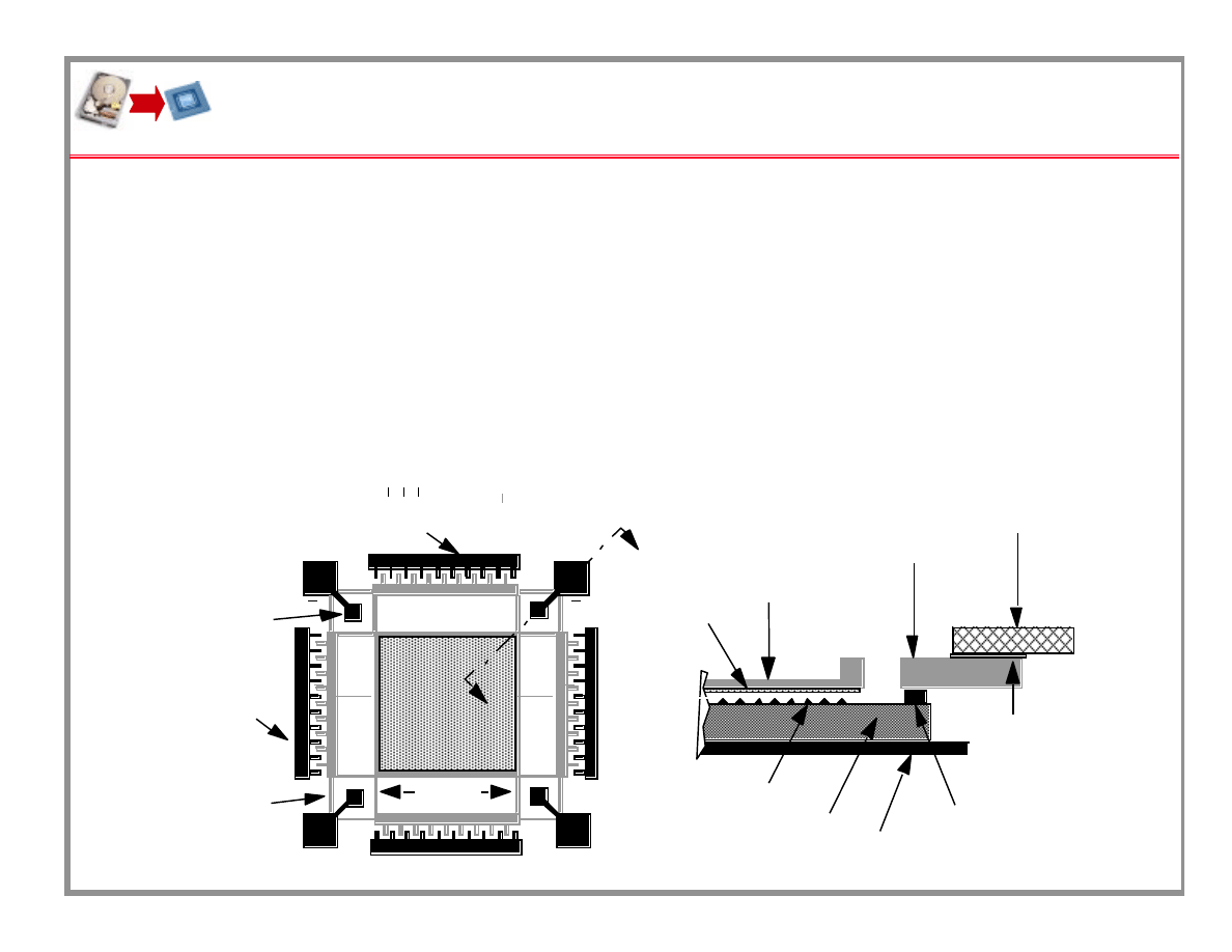
Media Actuator Examples
•
Kionix (Cornell) stage - 4mm x 4mm with 40 µm stroke
•
HP Design Example: 1mm x 1mm media, ±8 µm stroke
2mm x 2mm total size
⇒
⇒
⇒
⇒
25% swept area
–
Hoen et. al., “Electrostatic Surface Drives, …,” Transducers 1997
•
CMU Design - 8 mm x 8 mm media, ±50 µm stroke
14mm x 14mm total size
⇒
⇒
⇒
⇒
32.7% swept area
electrostatic
x actuator
electrostatic
y actuator
beam spring
CMOS chip
standoff
and sensor
media
A’
A
A
A’
CMOS die
moving stage
tip-media
spacer
anchor point
of media stage
handle
wafer
8 mm
oxide
insulating
layer
IC package
tips
media
L. R. Carley - “Highly Integrated Information Processing and Storage Systems” page 21 September 1999
&DUQHJLH 0HOORQ
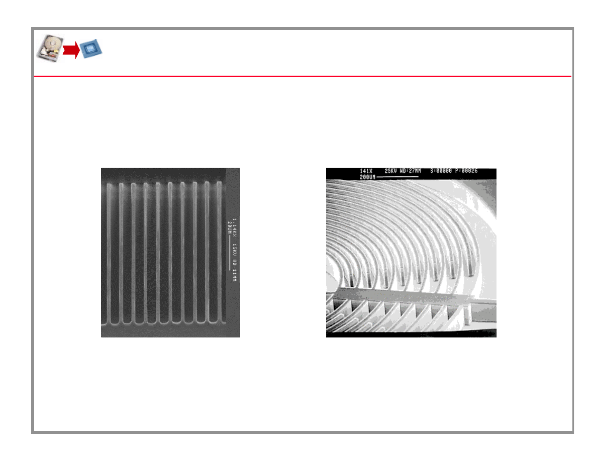
Media Actuator Fabrication
•
High-density ICP process developed by Bosch
•
> 2 µm/min etch rate
•
> 25:1 aspect ratio
Si trenches 80 µm deep,
4.5 µm spaces, 2 µm lines
(STSystems*)
170 µm-deep Si accelerometer;
20 µm features
(Lucas Novasensor*)
* Obtained from http://www.stsystems.com
L. R. Carley - “Highly Integrated Information Processing and Storage Systems” page 22 September 1999
&DUQHJLH 0HOORQ
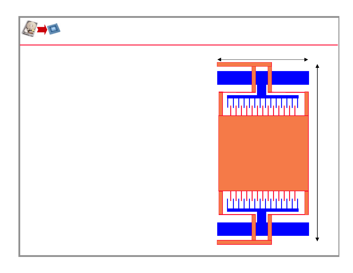
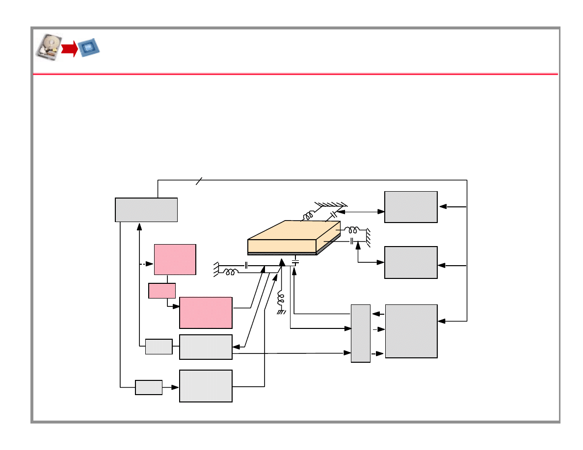
Integration of Circuits with Tips
•
Typical system has large # tips; e.g., 6,400. Each must be:
–
Sensed and servoed in Z and
∆∆∆∆
Y
–
Data must be read and written
–
Too many wires unless some electronics integrated with probe tips
y servo
x servo
tip write
tip read
media
tip
controller
mu
x
track
error
data
address
z servo
tip servo
mux
mux
mux
L. R. Carley - “Highly Integrated Information Processing and Storage Systems” page 23 September 1999
&DUQHJLH 0HOORQ
CMOS High-Aspect-Ratio MEMS
Overglass
3-metal
interconnect
0.5 µm
n-well
CMOS
Gate polysilicon
Silicon
substrate
■
Structures made using conventional CMOS
■
Hewlett-Packard CMOS14 available from MOSIS
■
Construct a beam from CMOS chip:
* G.K. Fedder, et.al., Sensors and Actuators, vol. A57, (1996).
L. R. Carley - “Highly Integrated Information Processing and Storage Systems” page 24 September 1999
&DUQHJLH 0HOORQ
CMOS High-Aspect-Ratio MEMS
Composite
structural layer
Exposed silicon
■
Post-CMOS reactive-ion etch of dielectric layers
■
Top metal layer acts as a mask & protects the CMOS
Via to inner
layers
Metal mask
* G.K. Fedder, et.al., Sensors and Actuators, vol. A57, (1996).

L. R. Carley - “Highly Integrated Information Processing and Storage Systems” page 25 September 1999
&DUQHJLH 0HOORQ
CMOS High-Aspect-Ratio MEMS
" 1.2 µm
~ 5 µm
Composite
beam
Etched pit
Stator
electrodes
Metal
layers
■
Need 1000’s of wires from MEMS/probes to electronics
■
Developed CMOS compatible MEMS process at CMU
■
Post-CMOS etch of silicon substrate
■
Structures are undercut & released
* G.K. Fedder, et.al., Sensors and Actuators, vol. A57, (1996).
L. R. Carley - “Highly Integrated Information Processing and Storage Systems” page 26 September 1999
&DUQHJLH 0HOORQ
CMOS High-Aspect-Ratio MEMS
" 1.2 µm
~ 5 µm
Composite
beam
Etched pit
Stator
electrodes
Metal
layers
■
Need 1000’s of wires from MEMS/probes to electronics
■
Developed CMOS compatible MEMS process at CMU
■
Post-CMOS etch of silicon substrate
■
Structures are undercut & released
* G.K. Fedder, et.al., Sensors and Actuators, vol. A57, (1996).
L. R. Carley - “Highly Integrated Information Processing and Storage Systems” page 27 September 1999
&DUQHJLH 0HOORQ
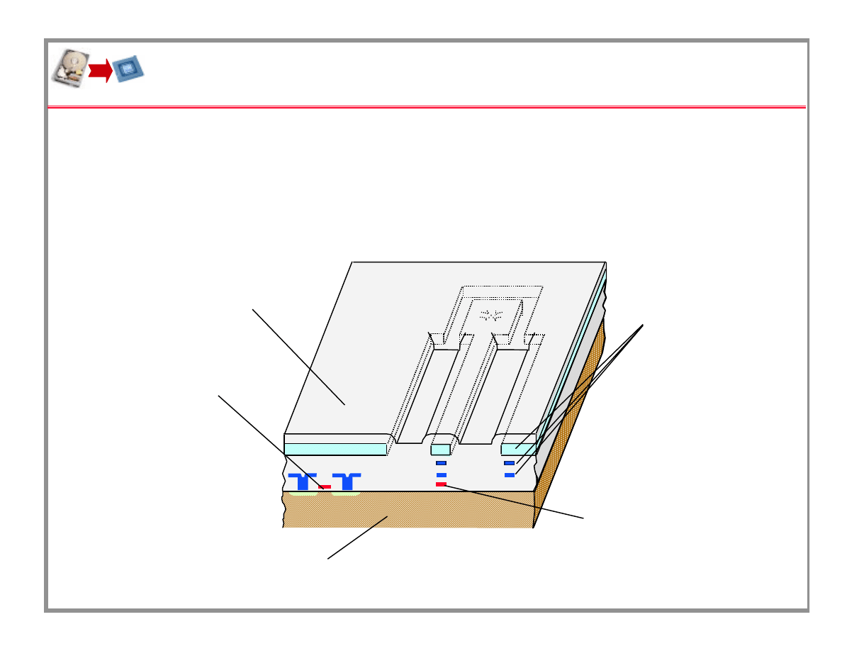
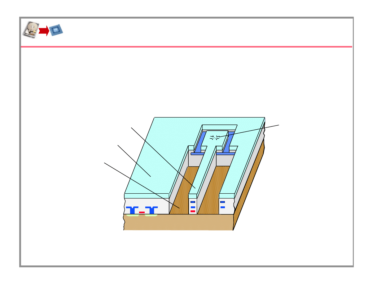
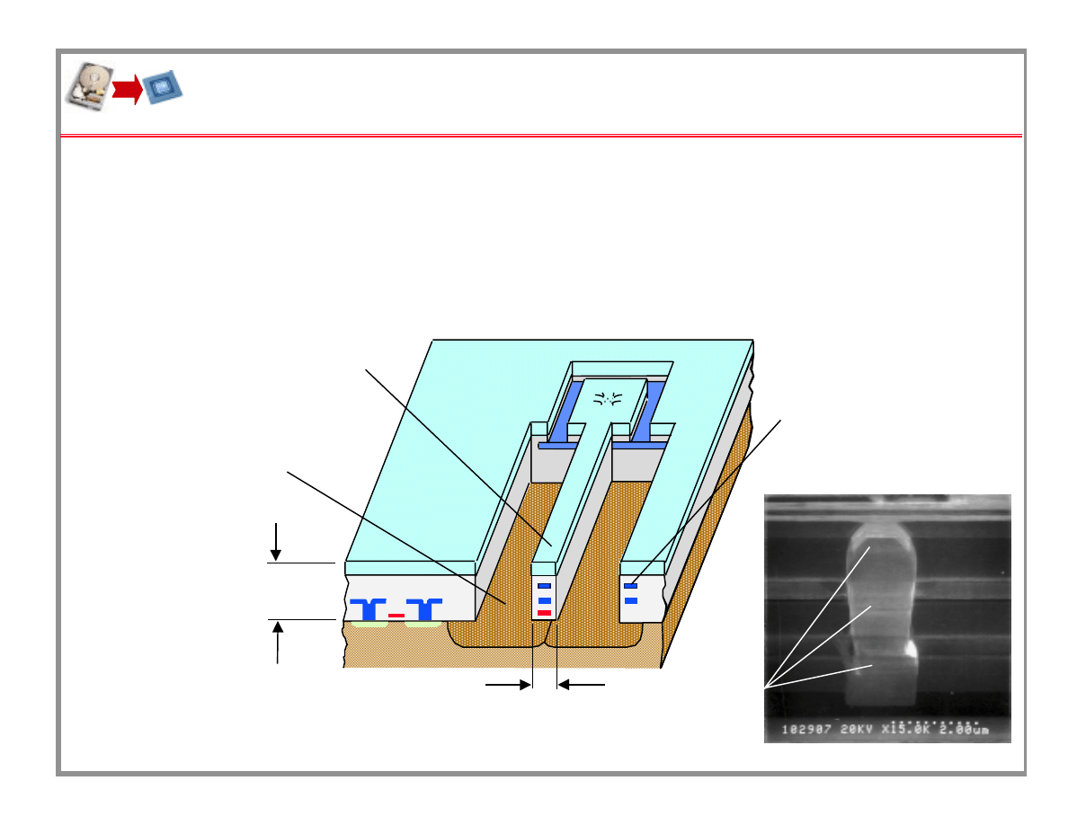
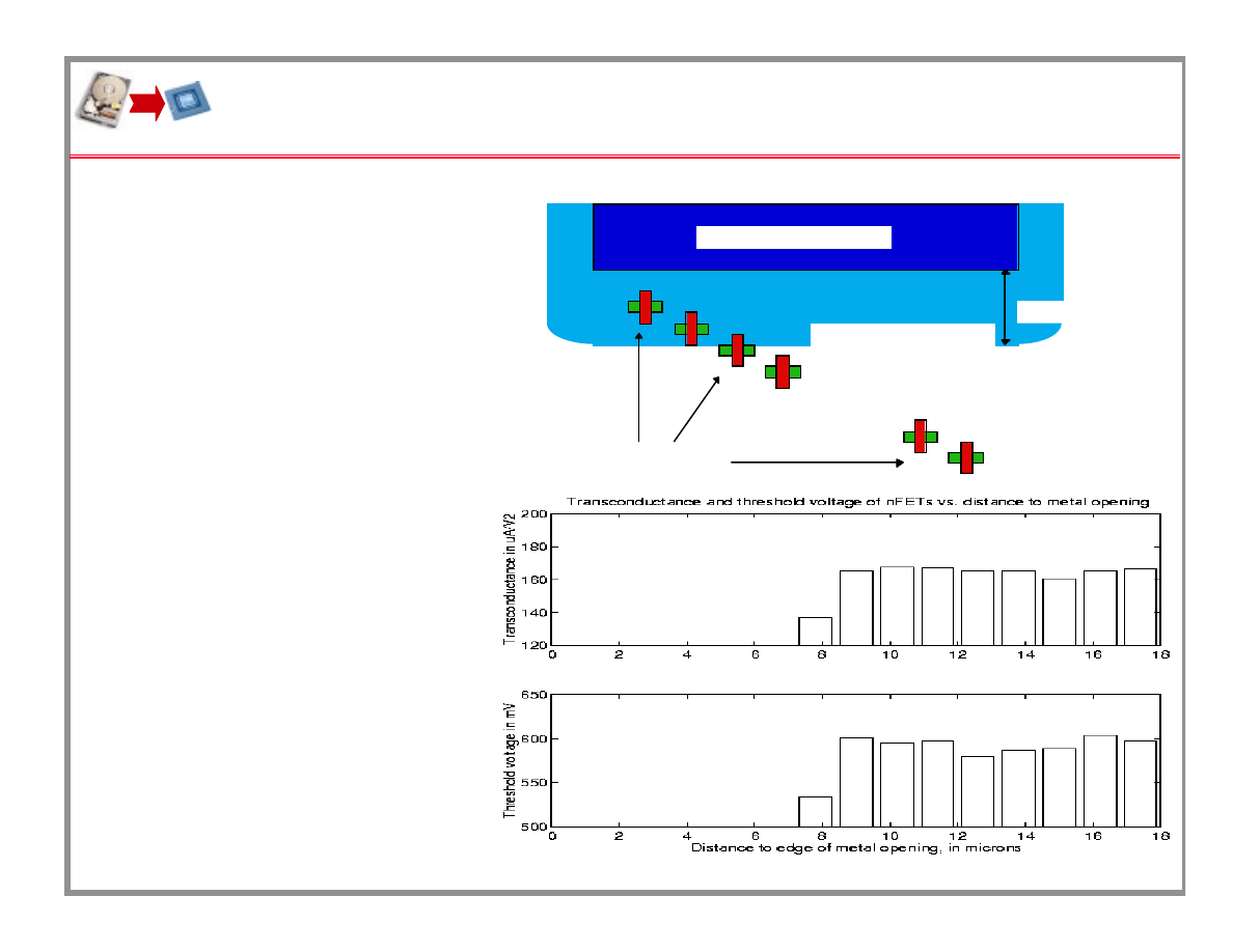
FETs and Circuits on MEMS Chip
• Isotropic silicon
etch required to
release MEMS
structures
• FETs closer than
8 µm are etched
away
• Beyond 8 µm,
FETs’ gain and
threshold are not
affected
• No degradation
after 4 months
7um
. . . . . .
12 test FETs
actual edge of etched pit
metal opening for etching
L. R. Carley - “Highly Integrated Information Processing and Storage Systems” page 28 September 1999
&DUQHJLH 0HOORQ
Example of Z Probe Tip Actuator
• Z suspension needed
for every Probe Tip
– surface roughness
– surface curvature
– tip height variations
• IBM Zurich - AFM tip array
– 32 x 32 array of probe tips
– Despont et. al., MEMS ‘99
• Alternative: active Z actuation
parallel-plate metal-to-media
– Allows active spacing
– Does not require contact
• Small Lateral Deflection
– Thermal expansion mismatch
• CMU Design Example
spring
suspension
structure length = 231 µm,
beam width = 1.8 µm,
comb gap = 1.8 µm
lateral
comb actuator
vertical
actuator
probe tip
pad

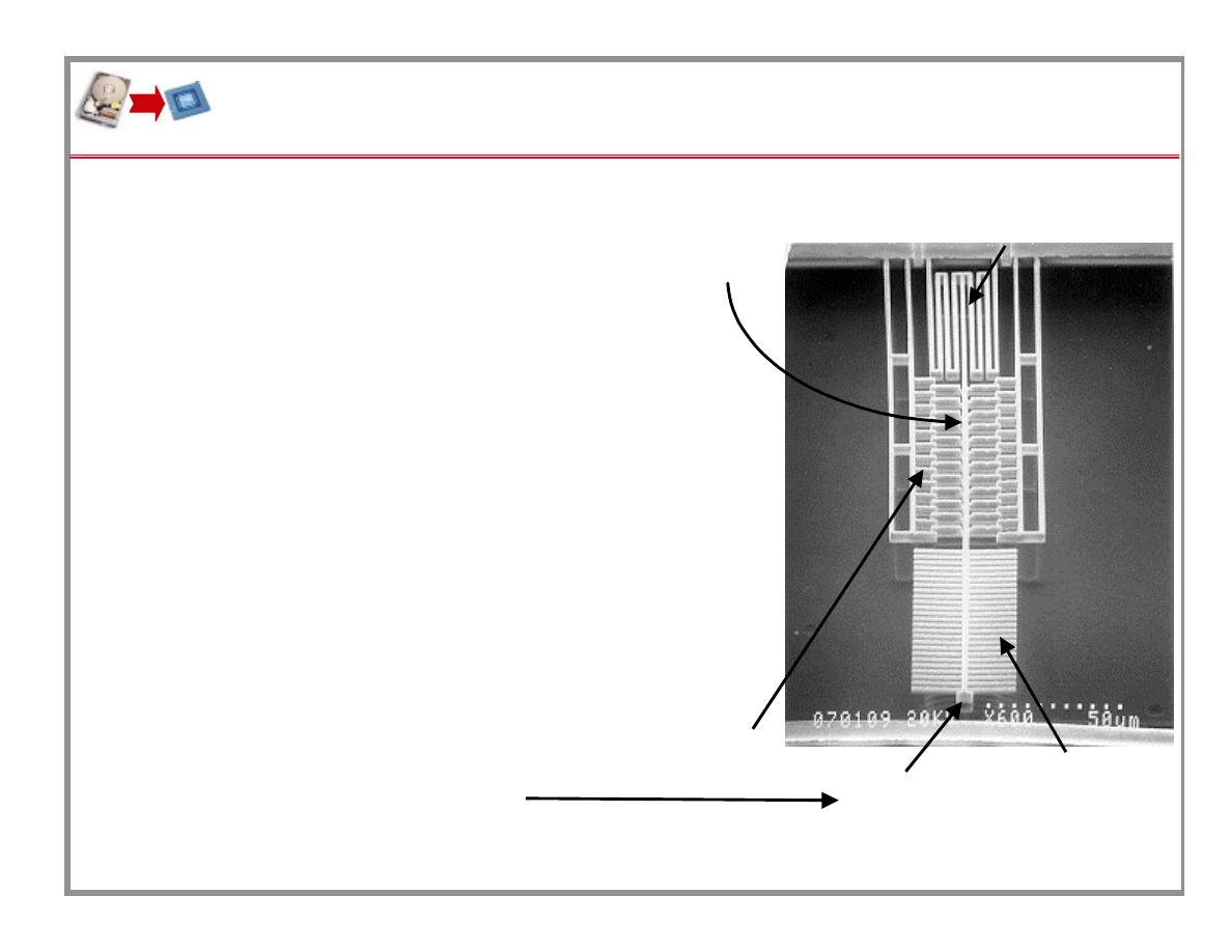
L. R. Carley - “Highly Integrated Information Processing and Storage Systems” page 29 September 1999
&DUQHJLH 0HOORQ
New Degrees of Freedom
• Hopefully, convinced IC-based mass storage possible
– Will require focussed research to make it practical
• IC-Based storage has many degrees of freedom; e.g.,
– What is storage mechanism - magnetic is best candidate so far?
– How are reading and writing performed?
– How many probe tips on a single MEMS Z-suspension?
– How many probe tips per MEMS media sled?
– How many instances of detection and positioning electronics?
– How many media sleds / IC?
– Is processing integrated with storage subsystems?
If so, what is the best pattern for interconnection?
– What kind of processors should be integrated with storage subsystems?
Traditional DSPs vs. VLIWs vs. FPGAs vs. something new?
• Understand applications to make informed trade-offs
– We need to study and understand broad application classes
– We need simulation model to relate application needs to design choices
L. R. Carley - “Highly Integrated Information Processing and Storage Systems” page 30 September 1999
&DUQHJLH 0HOORQ
Parallelism of Tips for Data Rate
• Example of Decision -- pattern for reading and writing
– More tips active more data rate and more power dissipation
– Cannot access independent locations with tips on same media sled
0
1
2
3
4
5
6
7
8
9
79
0
1
2
3
79
Read from all
tips in the
row in parallel.
80 bits per
read cycle
1
1
1
1
1
1
1
1
1
1
1
L. R. Carley - “Highly Integrated Information Processing and Storage Systems” page 31 September 1999
&DUQHJLH 0HOORQ
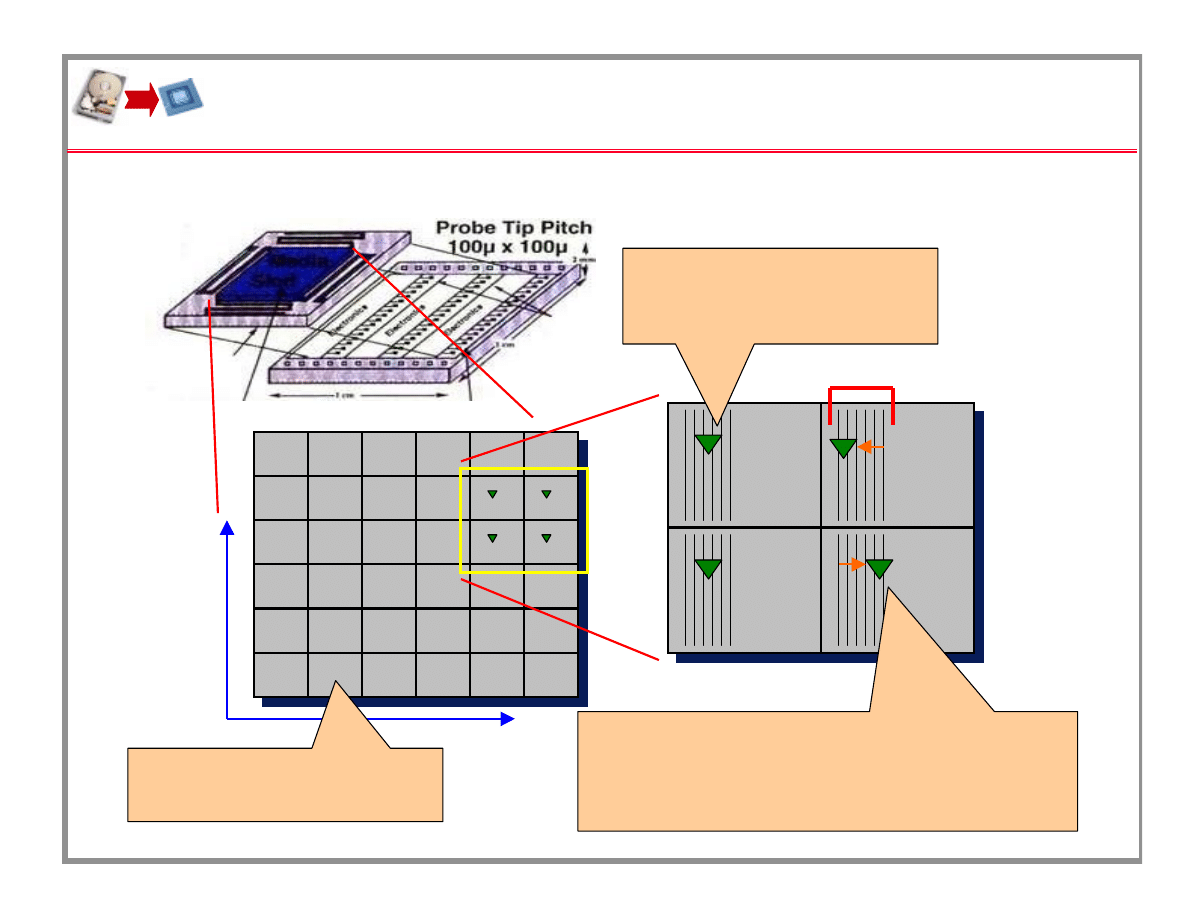
Data Assignment Decisions
• Another degree of freedom is how to map data to device
The media sled moves in
X and Y above the tip array.
Y
X
Tips are fixed so they each
are positioned over the same
track group in each square.
However, each tip has some
freedom to move in the X direction
so they can
deflect +/- 5 tracks within
a track group, independent of the other tips.
Track Group
L. R. Carley - “Highly Integrated Information Processing and Storage Systems” page 32 September 1999
&DUQHJLH 0HOORQ
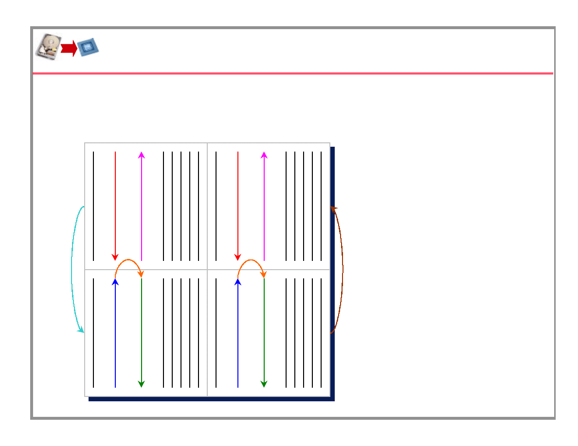
Example Data Access Pattern
• Even choices to make for how to scan sled across data
– And, these choices all make a difference to application performance
1)
Tips in row 1 read down
to end of track 2.
2)
Tip switch - row 2 tips
turn on.
3)
Tips in row 2 read up to
end of track 2.
4)
Sled seeks to next
track.
5)
Tips in row 2 read down
to end of track 3.
6)
Tip switch - row 1 tips
turn on.
7)
Tips in row 1 read up to
end of track 3.
1)
1)
2)
3)
3)
4)
4)
5)
5)
6)
7)
7)

L. R. Carley - “Highly Integrated Information Processing and Storage Systems” page 33 September 1999
&DUQHJLH 0HOORQ
Exploration Via System Simulation
• Created Processor+Storage System Model using SimOS
– Work of Professors Nagle and Ganger and their students
– Implemented a simple MEMS model based on original SimOS disk model.
– Implemented a new SimOS disk model using DiskSim.
– Re-implement a detailed MEMS model as a module in DiskSim.
• Resimulate System Performance
with different MEMS Storage System parameters
– Can see application-level impact of changes in basic science
– For example,
» Physicist working on new head/media combination with
higher density but longer write time can see impact on system
• This overall flow of information is at core of center idea
– Basic Science
→
→
→
→
Storage subsystem designer
→
→
→
→
Technology
– Technology + architectural decisions
→
→
→
→
proposed new system
– Proposed new system + simulation
→
→
→
→
feedback to all levels

L. R. Carley - “Highly Integrated Information Processing and Storage Systems” page 34 September 1999
&DUQHJLH 0HOORQ
Example Simulation Results
•
Capacity
–
2.56 GB per cm
2
with 1 media actuator with 1cm x 1cm sled
(about the worst possible seek time case)
•
Latency
–
Tip actuator takes 5 ms to 0.1 ms to seek
»
Compare to 12 ms to 0.6 ms for Seagate Cheetah Disk
–
MEMS tip actuator can read from ±5 tracks without media seek
–
MEMS Media sled inertia dominated - 1 to 10 ms extra latency
exact motion can be predicated given a maximum actuator force
•
Data Rate
–
Assume Probe Tip recording at 200 kb/s per tip
–
100 to 10,000 simultaneous tips depending on power dissipation limits
–
2Gb/s maximum possible for 1 cm
2
device
•
Power
–
Dominated by number of active tips
–
Assume 5 mW / active tip + 100mW for media positioner
L. R. Carley - “Highly Integrated Information Processing and Storage Systems” page 35 September 1999
&DUQHJLH 0HOORQ
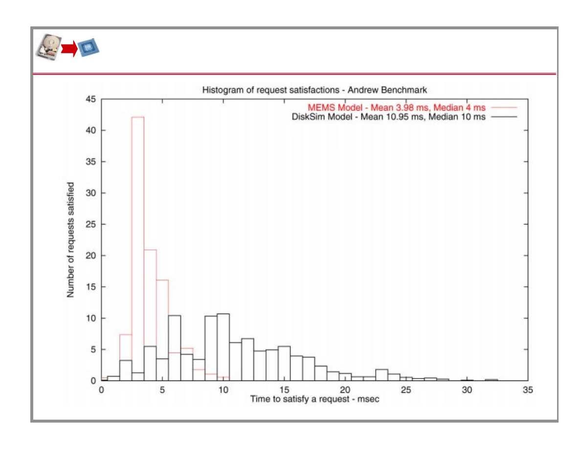
Example (1): File Server
L. R. Carley - “Highly Integrated Information Processing and Storage Systems” page 36 September 1999
&DUQHJLH 0HOORQ
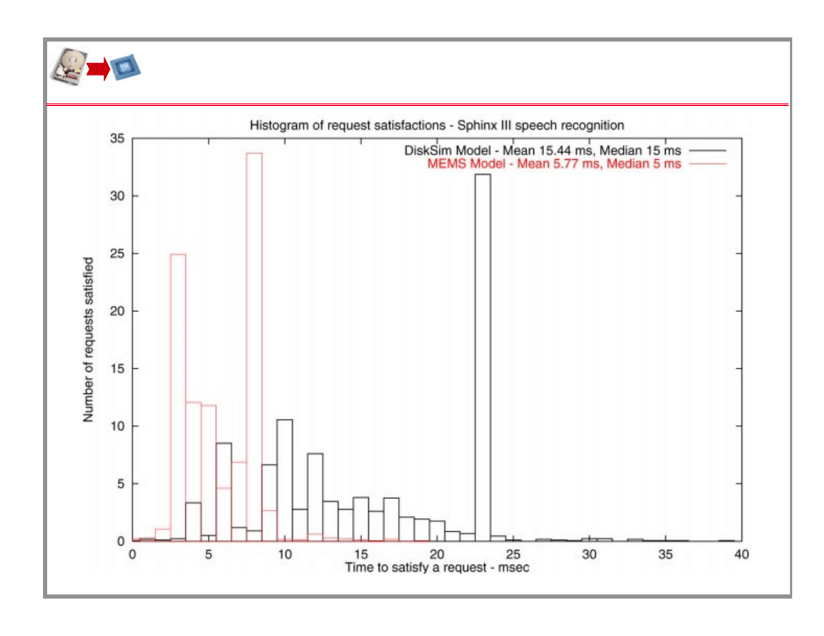
Example (2): Speech Recognition

L. R. Carley - “Highly Integrated Information Processing and Storage Systems” page 37 September 1999
&DUQHJLH 0HOORQ
IC-Compatible CPU +Mass Storage
• IC-Based Data Storage is Achievable
– Lithographically defined approaches already commercially viable
» EEPROM, FeRAM, MRAM (coming soon)
» Storage capacity limited by photolithographic resolution
– X-Y-Z actuation with CMOS IC compatible MEMS
» Demonstrated small swept area
» Much research needed to increase swept area
– Demonstrated simple STM tip fabrication
» Need to develop process compatible magnetic “head” designs
– Demonstrated simple carbon film WORM media
» Need to develop process compatible magnetic media designs
– System Demonstrations
» Need to integrate components with electronics into system demos
» Currently working on a basic Z-only MEMS magnetic probe demo
• Why Do It ??
– Remember Advantages of IC-Based Computing + Storage Systems
» Low Cost, Short Access Time, Low Volume and Mass,
» Potential for Archivability of Data / Software / Hardware
Wyszukiwarka
Podobne podstrony:
Positron emission tomography slides
jj slides tex
credit slides 1
slides01
Thyroid benign slides
Criando Bons Slides
Munsell Slides
Chaos Deterministyczny p19 slides
Vision Slides
Criando Slides
lecture slides 05
Electrocardiograms slides
hai burden slides notes 2002
ZW Pol pien PP 2011 2012 odcinek 1 dla studentów slides z wykładów w dniach 02 16 10 2011
lecture slides
więcej podobnych podstron