
24 lutego 2010
Wojciech Kucewicz
1

Design for
Design for
Design for
Design for
Design for
Design for
Manufacturability
Manufacturability
Design for
Design for
Manufacturability
Manufacturability
Manufacturability
Manufacturability
Manufacturability
Manufacturability
24 lutego 2010
Wojciech Kucewicz
2
From presentation of prof.Wieław Kuźmicz on MIXDES 2003

Design for Manufacturability
Design for Manufacturability
Design for Manufacturability
Design for Manufacturability
Design for Manufacturability:
Design for Manufacturability:
what is it?
what is it?
24 lutego 2010
Wojciech Kucewicz
3
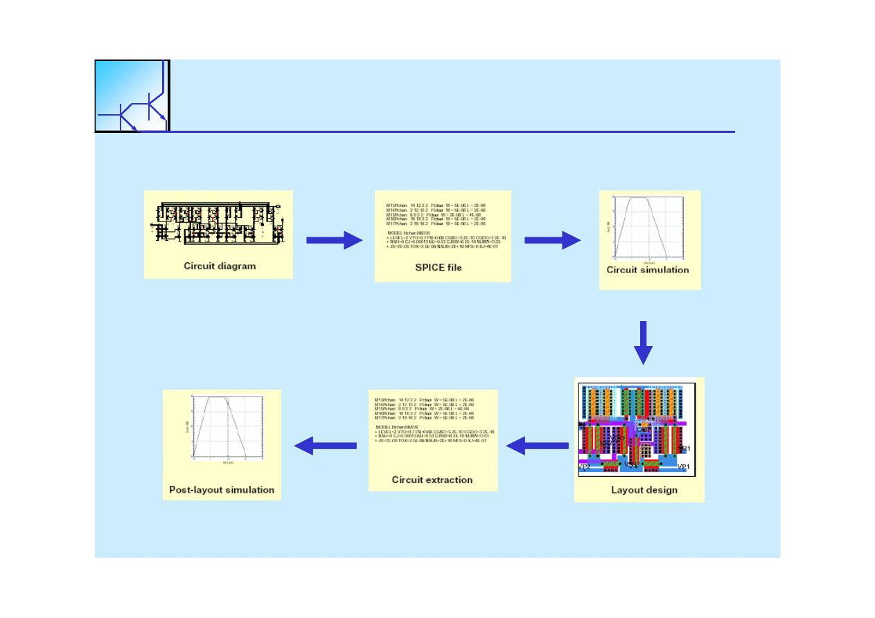
Typical analog IC design cycle
Typical analog IC design cycle
Typical analog IC design cycle
Typical analog IC design cycle
24 lutego 2010
Wojciech Kucewicz
4
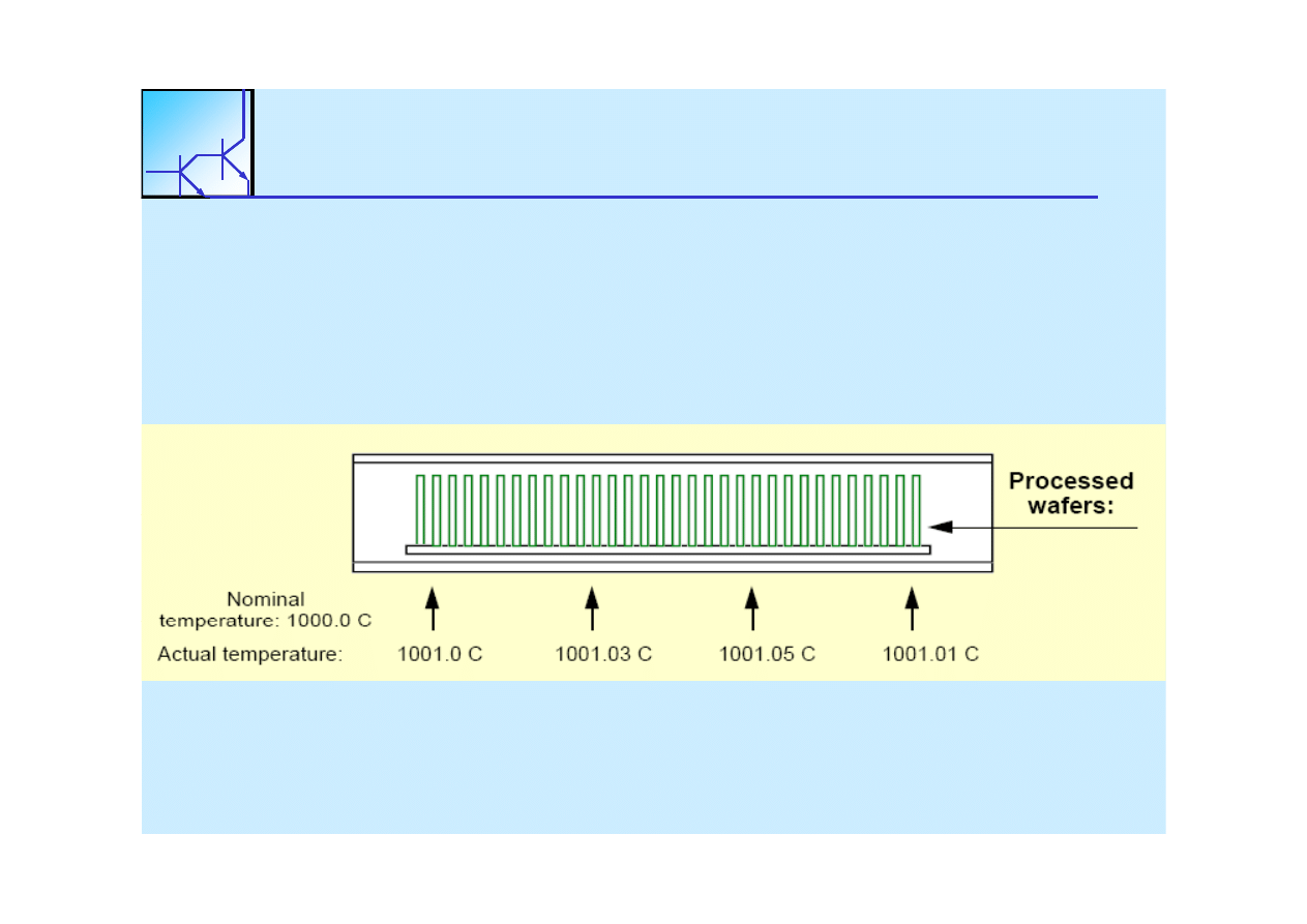
Real circuits exhibit statis
Real circuits exhibit statistical
tical spread of
spread of
parameters and characteristics
parameters and characteristics
Real circuits exhibit statis
Real circuits exhibit statistical
tical spread of
spread of
parameters and characteristics
parameters and characteristics
Acceptance
Acceptance
Acceptance
Acceptance
region
region
This circuit is
This circuit is
not
not
manufacturable
manufacturable
24 lutego 2010
Wojciech Kucewicz
5
This circuit is
This circuit is
not
not
manufacturable
manufacturable
Real circuits exhibit statis
Real circuits exhibit statistical
tical spread of
spread of
parameters and characteristics
parameters and characteristics
Real circuits exhibit statis
Real circuits exhibit statistical
tical spread of
spread of
parameters and characteristics
parameters and characteristics
Acceptance
Acceptance
Acceptance
Acceptance
region
region
This circuit is manufacturable
This circuit is manufacturable
24 lutego 2010
Wojciech Kucewicz
6
This circuit is manufacturable
This circuit is manufacturable

Design for Manufacturability
Design for Manufacturability
Design for Manufacturability
Design for Manufacturability
The question is:
The question is:
H
How to ensure that our design is not
ow to ensure that our design is not only
only
H
How to ensure that our design is not
ow to ensure that our design is not only
only
formally correct, but also
formally correct, but also manufacturable ?
manufacturable ?
The answer is in
The answer is in
Design for Manufacturability
Design for Manufacturability
24 lutego 2010
Wojciech Kucewicz
7

Verification of manufacturability
Verification of manufacturability
Verification of manufacturability
Verification of manufacturability
Formal and functional verification: logic and/or
Formal and functional verification: logic and/or electrical
electrical
Formal and functional verification: logic and/or
Formal and functional verification: logic and/or electrical
electrical
simulations, DRC, LVS.
simulations, DRC, LVS.
Verification and optimization with respect of
Verification and optimization with respect of
Verification and optimization with respect of
Verification and optimization with respect of
secondary/parasitic effects
secondary/parasitic effects
: thermal effects,
: thermal effects, noise, RF
noise, RF
stability, transmission effects in
stability, transmission effects in interconnections etc.
interconnections etc.
yy
Verification and minimization of sensitivity to
Verification and minimization of sensitivity to
manufacturing imperfections
manufacturing imperfections --> reduction of
> reduction of yield losses
yield losses
manufactur ng mp rf ct ons
manufactur ng mp rf ct ons r uct on of
r uct on of y
oss s
y
oss s
due to
due to
catastrophic and parametric
catastrophic and parametric faults
faults
..
24 lutego 2010
Wojciech Kucewicz
8
SOI detektor
SOI detektor
SOI detektor
SOI detektor
SOI Detector 48x48 cells
SOI Detector 48x48 cells
-- yields 20%
yields 20%
24 lutego 2010
Wojciech Kucewicz
9
SOI Detector 128x128 cells
SOI Detector 128x128 cells -- yields 0%
yields 0%

Terminology
Terminology
Terminology
Terminology
D f t
D f t (d f kt t k )
(d f kt t k )
•
•
Defect
Defect (defekt, usterka)
(defekt, usterka)::
a significant difference between designed and
a significant difference between designed and actual IC
actual IC
structure
structure
• Fault
• Fault (wada)
(wada): :
unacceptable IC performance
unacceptable IC performance
24 lutego 2010
Wojciech Kucewicz
10

Design for Manufacturability
Design for Manufacturability
Design for Manufacturability
Design for Manufacturability
Defects:
Defects:
Structural defects:
Structural defects:
breaks, shorts,
breaks, shorts, pinholes etc.
pinholes etc.
Statistical variations of device stru
Statistical variations of device struct
cture
ure
:: doping profiles, layer
doping profiles, layer
thicknesses etc
thicknesses etc
thicknesses etc.
thicknesses etc.
Faults:
Faults:
Catastrophic (hard) faults
Catastrophic (hard) faults
: IC does not
: IC does not work (does not perform its
work (does not perform its
function)
function)
Parametric (soft) faults
Parametric (soft) faults
: IC does work
: IC does work but its performance is
but its performance is
unacceptable
unacceptable
24 lutego 2010
Wojciech Kucewicz
11
unacceptable
unacceptable
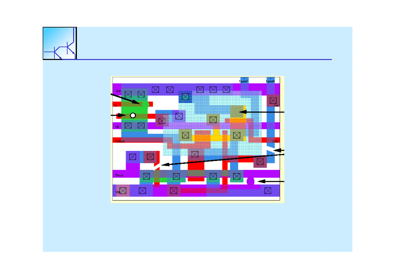
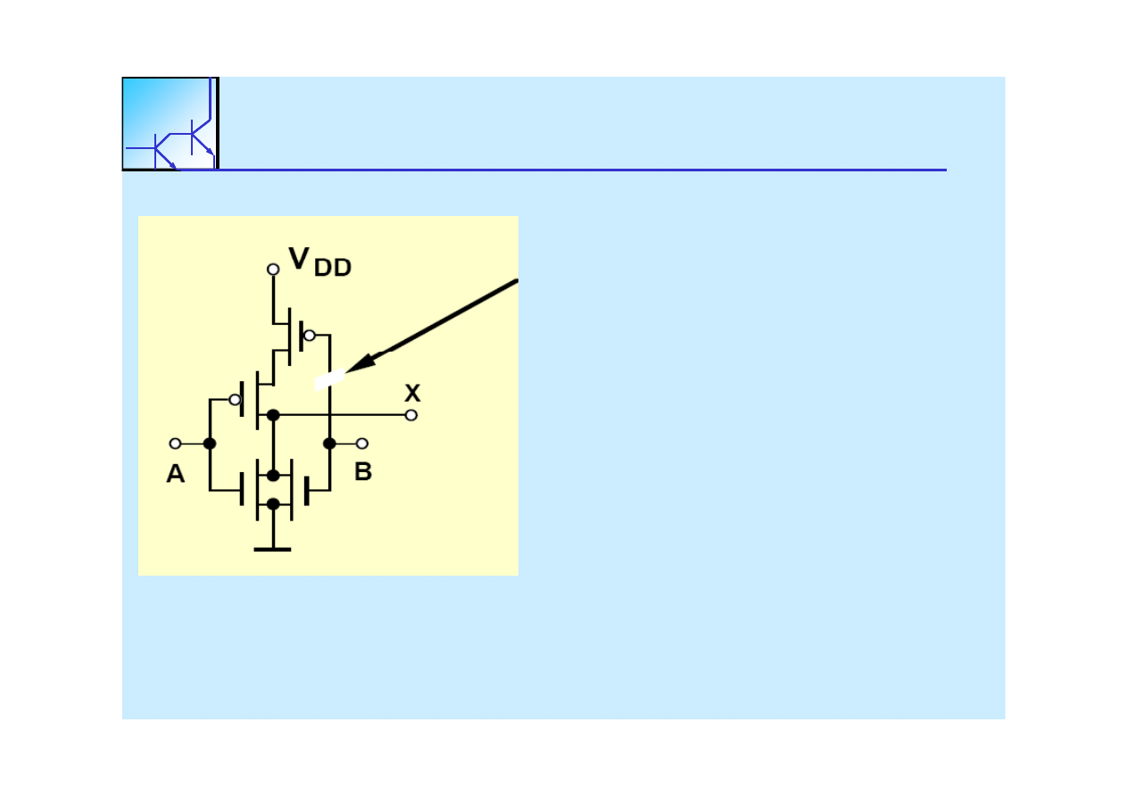
Structural defects
Structural defects
Structural defects
Structural defects
Missing
Missing poly
poly
VDD
VDD
Missing
Missing poly
poly
An oxide
An oxide pinhole
pinhole
A break
A break
(missing
(missing
VDD
VDD
In
In
Out
Out
A break
A break
(
lit
(
lit
(missing
(missing
contact)
contact)
A short
A short (bridge)
(bridge)
(open, split
(open, split
node)
node)
VSS
VSS
St
t
l d f t ft
lt i
t t
hi f lt b t
l
St
t
l d f t ft
lt i
t t
hi f lt b t
l
VSS
VSS
24 lutego 2010
Wojciech Kucewicz
12
Structural defects often result in catastrophic faults but may also
Structural defects often result in catastrophic faults but may also
affect performance
affect performance
Structural defects
Structural defects
Structural defects
Structural defects
A spot of missing metal
A spot of missing metal between
between
two contacts
two contacts results in a break
results in a break
two contacts
two contacts results in a break...
results in a break...
... but not always !
... but not always !
redundant routing
redundant routing
similar shape of
similar shape of the active
the active
area mask
area mask with a similar
with a similar
defect
defect does result in a break !
does result in a break !
24 lutego 2010
Wojciech Kucewicz
13
Structural defects not always result in faults
Structural defects not always result in faults
Design for Manufacturability
Design for Manufacturability
Design for Manufacturability
Design for Manufacturability
In a CMOS circuit voltage on a disconnected
In a CMOS circuit voltage on a disconnected
gg
transistor gate is unpredictable
transistor gate is unpredictable
(a) Low voltage (
(a) Low voltage (~~0) :
0) :
PMOS transistor conducting logic function
PMOS transistor conducting logic function not
not
PMOS transistor conducting, logic function
PMOS transistor conducting, logic function not
not
affected, but:
affected, but: -- increased "0" level and static DC
increased "0" level and static DC
current
current when A = "0", B ="1„
when A = "0", B ="1„ -- speed may be
speed may be
reduced
reduced
(b) High voltage (
(b) High voltage (~~VDD) :
VDD) : PMOS transistor cut
PMOS transistor cut
off, logic output incorrect
off, logic output incorrect when B = "0".
when B = "0".
Consequences of structural defects may be unpredictable
Consequences of structural defects may be unpredictable Structural
Structural
24 lutego 2010
Wojciech Kucewicz
14
q
y
p
q
y
p
defects may result in parametric faults
defects may result in parametric faults Faults are not always easily
Faults are not always easily
observable
observable
Process and layout variations
Process and layout variations
Process and layout variations
Process and layout variations
• Unavoidable disturbances in
• Unavoidable disturbances in
Unavoidable disturbances in
Unavoidable disturbances in
process parameters
process parameters (temperatures,
(temperatures,
times, doses
times, doses etc.)
etc.)
• Unavoidable disturbances in
• Unavoidable disturbances in
Unavoidable disturbances in
Unavoidable disturbances in
litography
litography (under/overetching,
(under/overetching, mask
mask
misalignment, shape
misalignment, shape distortion etc.)
distortion etc.)
• Result: statistical spread of
• Result: statistical spread of device
device
parameters
parameters
parameters
parameters
Th
i ti
l d
t
t i
f lt
b t
Th
i ti
l d
t
t i
f lt
b t t t
hi
t t
hi
24 lutego 2010
Wojciech Kucewicz
15
These variations may lead to parametric faults but
These variations may lead to parametric faults but catastrophic
catastrophic
faults (non
faults (non--functional circuits) are also possible
functional circuits) are also possible
Process variations:
Process variations: classification
classification
Process variations:
Process variations: classification
classification
Global variations: affect all structures in a wafer in the same way,
Global variations: affect all structures in a wafer in the same way,
do
do not introduce mismatch (example: variation of temperature along
not introduce mismatch (example: variation of temperature along
do
do not introduce mismatch (example: variation of temperature along
not introduce mismatch (example: variation of temperature along
aa furnace during thermal processes).
furnace during thermal processes).
Global process variations may result in large
Global process variations may result in large variations of device
variations of device
24 lutego 2010
Wojciech Kucewicz
16
Global process variations may result in large
Global process variations may result in large variations of device
variations of device
parameters
parameters
Process variations:
Process variations: classification
classification
Process variations:
Process variations: classification
classification
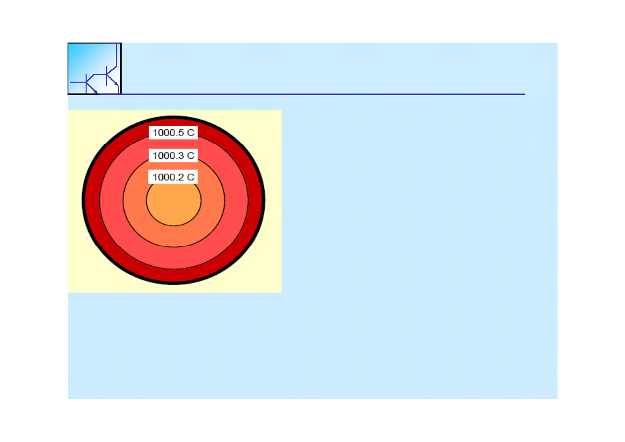
Local deterministic variations are
Local deterministic variations are
Local deterministic variations are
Local deterministic variations are
deterministic (often, but not
deterministic (often, but not always, radial)
always, radial)
functions of position
functions of position on wafer (example:
on wafer (example:
radial variation
radial variation of temperature during
of temperature during
th
l
th
l
ss s)
ss s)
thermal
thermal processes).
processes).
Local deterministic variations introduce mismatch (difference in
Local deterministic variations introduce mismatch (difference in
parameters of identical devices) which increases with distance
parameters of identical devices) which increases with distance
b t
t h d i f
d i
b t
t h d i f
d i
24 lutego 2010
Wojciech Kucewicz
17
between matched pair of devices
between matched pair of devices
Process variations:
Process variations: classification
classification
Process variations:
Process variations: classification
classification
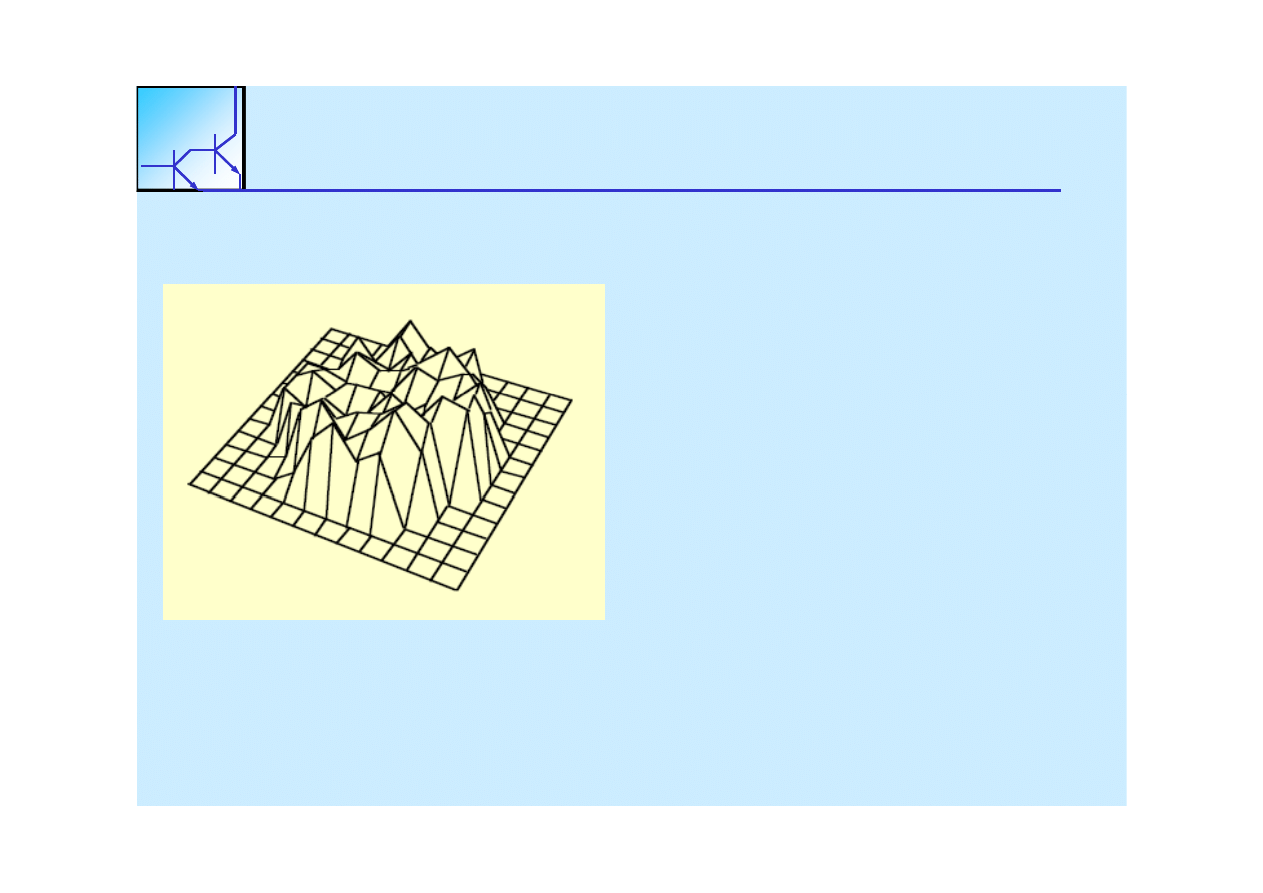
Local random variations: "random
Local random variations: "random noise" in
noise" in
m
m
m
m
some process parameters
some process parameters or material
or material
properties. Example:
properties. Example: random variations in
random variations in
substrate
substrate doping concentration; another
doping concentration; another
example: random variations in carrier
example: random variations in carrier
example: random variations in carrier
example: random variations in carrier
lifetime.
lifetime.
Local random variations introduce mismatch which may or
Local random variations introduce mismatch which may or may not
may not
24 lutego 2010
Wojciech Kucewicz
18
Local random variations introduce mismatch which may or
Local random variations introduce mismatch which may or may not
may not
depend on distance.
depend on distance.
Process variations: classification
Process variations: classification
Process variations: classification
Process variations: classification
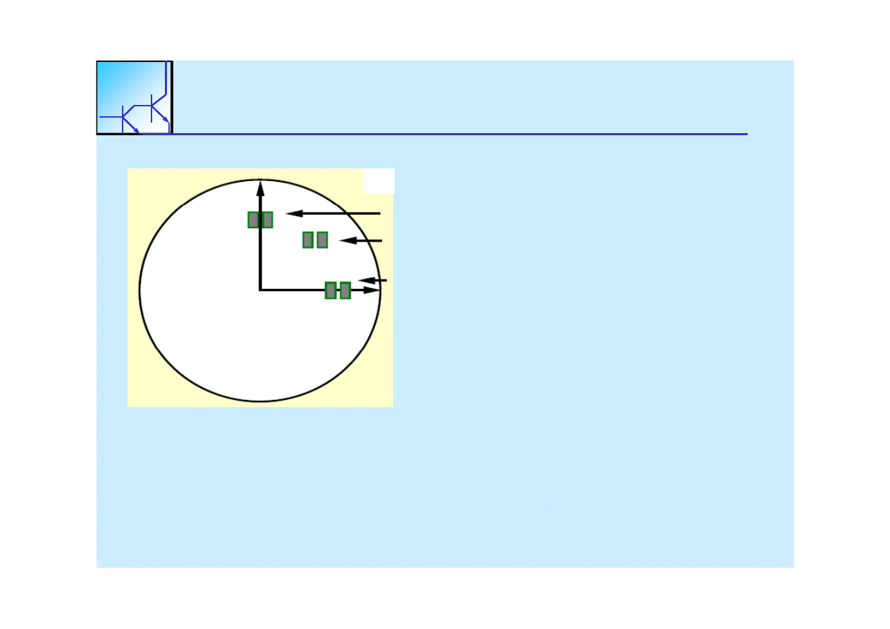
Let's assume radial dependence of V
Let's assume radial dependence of V
T
T
::
No V
No V
T
T
mismatch for this pair of devices
mismatch for this pair of devices
Moderate V
Moderate V
T
T
mismatch for this pair of devices
mismatch for this pair of devices
Large V
Large V mismatch for this pair of devices
mismatch for this pair of devices
Large V
Large V
T
T
mismatch for this pair of devices
mismatch for this pair of devices
For a randomly selected sample of devices coming from
For a randomly selected sample of devices coming from various
various
unknown locations on the wafer deterministic
unknown locations on the wafer deterministic variations seem to be
variations seem to be
24 lutego 2010
Wojciech Kucewicz
19
random !
random ! -- that’s why all local variations
that’s why all local variations are often considered
are often considered
random.
random.
Process variations: classification
Process variations: classification
Process variations: classification
Process variations: classification
Parameter value
Parameter value
actual value = nominal value
actual value = nominal value
l b l
i i
l b l
i i
+ global variation
+ global variation ΔΔgg
+ local deterministic variation
+ local deterministic variation
Δ
Δ
dd
+ local random variation
+ local random variation
Δ
Δ
rr
local random variation
local random variation
Δ
Δ
rr
Δ
Δ
gg
Nominal value
Nominal value
A t l l f
t
i
i
l
A t l l f
t
i
i
l
ff t d b
ff t d b
24 lutego 2010
Wojciech Kucewicz
20
Actual value of a process parameter is, in general case,
Actual value of a process parameter is, in general case, affected by
affected by
all three kinds of variations
all three kinds of variations
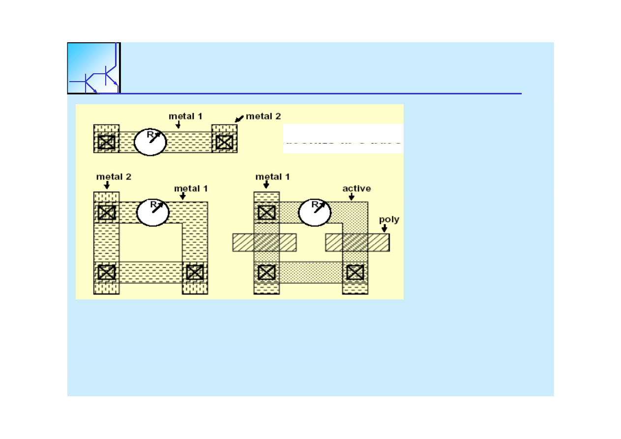
Layout disturbances
Layout disturbances
Layout disturbances
Layout disturbances
Green:
Green: desired shape
desired shape (as designed)
(as designed)
Red:
Red: actual shape
actual shape
Green:
Green: desired shape
desired shape (as designed)
(as designed)
Red:
Red: actual shape
actual shape
misalignment:
misalignment:
global disturbance
global disturbance
over/underetching:
over/underetching:
global disturbance
global disturbance
shape distortion:
shape distortion:
local disturbance
local disturbance
L
t di t b
l h
l b l d l
l
L
t di t b
l h
l b l d l
l
t S
t S
24 lutego 2010
Wojciech Kucewicz
21
Layout disturbances also have global and local
Layout disturbances also have global and local components. Some
components. Some
disturbances affect device
disturbances affect device performance, other don
performance, other don’’tt
Layout disturbances
Layout disturbances
Layout disturbances
Layout disturbances
Misalignment:
Misalignment:
W/L not affected
W/L not affected
Under/over etching:
Under/over etching:
change of W/L in a single
change of W/L in a single
device, but W/L(n) /W/L(p)
device, but W/L(n) /W/L(p) in
in
CMOS t
t ff t d
CMOS t
t ff t d
Shape distortion:
Shape distortion:
individual W/L change
individual W/L change in
in
every device
every device
S
di t b
ff t d i d i
it
f
S
di t b
ff t d i d i
it
f
a CMOS gate not affected
a CMOS gate not affected
24 lutego 2010
Wojciech Kucewicz
22
Some disturbances affect device and circuit performance,
Some disturbances affect device and circuit performance,
other don
other don’’tt
Deep submicron CMOS: new
Deep submicron CMOS: new
phenomena (examples)
phenomena (examples)
Deep submicron CMOS: new
Deep submicron CMOS: new
phenomena (examples)
phenomena (examples)
M l
l l
M l
l l
i i
f d i
i i
f d i
Molecular scale
Molecular scale variations of doping
variations of doping
Lithography:
Lithography: proximity effects
proximity effects
and corrections,
and corrections, phase shifting
phase shifting
masks
masks
It is expected that very deep submicron CMOS circuits will
It is expected that very deep submicron CMOS circuits will
24 lutego 2010
Wojciech Kucewicz
23
It is expected that very deep submicron CMOS circuits will
It is expected that very deep submicron CMOS circuits will
exhibit much higher sensitivity to process and layout
exhibit much higher sensitivity to process and layout disturbances.
disturbances.
Manufacturing imperfections vs.
Manufacturing imperfections vs.
faults: CMOS digital gates
faults: CMOS digital gates
Manufacturing imperfections vs.
Manufacturing imperfections vs.
faults: CMOS digital gates
faults: CMOS digital gates
Structural defects:
Structural defects:
• usually result in catastrophic faults
• usually result in catastrophic faults
usually result in catastrophic faults
usually result in catastrophic faults
• may affect performance
• may affect performance
Variations of device parameters:
Variations of device parameters:
• affect performance
• affect performance
• do not affect function
• do not affect function
Physical design:
Physical design:
Physical design:
Physical design:
• large number of small devices
• large number of small devices
• dense layout, dense wiring, large area
• dense layout, dense wiring, large area
y
g
g
y
g
g
--> sensitivity to structural defects
> sensitivity to structural defects
Structural defects are the most important source of faults
Structural defects are the most important source of faults in digital
in digital
24 lutego 2010
Wojciech Kucewicz
24
Structural defects are the most important source of faults
Structural defects are the most important source of faults in digital
in digital
CMOS circuits
CMOS circuits
Manufacturing imperfections vs.
Manufacturing imperfections vs.
faults: CMOS analog circuits
faults: CMOS analog circuits
Manufacturing imperfections vs.
Manufacturing imperfections vs.
faults: CMOS analog circuits
faults: CMOS analog circuits
Structural defects:
Structural defects:
• usually result in catastrophic faults
• usually result in catastrophic faults
f
ff
f
f
ff
f
• often affect performance
• often affect performance
Variations of device parameters:
Variations of device parameters:
• strongly affect performance
• strongly affect performance
strongly affect performance
strongly affect performance
• often affect function, resulting in
• often affect function, resulting in
catastrophic
catastrophic faults
faults
Ph si l d si :
Ph si l d si :
Physical design:
Physical design:
• small number of relatively large devices
• small number of relatively large devices
• low layout and wiring density, moderate
• low layout and wiring density, moderate
y
g
y,
y
g
y,
area
area
--> low sensitivity to structural defects
> low sensitivity to structural defects
24 lutego 2010
Wojciech Kucewicz
25
In analogue circuits variations of device parameters are
In analogue circuits variations of device parameters are usually more
usually more
important source of failures than structural
important source of failures than structural defects
defects
Fundamental
Fundamental model
model of a good IC design:
of a good IC design:
Fundamental
Fundamental model
model of a good IC design:
of a good IC design:
Gl b l
i ti
f d i
t
l
Gl b l
i ti
f d i
t
l
• Global variations of device parameters are large
• Global variations of device parameters are large
• Local variations of device parameters are small
• Local variations of device parameters are small
(1) Circuits are manufacturable if their performance is
(1) Circuits are manufacturable if their performance is insensitive to
insensitive to
absolute values of device parameters
absolute values of device parameters
(2) This is achieved if circuit performance depends on
(2) This is achieved if circuit performance depends on ratios of
ratios of
(2) This is achieved if circuit performance depends on
(2) This is achieved if circuit performance depends on ratios of
ratios of
device parameters ( device matching
device parameters ( device matching principle)
principle)
(3) Circuits based on device matching principle are
(3) Circuits based on device matching principle are manufacturable if
manufacturable if
24 lutego 2010
Wojciech Kucewicz
26
(3) Circuits based on device matching principle are
(3) Circuits based on device matching principle are manufacturable if
manufacturable if
device mismatch is not too big.
device mismatch is not too big.
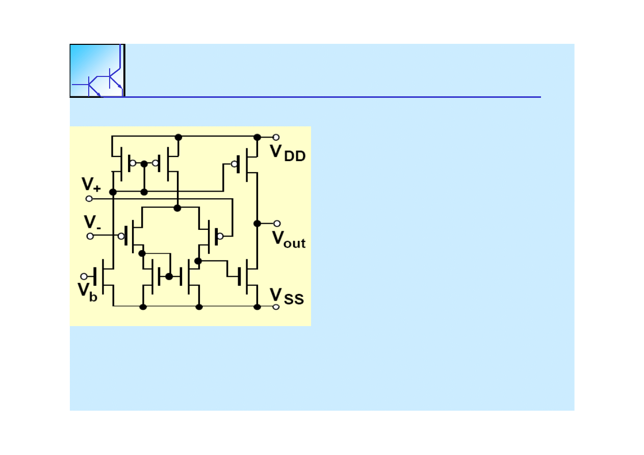
MOS transistor matching
MOS transistor matching
MOS transistor matching
MOS transistor matching
Kontaktowa
Kontaktowa
ó i
ó i
Potencjał
Potencjał
F
i
F
i
Ładunek
Ładunek
ó
ó
Ładunek
Ładunek
domieszek
domieszek
Koncentracja
Koncentracja
d i
ki
d i
ki
24 lutego 2010
Wojciech Kucewicz
27
różnica
różnica
potencjałów
potencjałów
me
me--pp
pp
Fermiego
Fermiego
równoważny
równoważny
stanów
stanów
powierzchniowych
powierzchniowych
domieszek
domieszek
zjonizowanych w
zjonizowanych w
półprzewodniku
półprzewodniku
domieszki w
domieszki w
zaimplantowanym
zaimplantowanym
kanale
kanale
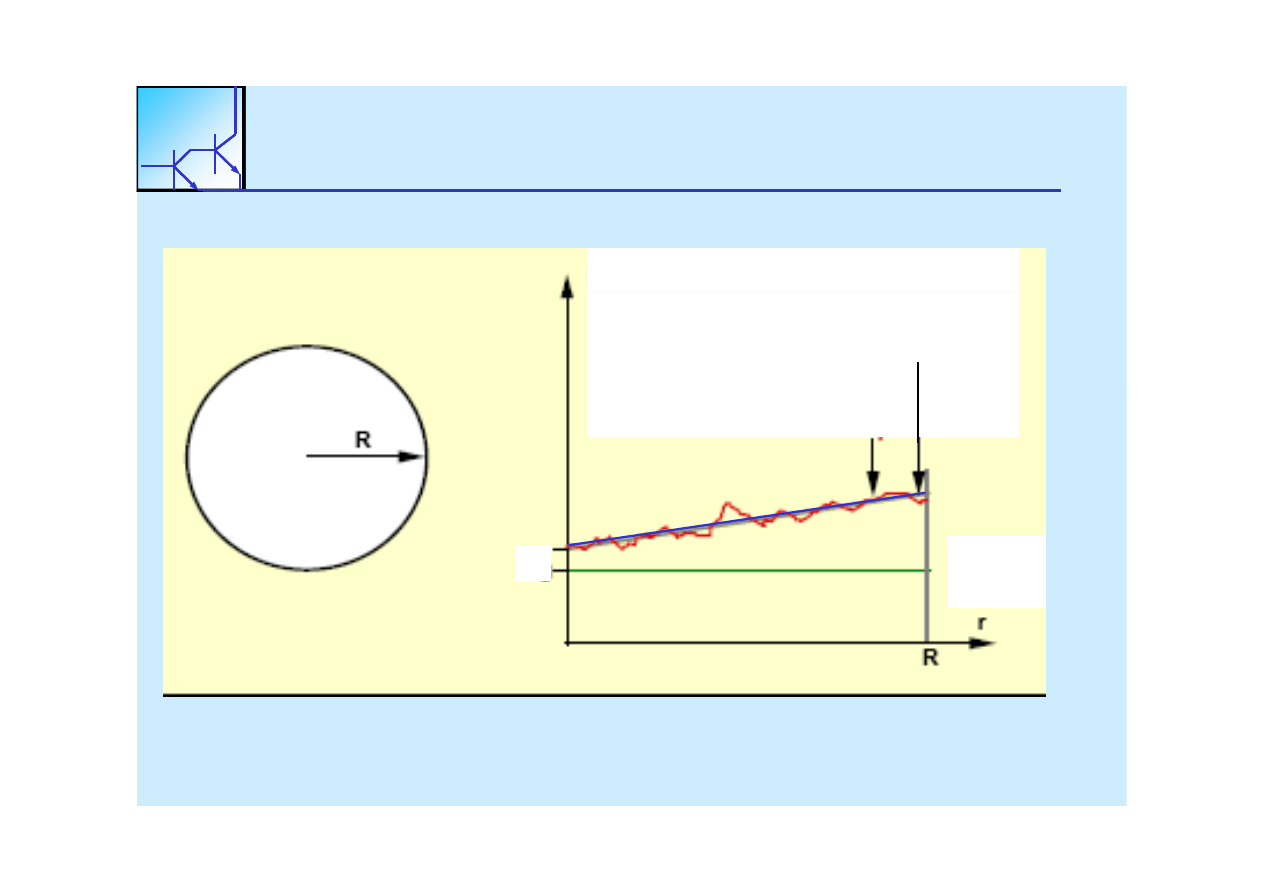
MOS transistor matching
MOS transistor matching
MOS transistor matching
MOS transistor matching
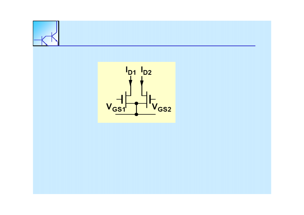
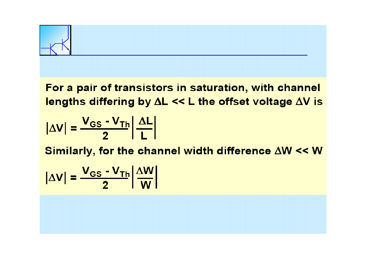
A good measure of matching: input offset voltage of a differential pair
A good measure of matching: input offset voltage of a differential pair
Δ
Δ
V = V
V = V
GS1
GS1
-- VV
GS2
GS2
-- a difference in gate voltages necessary to obtain equal drain currents
a difference in gate voltages necessary to obtain equal drain currents (assuming
(assuming
identical drain
identical drain--source voltages V
source voltages V
DS
DS
))
24 lutego 2010
Wojciech Kucewicz
28

MOS transistor matching
MOS transistor matching
MOS transistor matching
MOS transistor matching
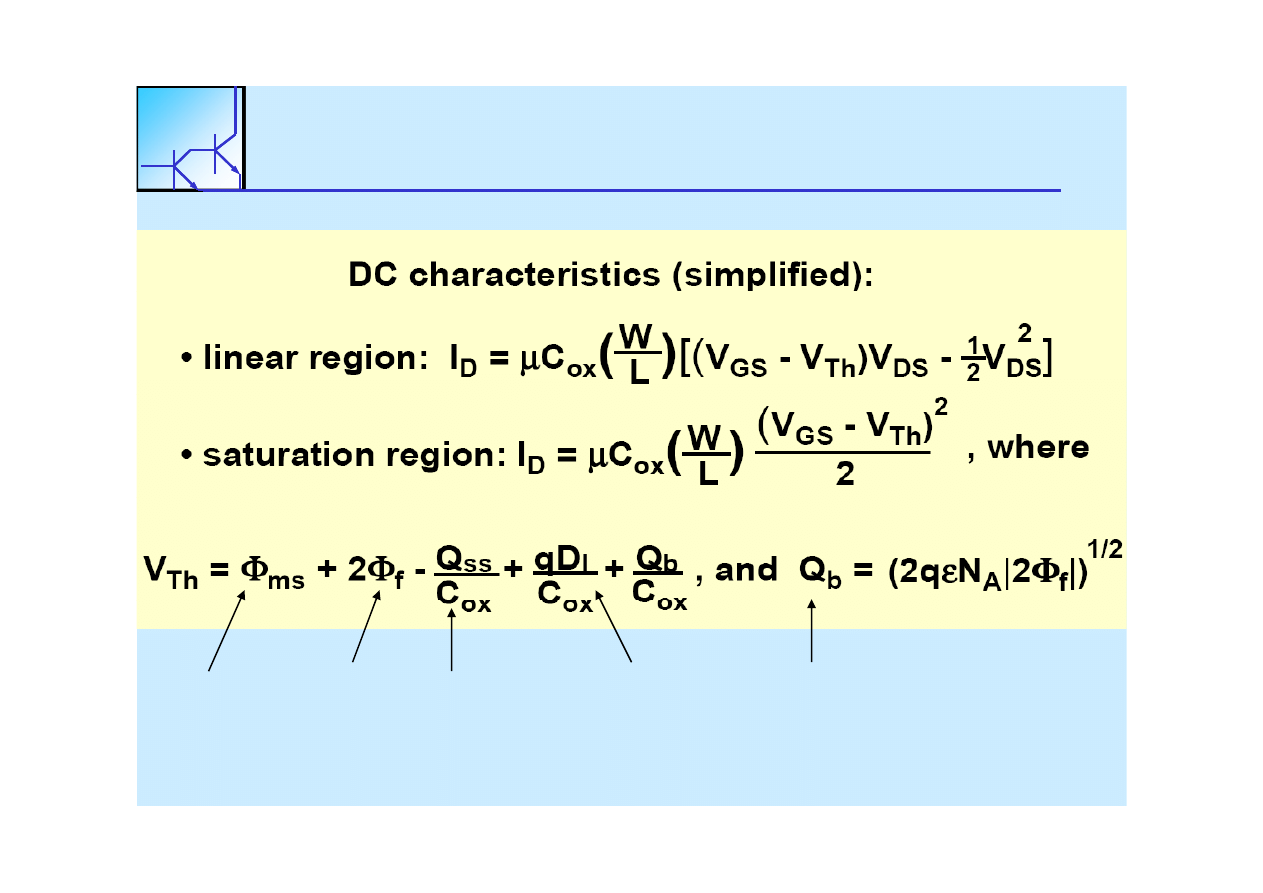
Variations affecting the drain current:
Variations affecting the drain current:
• Carrier mobility
• Carrier mobility μμ
Carrier mobility
Carrier mobility μμ
• Oxide capacitance C
• Oxide capacitance C
ox
ox
• Channel dimensions W, L
• Channel dimensions W, L
• Threshold voltage V
• Threshold voltage V
th
th
Variations affecting the threshold voltage:
Variations affecting the threshold voltage:
•
• Φ
Φ
ms
ms
, , Φ
Φ
ff
-- negligible effect (log functions of doping)
negligible effect (log functions of doping)
• Interface charge Q
• Interface charge Q
• Interface charge Q
• Interface charge Q
ss
ss
• Substrate doping N
• Substrate doping N
A
A
• Channel implant dose D
• Channel implant dose D
II
24 lutego 2010
Wojciech Kucewicz
29
pp
II
• Oxide capacitance C
• Oxide capacitance C
ox
ox
MOS transistor matching
MOS transistor matching
MOS transistor matching
MOS transistor matching
24 lutego 2010
Wojciech Kucewicz
30
MOS transistor matching
MOS transistor matching
MOS transistor matching
MOS transistor matching
24 lutego 2010
Wojciech Kucewicz
31
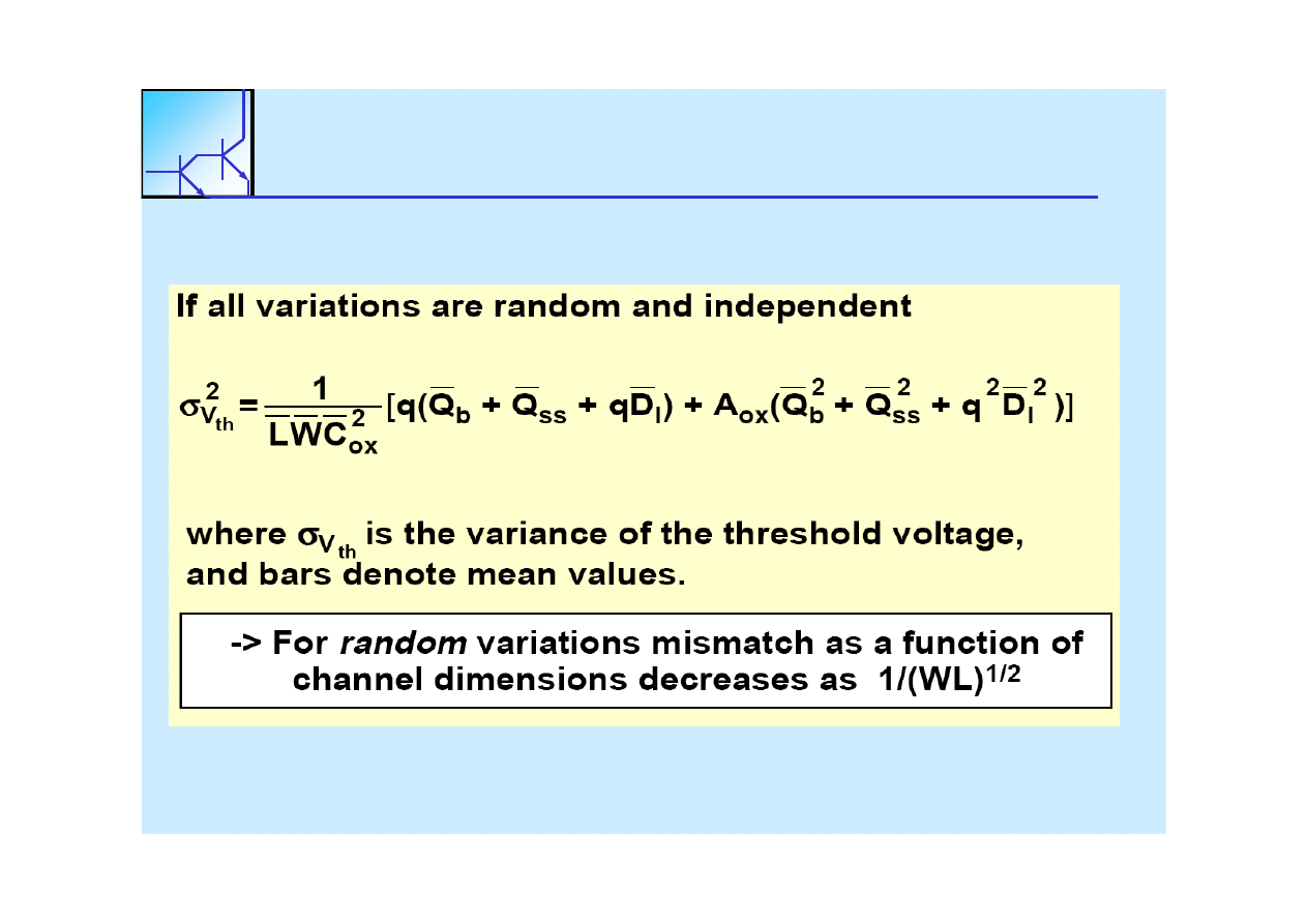
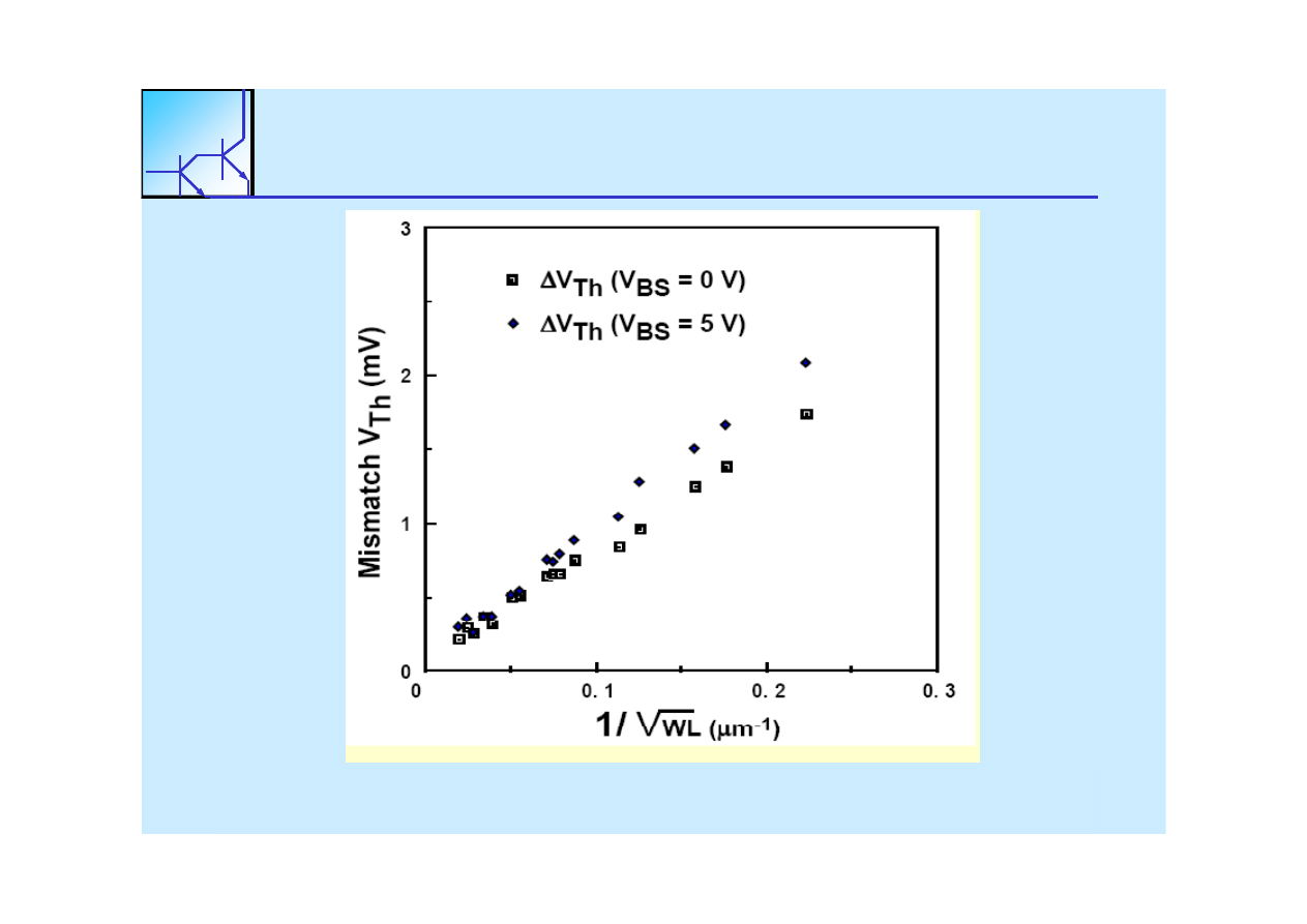
VV
Th
Th
mismatch as a function of device channel size
mismatch as a function of device channel size
MOS transistor matching
MOS transistor matching
MOS transistor matching
MOS transistor matching
24 lutego 2010
Wojciech Kucewicz
32
MOS transistor matching
MOS transistor matching
MOS transistor matching
MOS transistor matching
F d t hi
i i
di
si s t
b
s d!
F d t hi
i i
di
si s t
b
s d!
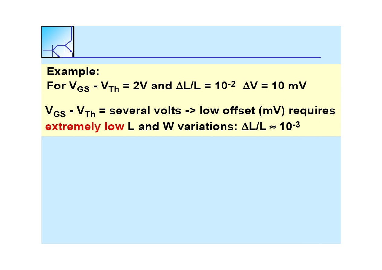
For good matching minimum dimensions cannot be used!
For good matching minimum dimensions cannot be used!
As a
As a result, there is a trade
result, there is a trade off between good matching and:
off between good matching and:
hi h f
f
hi h f
f
••high frequency performance,
high frequency performance,
••chip area.
chip area.
24 lutego 2010
Wojciech Kucewicz
33
MOS transistor matching
MOS transistor matching
MOS transistor matching
MOS transistor matching
24 lutego 2010
Wojciech Kucewicz
34
MOS transistor matching
MOS transistor matching
MOS transistor matching
MOS transistor matching
24 lutego 2010
Wojciech Kucewicz
35
Averaging of variations of V
Averaging of variations of V
Th
Th
MOS transistor matching
MOS transistor matching
MOS transistor matching
MOS transistor matching
Averaging of variations of V
Averaging of variations of V
Th
Th
C
t id l
t
ff ti l
d
i
t h
C
t id l
t
ff ti l
d
i
t h
lti
lti
24 lutego 2010
Wojciech Kucewicz
36
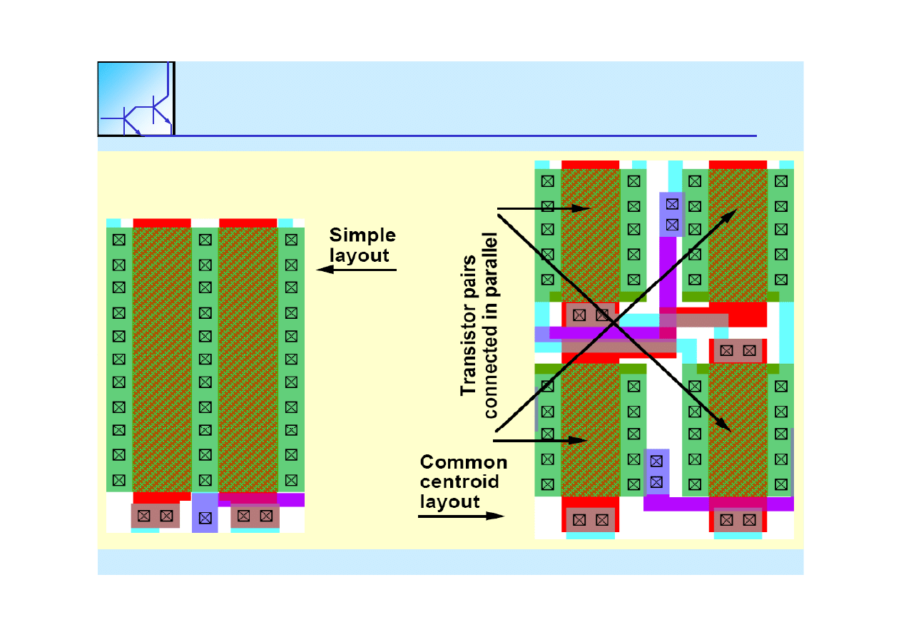
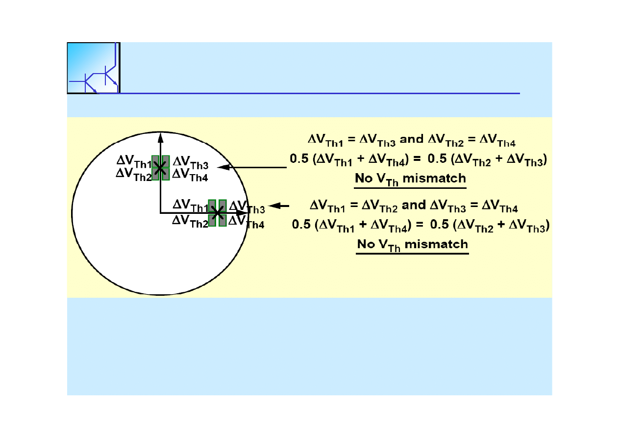
Common centroid layout very effectively reduces mismatch
Common centroid layout very effectively reduces mismatch resulting
resulting
from local deterministic variations
from local deterministic variations
MOS transistor matching
MOS transistor matching
MOS transistor matching
MOS transistor matching
For purely random variations
For purely random variations of
of
VV the probability density
the probability density
VV
Th
Th
the probability density
the probability density
functions of all four
functions of all four ΔΔVV
Th
Th
are
are the
the
same. Therefore, it doesn't
same. Therefore, it doesn't
matter whether transistors are
matter whether transistors are
matter whether transistors are
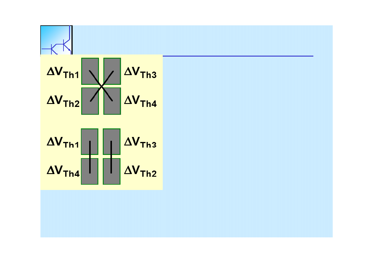
matter whether transistors are
cross
cross--connected or not.
connected or not.
Averaging of variations of V
Averaging of variations of V
Th
Th
C
t id l
t d
NOT d
i
t h
C
t id l
t d
NOT d
i
t h
lti f
lti f
24 lutego 2010
Wojciech Kucewicz
37
Common centroid layout does NOT reduce mismatch
Common centroid layout does NOT reduce mismatch resulting from
resulting from
local random variations
local random variations

Design for Manufacturability
Design for Manufacturability
Design for Manufacturability
Design for Manufacturability
Design for Manufacturability:
Design for Manufacturability:
••requires good understanding of the
requires good understanding of the sources of disturbances,
sources of disturbances,
••involves various design trade
involves various design trade--offs,
offs,
••is still considered
is still considered „„more art than
more art than Science
Science””
24 lutego 2010
Wojciech Kucewicz
38

Design for Manufacturability
Design for Manufacturability
Design for Manufacturability
Design for Manufacturability
Design for Manufacturability
Design for Manufacturability -- phase 1
phase 1
•• Selection and design of a circuit which is
Selection and design of a circuit which is inherently insensitive
inherently insensitive
gg
yy
to global variations of
to global variations of device parameters.
device parameters.
•• Design of a layout which does not violate design
Design of a layout which does not violate design rules and (if
rules and (if
)
i l
i t iti
l
)
i l
i t iti
l
t bt i
d d i
t bt i
d d i
necessary) uses simple intuitive rules
necessary) uses simple intuitive rules to obtain good device
to obtain good device
matching.
matching.
•• Verification of formal and functional correctness
Verification of formal and functional correctness of the design
of the design
Verification of formal and functional correctness
Verification of formal and functional correctness of the design
of the design
(DRC, circuit extraction, LVS and
(DRC, circuit extraction, LVS and post
post--layout circuit simulation
layout circuit simulation
with nominal values
with nominal values of device parameters).
of device parameters).
24 lutego 2010
Wojciech Kucewicz
39

Design for Manufacturability
Design for Manufacturability
Design for Manufacturability
Design for Manufacturability
Design for Manufacturability
Design for Manufacturability -- phase 2:
phase 2:
V ifi ti d ti i ti f th d i ith
V ifi ti d ti i ti f th d i ith
t t
t t
Verification and optimization of the design with
Verification and optimization of the design with respect to
respect to
secondary parasitic effects such as:
secondary parasitic effects such as:
••Thermal effects
Thermal effects
Thermal effects
Thermal effects
••Parasitic coupling, switching noise
Parasitic coupling, switching noise
••RF stability
RF stability
••RF stability
RF stability
••Signal propagation effects in long interconnects
Signal propagation effects in long interconnects
24 lutego 2010
Wojciech Kucewicz
40

Design for Manufacturability
Design for Manufacturability
Design for Manufacturability
Design for Manufacturability
Design for Manufacturability
Design for Manufacturability -- phase 3:
phase 3:
V ifi ti d i i i ti f
iti it t
V ifi ti d i i i ti f
iti it t
f t i
f t i
Verification and minimization of sensitivity to
Verification and minimization of sensitivity to manufacturing
manufacturing
imperfections:
imperfections:
••Worst case analysis (simulations for
Worst case analysis (simulations for process
process
Worst case analysis (simulations for
Worst case analysis (simulations for „„process
process
Corners
Corners””))
••Simple statistical Monte Carlo analysis
Simple statistical Monte Carlo analysis
••Simple statistical Monte Carlo analysis
Simple statistical Monte Carlo analysis
••Mismatch oriented statistical Monte Carlo
Mismatch oriented statistical Monte Carlo analysis
analysis
Netlist driven statistical process
Netlist driven statistical process device
device circuit
circuit Monte Carlo
Monte Carlo
••Netlist driven statistical process
Netlist driven statistical process--device
device--circuit
circuit Monte Carlo
Monte Carlo
simulation
simulation
24 lutego 2010
Wojciech Kucewicz
41

Conclusions
Conclusions
Conclusions
Conclusions
Methods of design for manufacturability are still not
Methods of design for manufacturability are still not part of the
part of the
standard engineering practices, in most
standard engineering practices, in most cases only simplest of them
cases only simplest of them
d
d
are used
are used
Understanding of the sources of variations and
Understanding of the sources of variations and mismatch and their
mismatch and their
effects on circuit performance
effects on circuit performance are necessary
are necessary blind
blind”” use of
use of
effects on circuit performance
effects on circuit performance are necessary,
are necessary, „„blind
blind use of
use of
methods and tools
methods and tools does not guarantee good results
does not guarantee good results
Special tools exist but are not always mature and are
Special tools exist but are not always mature and are seldom
seldom
p
y
p
y
available in standard commercial CAD toolsets
available in standard commercial CAD toolsets
24 lutego 2010
Wojciech Kucewicz
42
Wyszukiwarka
Podobne podstrony:
Brzoza biala Raport for herba i Nieznany (2)
European Society for Pediatric Nieznany
Anatomy Review For Neurosurgery Nieznany (2)
Nebulosity Tutorial for Canon U Nieznany
Neutrino Oscillations for Dummi Nieznany
European Society for Pediatric Nieznany (2)
4 week fat loss program for bus Nieznany
pro process for manufacturing
EdM wzmacniacze for stud id 150 Nieznany
DW Navigator only for web id 14 Nieznany
04 Wykonywanie podstawowych for Nieznany (2)
English for Medical S&D Practic Nieznany (3)
English for Medical S&D Practic Nieznany (2)
Damage Control Booklet CV for S Nieznany
Ancient Skeletal Evidence for L Nieznany (2)
English for Medical S&D Practic Nieznany
English for CE EE and water id Nieznany
więcej podobnych podstron