TA8029S
2002-02-27
1
TOSHIBA BIPOLAR LINEAR INTEGRATED CIRCUIT SILICON MONOLITHIC
TA8029S
FREQUENCY TO VOLTAGE CONVERTER
The TA8029S is a small 9
-
pin SIP IC incorporating an accurate
frequency / voltage converter and two voltage comparators.
It has a Schmitt input circuit and becomes active on the positive
edge of the input. Its F / V output is stable even when it is
supplied with a high
-
frequency input. Since the V
CC
pin connects
to a shunt regulator, stable frequency detection is assured
regardless of the battery voltage. In addition, its wide operating
temperature range allows it to be used for a wide variety of
applications.
FEATURES
l Schmitt input circuit incorporated
l Stable F / V output in response to high-frequency input
l Two comparators served by single power supplies are incorporated.
l Shunt regulator incorporated
l Operating temperature range : from −40~85°C
l Small plastic SIP
-
9 pin
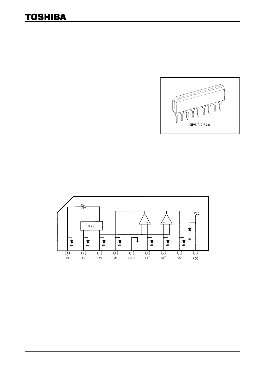
BLOCK DIAGRAM AND PIN LAYOUT
Weight: 0.92 g (typ.)
TA8029S
2002-02-27
2
PIN DESCRIPTION
PIN No.
SYMBOL
DESCRIPTION
1
IN
Frequency input pin. The IC becomes active on the leading edge of the input.
2
TC
One-shot pulse setting pin which connects to a capacitor.
3
F / V
F / V conversion output pin which connects to an charging capacitor and resistor. The signal
from this pin is also the input to the two built-in comparator.
4 O1
Comparator 1 output pin. This pin provides an NPN transistor open-collector output and has a
current capacity of up to 30mA.
5 GND
Grounded
6 I
1
+
Non-inverted PNP input pin for comparator 1.
7 I
2
+
Non-inverted PNP input pin for comparator 2.
8 O
2
Comparator 2 output pin. This pin provides an NPN transistor open-collector output and has a
current capacity of up to 30mA.
9 V
CC
Power supply pin which connects to a 6V Zener diode.
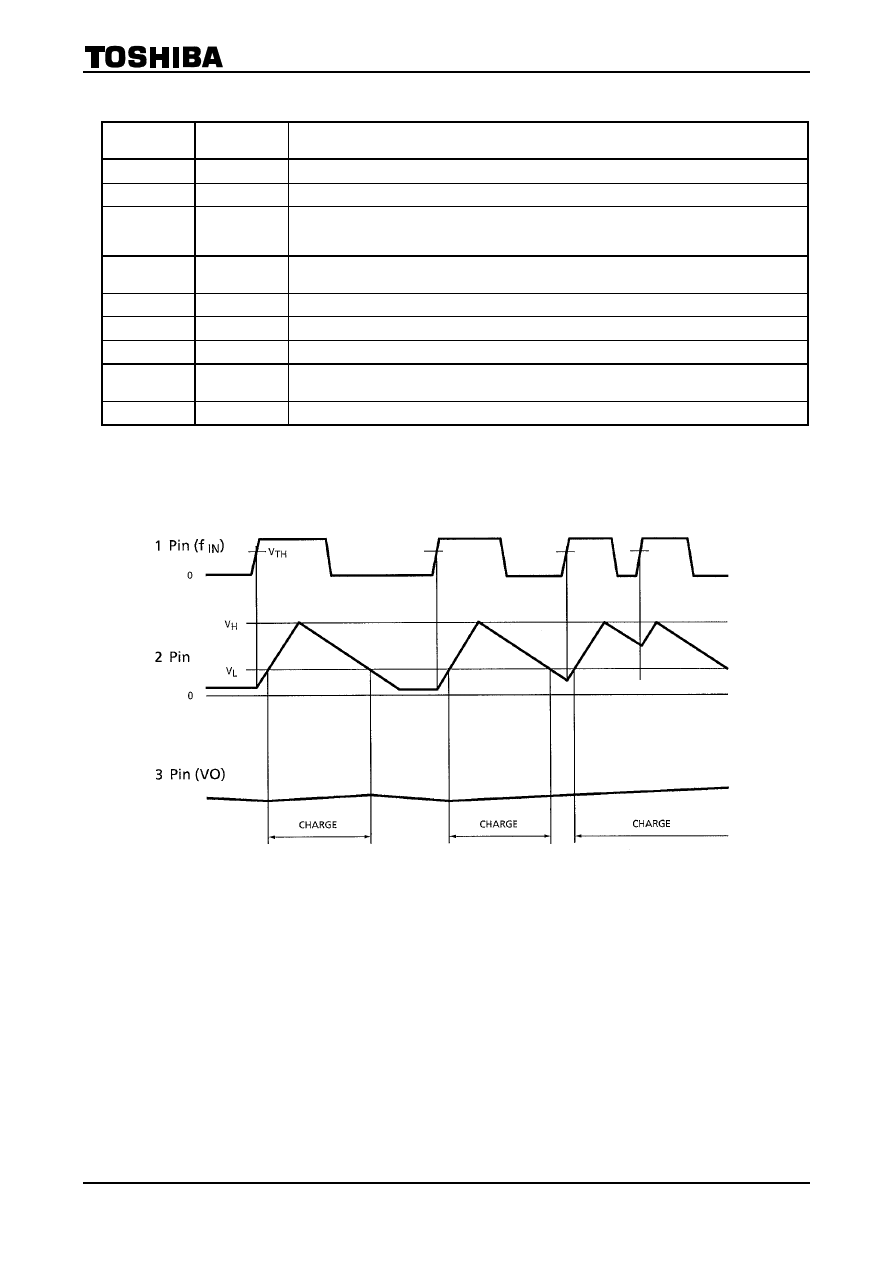
TIMING CHART
TA8029S
2002-02-27
3
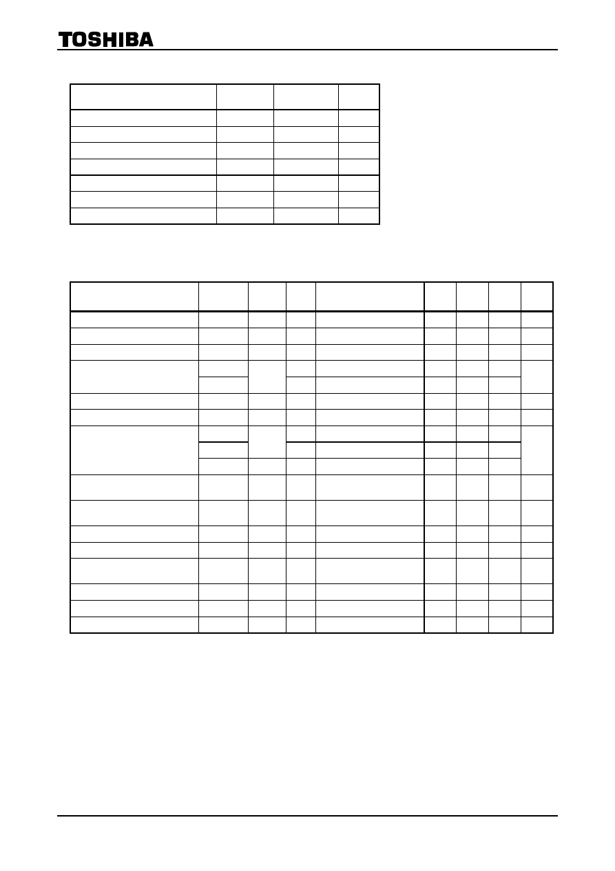
MAXIMUM RATINGS
(Ta = 25°C)
CHARACTERISTIC SYMBOL
RATING
UNIT
Supply Current
I
CC
30
mA
Input Voltage
V
IN
−0.3~30 V
Output Voltage
V
OUT
−0.3~30 V
Output Current
I
OUT
30
mA
Power Dissipation
P
D
350
(Note)
mW
Operating Temperature
T
opr
−40~85 °C
Storage Temperature
T
stg
−55~150 °C
Note: Ta≤85°C
ELECTRICAL CHARACTERISTICS
(Ta = 25°C, V
CC
= 5V)
CHARACTERISTIC SYMBOL
PIN
TEST
CIR-
CUIT
TEST CONDITION
MIN
TYP.
MAX
UNIT
Current Consumption
I
CC
V
CC
―
― 3.0 5 mA
Regulated Voltage
V
R
V
CC
―
I
CC
= 12mA
5.5
6.0
6.5
V
Input Current
I
IN
IN
―
V
IN
= 0~20V
−10
― 10 µA
V
IH
― 2.8
―
―
Input Voltage
V
IL
IN
―
―
― 0.8
V
Input Rise Rate
V
LH
IN
― 0.5
―
― V
/
ms
Input Fall Rate
V
HL
IN
― 0.1
―
― V
/
ms
I
OL
―
V
TC
= 2.5V
― 43 ―
I
OH
TC
―
V
TC
= 2.5V
―
−73
―
Output Current
I
OH
F
/
V
―
−250
−350
−500
µA
F / V Conversion Coefficient
K
F / V
―
C
T
= 0.01µF, R
T
= 27kΩ
f = 100Hz
(Note 1)
― 7.8 ―
―
Linearity
―
C
T
= 0.01µF, R
T
= 27kΩ
(Note
2)
― ±3.0 ― %
Input Offset Voltage
V
IO
I
1
+
/ I
2
+
―
― 2 10 mV
Input Current
I
IN
I
1
+
/ I
2
+
―
―
−0.2
−1 µA
Common-mode Input Voltage
V
CM
I
1
+
/ I
2
+
― 0
―
V
CC
−1.5
V
Voltage Gain
A
V
―
― 100 ― dB
Output Voltage
V
OL
O
1
/ O
2
―
I
OL
= 10mA
―
― 0.5 V
Output Leakage Current
I
LEAK
O
1
/ O
2
―
V
O
= 16V
―
― 5 µA
Notes:
1. Calculated from V
O
= K·V
CC
·C
T
·R
T
·f
2. Straight line deviation at f = 50Hz and f = 150Hz relative to that at f = 100Hz
TA8029S
2002-02-27
4
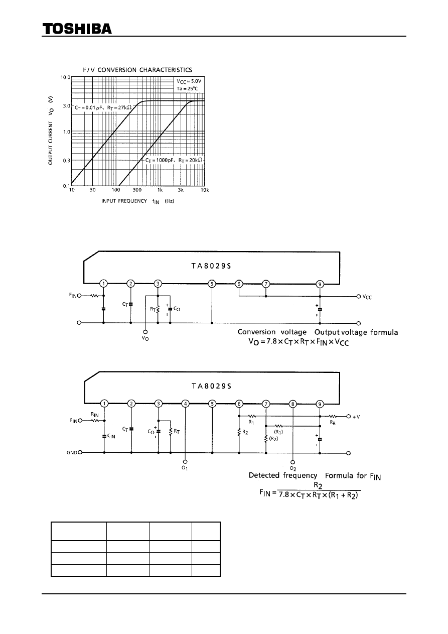
STANDARD CHARACTERISTICS
EXAMPLE OF APPLICATION CIRCUIT
1. FREQUENCY−VOLTAGE CONVERSION CIRCUIT
2. FREQUENCY DETECTION CIRCUIT
RECOMMENDED CONDITION
PART NAME
MIN
MAX
UNIT
C
T
1000
pF
R
T
20
kΩ
f
IN
5
kHz
TA8029S
2002-02-27
5
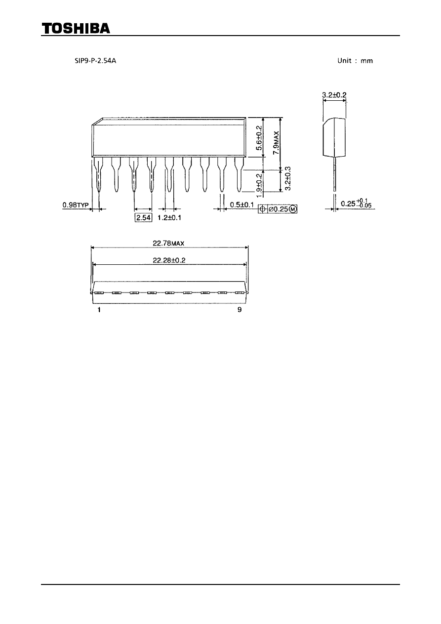
PACKAGE DIMENSIONS
Weight: 0.92g (Typ.)
TA8029S
2002-02-27
6
· TOSHIBA is continually working to improve the quality and reliability of its products. Nevertheless, semiconductor
devices in general can malfunction or fail due to their inherent electrical sensitivity and vulnerability to physical
stress. It is the responsibility of the buyer, when utilizing TOSHIBA products, to comply with the standards of
safety in making a safe design for the entire system, and to avoid situations in which a malfunction or failure of
such TOSHIBA products could cause loss of human life, bodily injury or damage to property.
In developing your designs, please ensure that TOSHIBA products are used within specified operating ranges as
set forth in the most recent TOSHIBA products specifications. Also, please keep in mind the precautions and
conditions set forth in the “Handling Guide for Semiconductor Devices,” or “TOSHIBA Semiconductor Reliability
Handbook” etc..
· The information contained herein is presented only as a guide for the applications of our products. No
responsibility is assumed by TOSHIBA CORPORATION for any infringements of intellectual property or other
rights of the third parties which may result from its use. No license is granted by implication or otherwise under
any intellectual property or other rights of TOSHIBA CORPORATION or others.
· The information contained herein is subject to change without notice.
000707EAA_S
RESTRICTIONS ON PRODUCT USE
Wyszukiwarka
Podobne podstrony:
en 2sk1489 20040726 datasheet
PENDRIVE s100 datasheet en 15
3RV20111HA10 datasheet en
0a esp8266ex datasheet en
6ES73211BH500AA0 datasheet en
EcoSolar Datasheet Phoenix Inverter 180VA 1200VA EN
3RA61201DP32 datasheet en
6ES73401AH020AE0 datasheet en
6AV66470AC113AX0 datasheet en
Datasheet BlueSolar charge controller MPPT 75 50 & MPPT 100 50 EN
datasheet c400 en
6ES73146CH040AB0 datasheet en
6ES72151AG400XB0 datasheet en (1)
cooper csa datasheet easicheck 2 testing system emergency luminaires en
6ES73146CG030AB0 datasheet en
EN Game Capture HD Datasheet
KACO Datasheet 16 18TR3 EN 120106
więcej podobnych podstron