L2: 6.111 Spring 2006
1
Introductory Digital Systems Laboratory
L2: Combinational Logic Design
L2: Combinational Logic Design
(Construction and Boolean Algebra)
(Construction and Boolean Algebra)
Acknowledgements:
Materials in this lecture are courtesy of the following sources and are used with permission.
Prof. Randy Katz (Unified Microelectronics Corporation Distinguished Professor in Electrical
Engineering and Computer Science at the University of California, Berkeley) and Prof. Gaetano
Borriello (University of Washington Department of Computer Science & Engineering) from Chapter 2
of R. Katz, G. Borriello. Contemporary Logic Design. 2nd ed. Pentice-Hall/Pearson Education, 2005.
J. Rabaey, A. Chandrakasan, B. Nikolic. Digital Integrated Circuits: A Design Perspective.
Prentice Hall/Pearson, 2003.
L2: 6.111 Spring 2006
2
Introductory Digital Systems Laboratory
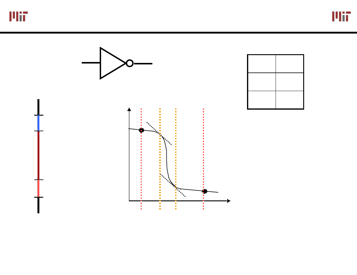
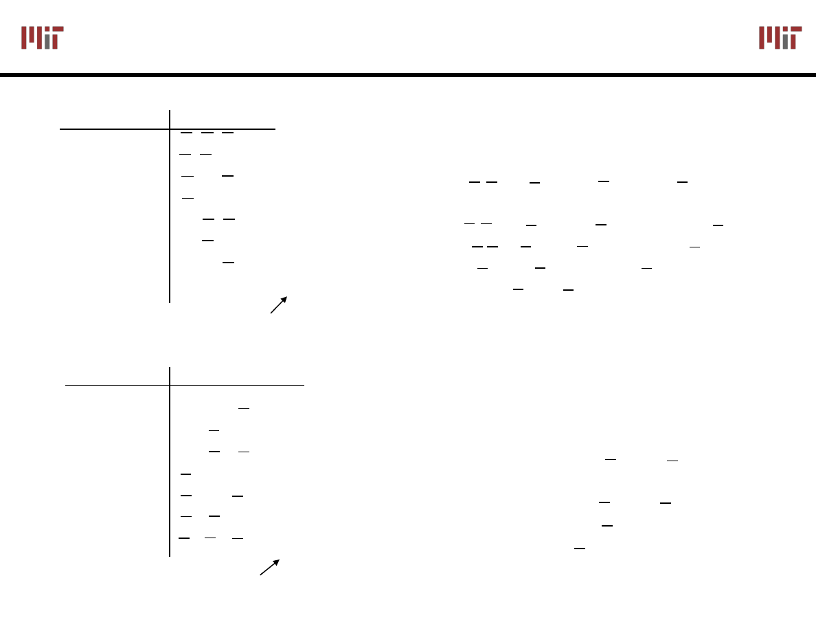
Review: Noise Margin
Review: Noise Margin
IN
OUT
IN
OUT
0
1
1
0
V(x)
V(y)
VOH
VOL
V
IH
V
IL
Slope = -1
Slope = -1
V
OL
VOH
"1"
"0"
V
OH
V
IH
V
IL
V
OL
Undefined
Region
Large noise margins
protect against various noise sources
NM
L
= V
IL
-V
OL
NM
H
= V
OH
-V
IH
Truth Table
L2: 6.111 Spring 2006
3
Introductory Digital Systems Laboratory
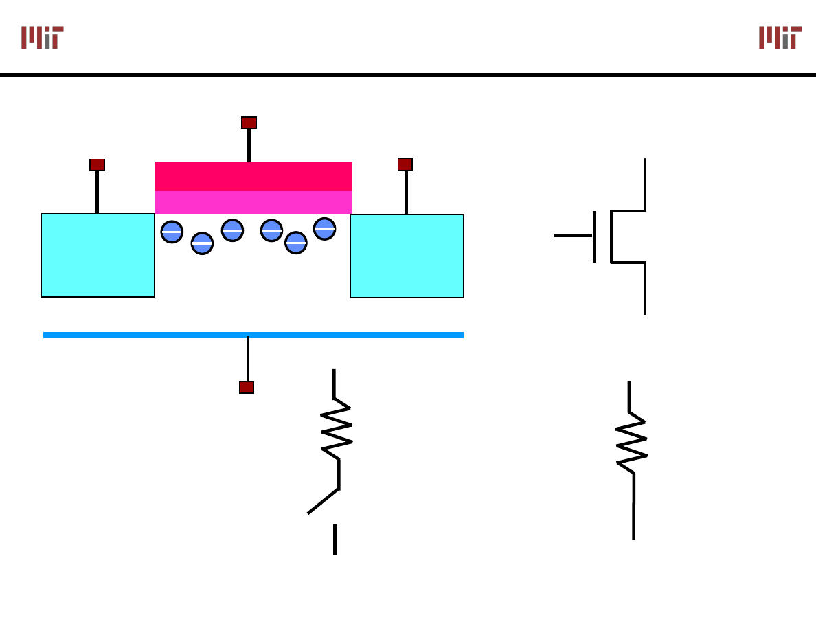
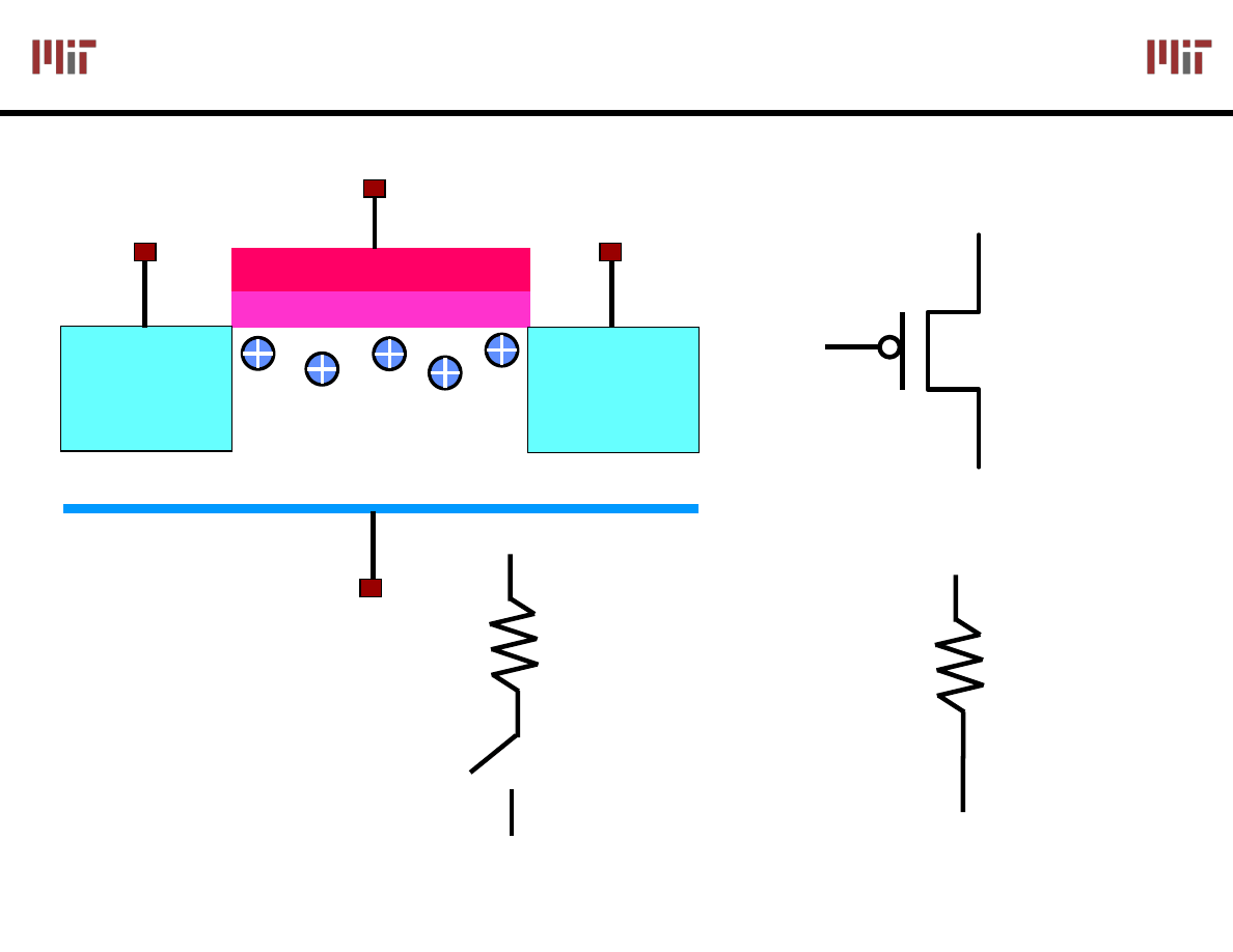
MOS Technology: The NMOS Switch
MOS Technology: The NMOS Switch
D
G
S
gate
N+
P-substrate
N+
drain
source
R
NMOS
Switch
Model
V
T
= 0.5V
V
GS
< V
T
OFF
R
NMOS
V
GS
> V
T
ON
V
s
NMOS ON when Switch Input is High
L2: 6.111 Spring 2006
4
Introductory Digital Systems Laboratory
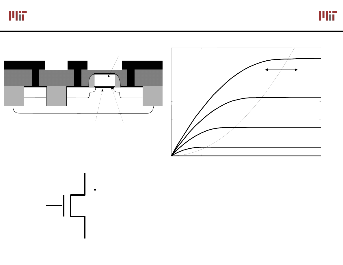
NMOS Device Characteristics
NMOS Device Characteristics
0
0.5
1
1.5
2
2.5
0
VGS= 1.0 V
V
DS
(V)
D
G
V
T
= 0.5V
I
D
¾ MOS is a very non-linear.
+
¾ Switch-resistor model
V
GS
sufficient for first order analysis.
-
1
2
3
4
5
6
D
(A)
VGS= 2.5 V
VGS= 2.0 V
VGS= 1.5 V
Resistive
Saturation
x 10
-4
I
S
polysilicon gate
body
source
drain
gate
p
p+
n+
n+
n+
inversion layer�
gate oxide
n
channel
L2: 6.111 Spring 2006
5
Introductory Digital Systems Laboratory
PMOS: The Complementary Switch
PMOS: The Complementary Switch
S
G
D
gate
P+
N-substrate
P+
drain
source
R
PMOS
Switch
Model
V
T
= -0.5V
V
GS
> V
T
OFF
R
PMOS
V
GS
< V
T
ON
PMOS ON when Switch Input is Low
V
DD
L2: 6.111 Spring 2006
6
Introductory Digital Systems Laboratory
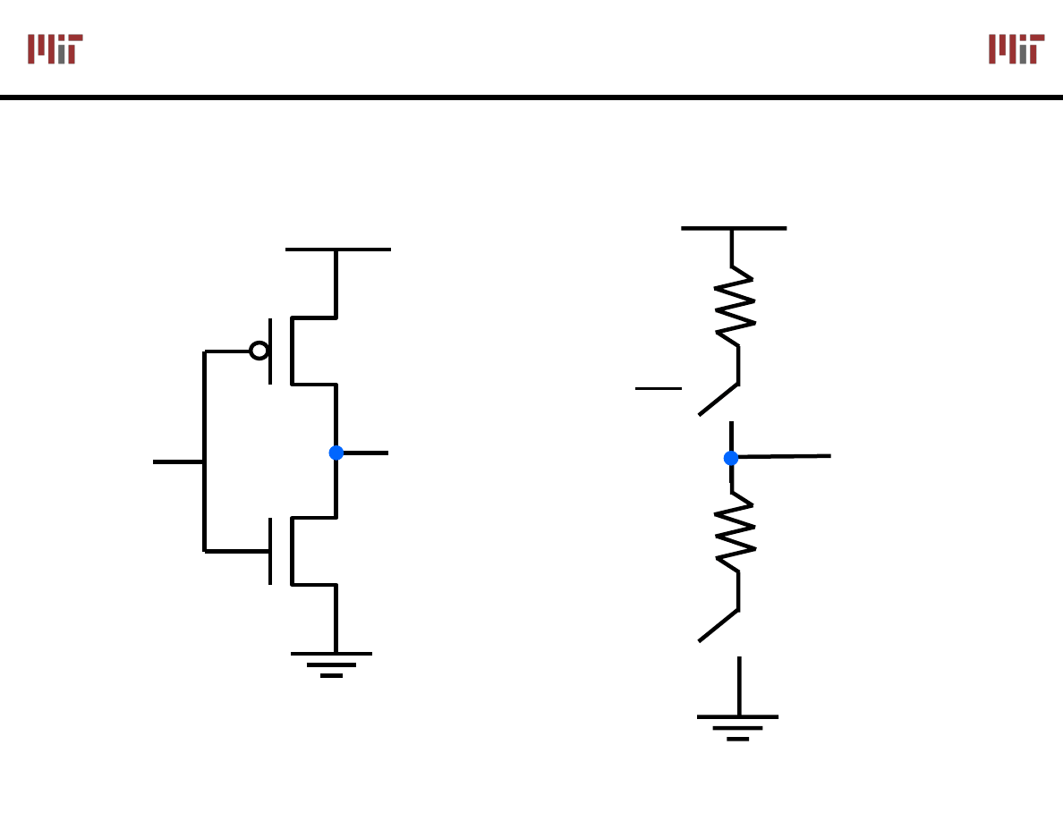
The CMOS Inverter
The CMOS Inverter
IN
OUT
V
DD
V
DD
OUT
R
PMOS
R
NMOS
IN
IN
Switch Model
S
G
G
D
D
S
Rail-to-rail Swing in CMOS
L2: 6.111 Spring 2006
7
Introductory Digital Systems Laboratory
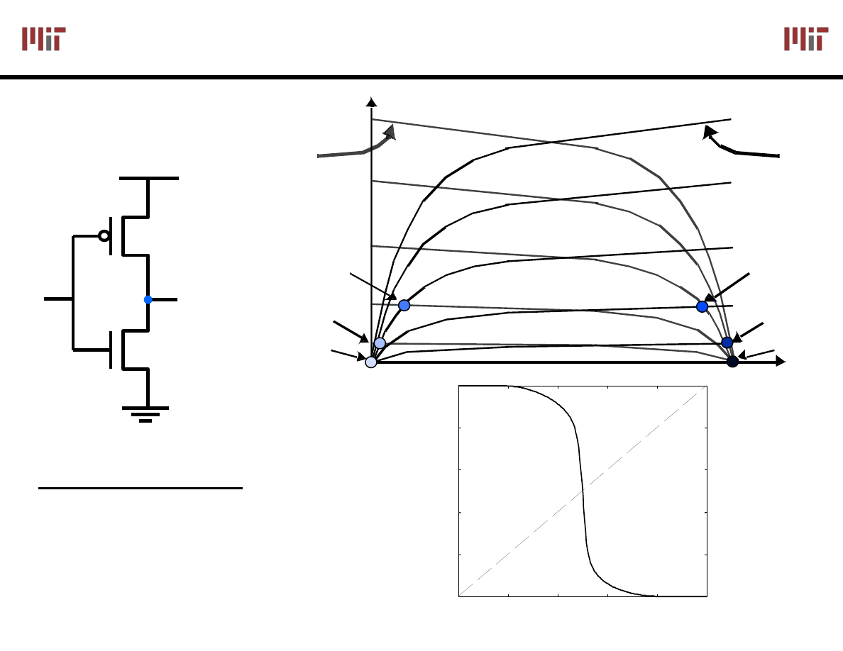
Inverter VTC: Load Line Analysis
Inverter VTC: Load Line Analysis
IN
OUT
V
DD
S
G
D
D
S
G
I
D n
V
out
V
in
= 2.5
V
in
= 2
V
in
= 1.5
V
in
= 0
V
in
= 0.5
V
in
= 1
NMOS
V
in
= 0
V
in
= 0.5
V
in
= 1
V
in
= 1.5
V
in
= 2
V
in
= 2.5
V
in
= 1
V
in
= 1.5
PMOS
0
0.5
1
1.5
2
2.5
0
0.5
1
1.5
2
2.5
V
in
(V)
V
out
(V
)
CMOS gates have:
Rail-to-rail swing (0V to V
DD
)
Large noise margins
“zero” static power dissipation
L2: 6.111 Spring 2006
8
Introductory Digital Systems Laboratory
Possible Function of Two Inputs
Possible Function of Two Inputs
X
Y
F
X
Y
16 possible functions (F
0
–F
15
)
0
0 0
0
0
0
0
0
0
0
1
1
1
1
1
1
1
1
0
1 0
0
0
0
1
1
1
1
0
0
0
0
1
1
1
1
1
0 0
0
1
1
0
0
1
1
0
0
1
1
0
0
1
1
1
1 0
1
0
1
0
1
0
1
0
1
0
1
0
1
0
1
X
Y
X
NOR
Y
NOT
(X
OR
Y)
X
NAND
Y
NOT
(X
AND
Y)
1
0
NOT
X
X
AND
Y
X
OR
Y
NOT
Y
X
XOR
Y
X = Y
There are 16 possible functions of 2 input variables:
In general, there are 2
(2^n)
functions of n inputs
L2: 6.111 Spring 2006
9
Introductory Digital Systems Laboratory
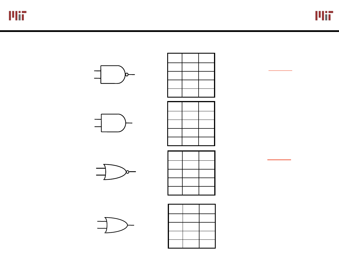
Common Logic Gates
Common Logic Gates
X
Y
Z
Z
X
Y
X
Y
Z
0
0
1
1
0
1
1
1
0
1
1
0
NAND
Gate
Symbol
Truth-Table
Expression
X
Y
Z
0
0
1
1
0
1
1
0
0
0
1
0
NOR
Z = X • Y
Z = X + Y
Z
X
Y
X
Y
Z
0
0
1
1
0
0
1
1
0
1
1
1
OR
Z = X + Y
X
Y
Z
X
Y
Z
0
0
1
1
0
0
1
0
0
0
1
1
AND
Z = X • Y
L2: 6.111 Spring 2006
10
Introductory Digital Systems Laboratory
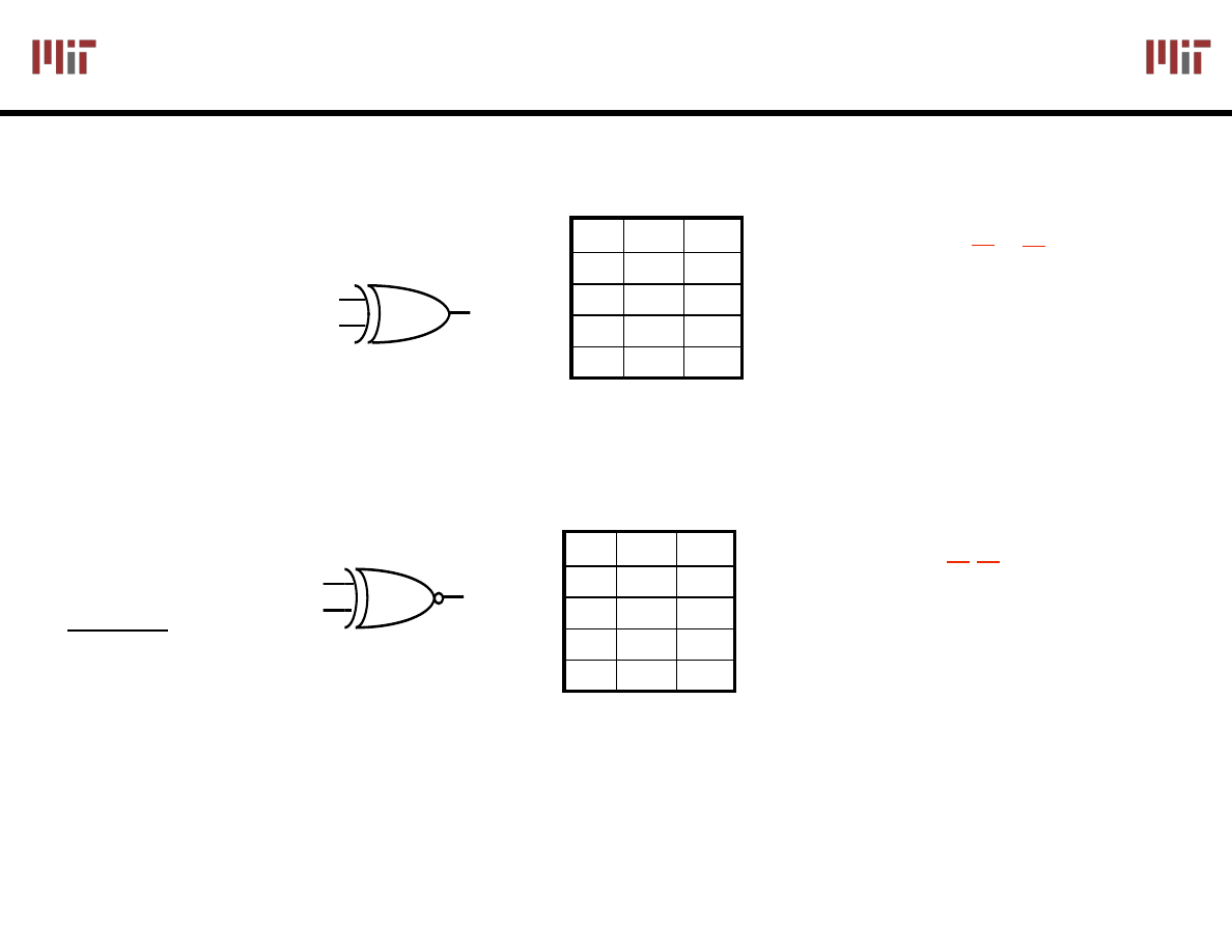
Exclusive (N)OR Gate
Exclusive (N)OR Gate
X
Y
Z
Z
X
Y
X
Y
Z
0
0
1
1
0
0
1
1
0
1
1
0
X
Y
Z
0
0
1
1
0
1
1
0
0
0
1
1
XOR
(X ⊕ Y)
XNOR
(X ⊕ Y)
Widely used in arithmetic structures such as adders and multipliers
Z = X Y + X Y
X or Y but not both
("inequality", "difference")
Z = X Y + X Y
X and Y the same
("equality")
L2: 6.111 Spring 2006
11
Introductory Digital Systems Laboratory
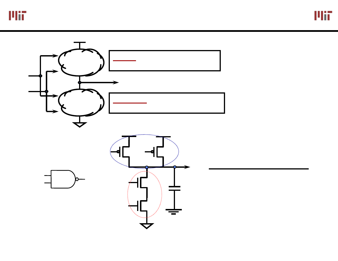
Generic CMOS Recipe
Generic CMOS Recipe
V
dd
A
1
F(A
1
,…,A
n
)
pullup
: make this connection
when we want F(A
1
,…,A
n
) = 1
pulldown
: make this connection
when we want F(A
1
,…,A
n
) = 0
A
n
...
...
...
A
B
A B PDN PUN O
0 0 0ff
0n
1
0 1 0ff
0n
1
1 0 0ff
0n
1
1 1
0n
0ff 0
B
A
C
L
PUN
PDN
How do you build a 2-input NOR Gate?
A
B
Note:
CMOS gates
result in inverting
functions!
(easier to build NAND
vs. AND)
O

L2: 6.111 Spring 2006
12
Introductory Digital Systems Laboratory
Theorems of Boolean Algebra (I)
Theorems of Boolean Algebra (I)
Elementary
1. X + 0 = X
1D. X • 1 = X
2. X + 1 = 1
2D. X • 0 = 0
3. X + X = X
3D. X • X = X
4. (X) = X
5. X + X = 1
5D. X • X = 0
Commutativity:
6. X + Y = Y + X
6D. X • Y = Y • X
Associativity:
7. (X + Y) + Z = X + (Y + Z)
7D. (X • Y) • Z = X • (Y • Z)
Distributivity:
8. X • (Y + Z) = (X • Y) + (X • Z)
8D. X + (Y • Z) = (X + Y) • (X + Z)
Uniting:
9. X • Y + X • Y = X
9D. (X + Y) • (X + Y) = X
Absorption:
10. X + X • Y = X
10D. X • (X + Y) = X
11. (X + Y) • Y = X • Y
11D. (X • Y) + Y = X + Y

L2: 6.111 Spring 2006
13
Introductory Digital Systems Laboratory
Theorems of Boolean Algebra (II)
Theorems of Boolean Algebra (II)
Factoring:
12. (X
•
Y) + (X • Z) =
12D. (X + Y) • (X + Z) =
X • (Y + Z)
X + (Y • Z)
Consensus:
13. (X • Y) + (Y • Z) + (X • Z) =
13D. (X + Y) • (Y + Z) • (X + Z) =
X • Y + X • Z
(X + Y) • (X + Z)
De Morgan's:
14.
(X + Y + ...) = X • Y • ...
14D.
(X • Y • ...) = X + Y + ...
Generalized De Morgan's:
15. f(X1,X2,...,Xn,0,1,+,•) = f(X1,X2,...,Xn,1,0,•,+)
Duality
Dual of a Boolean expression is derived by replacing • by +, + by •, 0
by 1, and 1 by 0, and leaving variables unchanged
f (X1,X2,...,Xn,0,1,+,•)
⇔ f(X1,X2,...,Xn,1,0,•,+)
L2: 6.111 Spring 2006
14
Introductory Digital Systems Laboratory
Simple Example: One Bit Adder
Simple Example: One Bit Adder
1-bit binary adder
inputs: A, B, Carry-in
outputs: Sum, Carry-out
A
B
Cin
Cout
S
A B
Cin S Cout
0
0
0
0
0
1
0
1
0
0
1
1
1
0
0
1
0
1
1
1
0
1
1
1
0
1
1
0
1
0
0
1
0
0
0
1
0
1
1
1
Sum-of-Products Canonical Form
S = A B Cin + A B Cin + A B Cin + A B Cin
Cout = A B Cin + A B Cin + A B Cin + A B Cin
Product term (or minterm)
ANDed product of literals – input combination for which output
is true
Each variable appears exactly once, in true or inverted form (but
not both)

L2: 6.111 Spring 2006
15
Introductory Digital Systems Laboratory
Simplify Boolean Expressions
Simplify Boolean Expressions
Cout
= A B Cin + A B Cin + A B Cin + A B Cin
= A B Cin +
A B Cin
+ A B Cin +
A B Cin
+ A B Cin +
A B Cin
= (A + A) B Cin + A (B + B) Cin + A B (Cin + Cin)
= B Cin + A Cin + A B
= (B + A) Cin + A B
S = A B Cin + A B Cin + A B Cin + A B Cin
=( A B + A B )Cin + (A B + A B) Cin
=(A ⊕ B) Cin + (A ⊕ B) Cin
= A ⊕ B ⊕ Cin
L2: 6.111 Spring 2006
16
Introductory Digital Systems Laboratory
Sum
Sum
-
-
of
of
-
-
Products & Product
Products & Product
-
-
of
of
-
-
Sum
Sum
short-hand notation form in terms of 3 variables
A
B
C
minterms
0
0
0
A B C
m0
0
0
1
A B C
m1
0
1
0
A B C
m2
0
1
1
A B C
m3
1
0
0
A B C
m4
1
0
1
A B C
m5
1
1
0
A B C
m6
1
1
1
A B C
m7
F in canonical form:
F(A, B, C) = Σm(1,3,5,6,7)
= m1 + m3 + m5 + m6 + m7
canonical form ≠ minimal form
F(A, B, C) = A B C + A B C + AB C + ABC + ABC
= (A B + A B + AB + AB)C + ABC
= ((A + A)(B + B))C + ABC
= C + ABC = ABC + C = AB + C
Product term
(or minterm): ANDed product of literals – input combination for which output is true
F =
+ A B C+ A B C + A B C + ABC
A B C
A
B
C
maxterms
0
0
0
A + B + C
M0
0
0
1
A + B + C M1
0
1
0
A + B + C
M2
0
1
1
A + B + C M3
1
0
0
A + B + C
M4
1
0
1
A + B+ C
M5
1
1
0
A + B +C
M6
1
1
1
A +B + C
M7
short-hand notation for maxterms of 3 variables
F in canonical form:
F(A, B, C) = ΠM(0,2,4)
= M0 • M2 • M4
= (A + B + C) (A + B + C) (A + B + C)
canonical form ≠ minimal form
F(A, B, C) = (A + B + C) (A + B + C) (A + B + C)
= (A + B + C) (A + B + C)
(A + B + C) (A + B + C)
= (A + C) (B + C)
Sum term
(or maxterm) - ORed sum of literals – input combination for which output is false
L2: 6.111 Spring 2006
17
Introductory Digital Systems Laboratory
Mapping Between Forms
Mapping Between Forms
1.
Minterm to Maxterm conversion:
rewrite minterm shorthand using maxterm shorthand
replace minterm indices with the indices not already used
E.g., F(A,B,C) =
Σm(3,4,5,6,7) = ΠM(0,1,2)
2.
Maxterm to Minterm conversion:
rewrite maxterm shorthand using minterm shorthand
replace maxterm indices with the indices not already used
E.g., F(A,B,C) =
ΠM(0,1,2) = Σm(3,4,5,6,7)
3.
Minterm expansion of F to Minterm expansion of F':
in minterm shorthand form, list the indices not already used in F
E.g., F(A,B,C) =
Σm(3,4,5,6,7) F'(A,B,C) = Σm(0,1,2)
=
ΠM(0,1,2) = ΠM(3,4,5,6,7)
4.
Minterm expansion of F to Maxterm expansion of F':
rewrite in Maxterm form, using the same indices as F
E.g., F(A,B,C) =
Σm(3,4,5,6,7) F'(A,B,C) = ΠM(3,4,5,6,7)
=
ΠM(0,1,2) = Σm(0,1,2)
L2: 6.111 Spring 2006
18
Introductory Digital Systems Laboratory
The Uniting Theorem
The Uniting Theorem
A
B
F
0
0
1
0
1
0
1
0
1
1
1
0
B has the same value in both on-set rows
– B remains
A has a different value in the two rows
– A is eliminated
F = A B +AB = (A +A)B = B
Key tool to simplification: A (B + B) = A
Essence of simplification of two-level logic
Find two element subsets of the ON-set where only one variable
changes its value – this single varying variable can be
eliminated and a single product term used to represent both
elements
L2: 6.111 Spring 2006
19
Introductory Digital Systems Laboratory
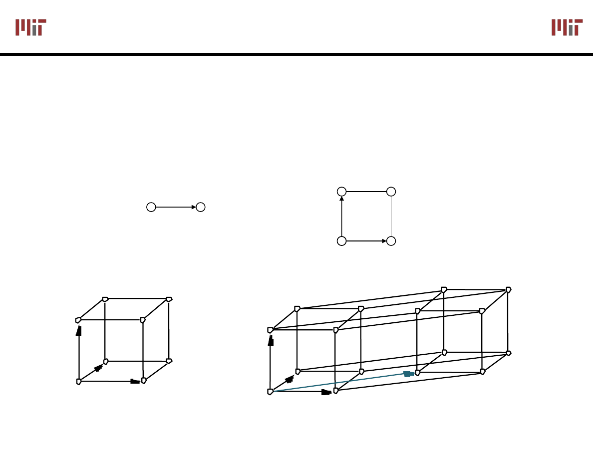
Boolean Cubes
Boolean Cubes
1-cube
X
0
1
Just another way to represent truth table
Visual technique for identifying when the uniting theorem
can be applied
n input variables = n-dimensional "cube"
2-cube
X
Y
11
00
01
10
WXYZ
0111
0011
0010
0000
0001
0110
1010
0101
0100
1000
1011
1001
1110
1111
1101
1100
Y
Z
W
X
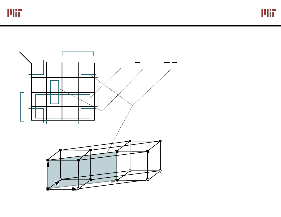
3-cube
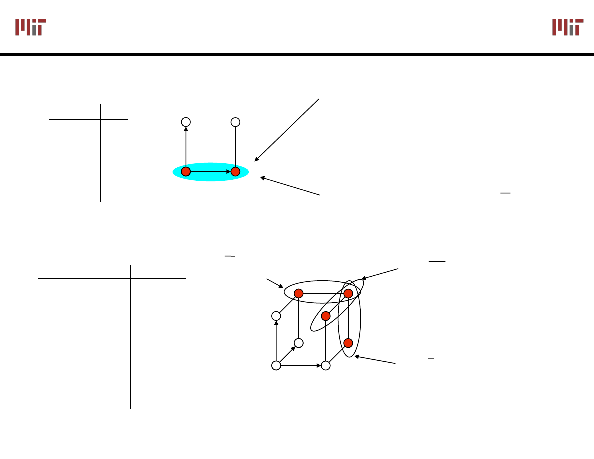
XYZ
X
011
010
000
001
111
110
100
101
Y
Z
4-cube
XY
L2: 6.111 Spring 2006
20
Introductory Digital Systems Laboratory
A
B
F
0
0
1
0
1
0
1
0
1
1
1
0
ON-set = solid nodes
OFF-set = empty nodes
Circled group of the on-set is called the
adjacency
plane. Each adjacency plane
corresponds to a product term.
A varies within face, B does not
this face represents the literal B
Mapping Truth Tables onto Boolean Cubes
Mapping Truth Tables onto Boolean Cubes
Uniting theorem
A
B
11
00
01
10
F
A B
Cin
Cout
0
0
0
0
0
0
1
0
0
1
0
0
0
1
1
1
1
0
0
0
1
0
1
1
1
1
0
1
1
1
1
1
Cout = BCin+AB+ACin
A(B+B)Cin
The on-set is completely covered by the combination (OR) of the subcubes of
lower dimensionality - note that “111” is covered three times
A
B C
000
111
101
(A+A)BCin
AB(Cin+Cin)
Three variable example: Binary full-adder carry-out logic
L2: 6.111 Spring 2006
21
Introductory Digital Systems Laboratory
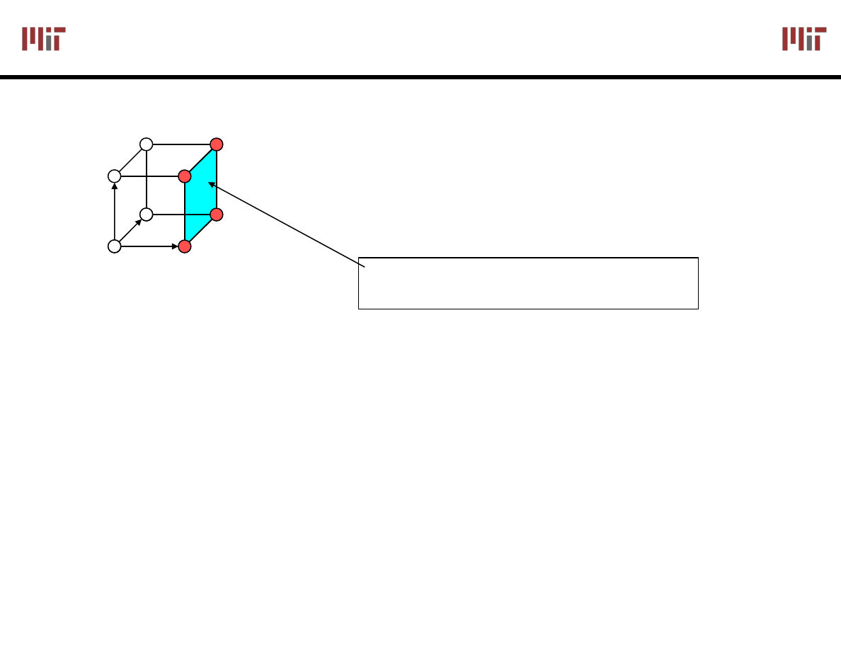
Higher Dimension Cubes
Higher Dimension Cubes
F(A,B,C) = Σm(4,5,6,7)
on-set forms a square
i.e., a cube of dimension 2 (2-D adjacency plane)
represents an expression in one variable
i.e., 3 dimensions – 2 dimensions
A is asserted (true) and unchanged
B and C vary
This subcube represents the literal A
A
B C
000
111
101
100
001
010
011
110
In a 3-cube (three variables):
0-cube, i.e., a single node, yields a term in 3 literals
1-cube, i.e., a line of two nodes, yields a term in 2 literals
2-cube, i.e., a plane of four nodes, yields a term in 1 literal
3-cube, i.e., a cube of eight nodes, yields a constant term "1"
In general,
m-subcube within an n-cube (m < n) yields a term with n – m
literals
L2: 6.111 Spring 2006
22
Introductory Digital Systems Laboratory
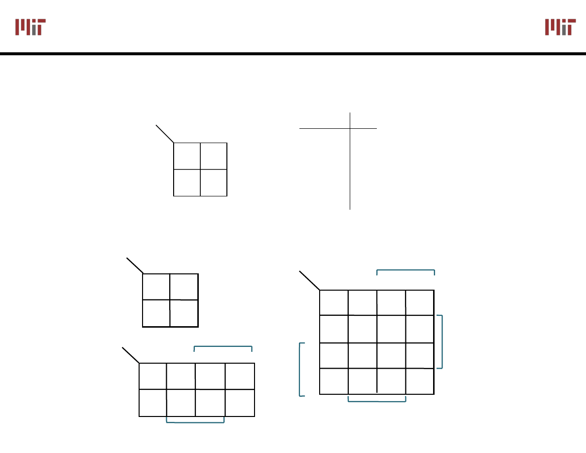
Karnaugh
Karnaugh
Maps
Maps
A
B
F
0
0
1
0
1
0
1
0
1
1
1
0
Alternative to truth-tables to help visualize adjacencies
Guide to applying the uniting theorem - On-set elements with only one
variable changing value are adjacent unlike in a linear truth-table
0
2
1
3
0
1
A
B
0
1
1
0
0
1
Numbering scheme based on Gray–code
e.g., 00, 01, 11, 10 (only a single bit changes in code for adjacent map cells)
A
B
0 1
0
1
0
1
2
3
0
1
2
3
6
7
4
5
AB
C
0
1
3
2
4
5
7
6
12
13
15
14
8
9
11
10
A
B
AB
CD
A
00 01 11 10
0
1
00 01 11 10
00
01
11
10
C
B
D
2-variable
K-map
3-variable
K-map
4-variable
K-map
L2: 6.111 Spring 2006
23
Introductory Digital Systems Laboratory
K
K
-
-
Map Examples
Map Examples
Cout =
F(A,B,C) =
A B
A
B
Cin
00 01 11 10
0
1
0
0
0
1
1
1
0
1
AB
C
A
00 01 11 10
0
1
0
0
0
0
1
1
1
1
B
F(A,B,C) =
Σm(0,4,5,7)
F =
00
C
AB
01 11 10
1
0
0
1
1
1
0
0
A
B
0
1
00
C
AB
01 11 10
0
1
1
0
0
0
1
1
A
B
0
1
F' simply replace 1's with 0's and vice versa
F'(A,B,C) =
Σm(1,2,3,6)
F' =
L2: 6.111 Spring 2006
24
Introductory Digital Systems Laboratory
Four Variable
Four Variable
Karnaugh
Karnaugh
Map
Map
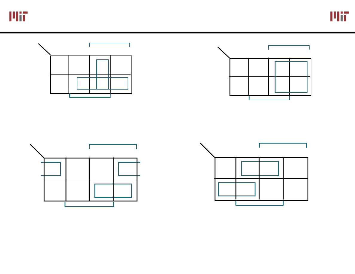
F(A,B,C,D) =
Σm(0,2,3,5,6,7,8,10,11,14,15)
F = C + A B D + B D
K-map Corner Adjacency
Illustrated in the 4-Cube
Find the smallest number
of the largest possible
subcubes that cover the
ON-set
AB
00 01 11 10
1 0 0 1
0 1 0 0
1 1 1 1
1 1 1 1
00
01
11
10
C
CD
A
D
B
0011
D
0010
0000
0111
0110
0001
C
A
B
0100
1000
1100
1101
1111
1110
1001
1011
1010
0101
L2: 6.111 Spring 2006
25
Introductory Digital Systems Laboratory
K
K
-
-
Map Example: Don
Map Example: Don
’
’
t Cares
t Cares
F(A,B,C,D) =
Σm(1,3,5,7,9) + Σd(6,12,13)
F = A D + B C D w/o don't cares
F = C D + A D w/ don't cares
Don't Cares can be treated as 1's or 0's if it is advantageous to do so
Don't Cares can be treated as 1's or 0's if it is advantageous to do so
By treating this DC as a "1", a 2-cube
can be formed rather than one 0-cube
AB
00 01 11 10
0 0 X 0
1 1 X 1
1 1 0 0
0 X 0 0
00
01
11
10
C
CD
A
D
B
AB
00 01 11 10
0 0 X 0
1 1 X 1
1 1 0 0
0 X 0 0
00
01
11
10
C
CD
A
D
B
In PoS form: F = D (A + C)
Equivalent answer as above,
but fewer literals
L2: 6.111 Spring 2006
26
Introductory Digital Systems Laboratory
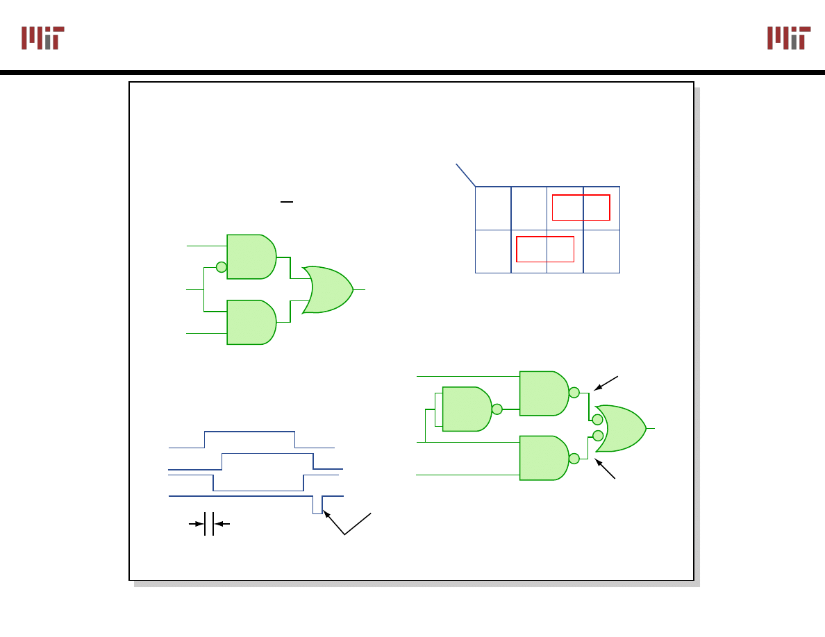
Hazards
Hazards
Figure by MIT OpenCourseWare.
A
C
B
A = B = 1
C
1
2
F
Gate delay
Glitch
F
Static hazards: Consider this function:
Implemented with MSI gates:
'00
'00
'00
'00
A
C
B
F
2
1
C
AB
00 01 11 10
0 0
0
0
0
1
1
1
1
1
F = A * C + B * C
L2: 6.111 Spring 2006
27
Introductory Digital Systems Laboratory
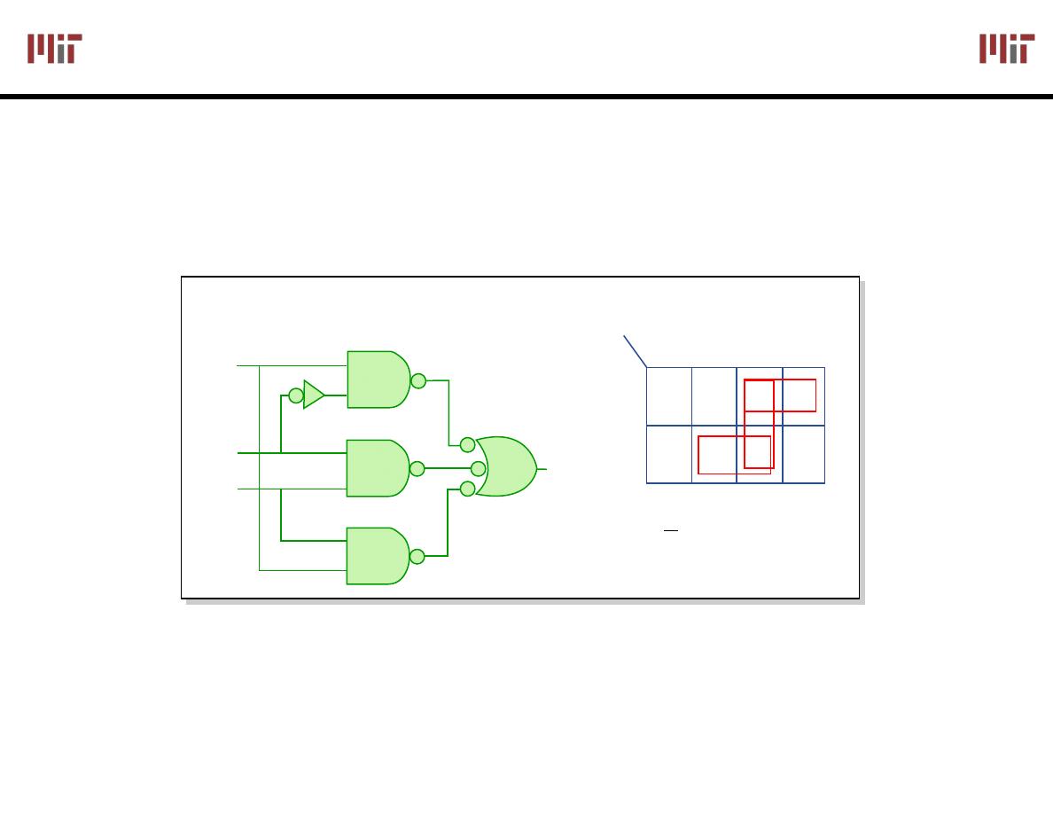
Fixing Hazards
Fixing Hazards
In general, it is difficult to avoid hazards – need a robust
design methodology to deal with hazards.
The glitch is the result of timing differences
in parallel data paths. It is associated with the
function jumping between groupings or product
terms on the K-map. To fix it, cover it up with
another grouping or product term!
Figure by MIT OpenCourseWare.
C
AB
00 01 11 10
0 0 0
0
0
1 1
1
1
1
A
C
B
F
F = A * C + B * C + A * B
Document Outline
- L2: Combinational Logic Design (Construction and Boolean Algebra)
- Review: Noise Margin
- MOS Technology: The NMOS Switch
- NMOS Device Characteristics
- PMOS: The Complementary Switch
- The CMOS Inverter
- Inverter VTC: Load Line Analysis
- Possible Function of Two Inputs
- Common Logic Gates
- Exclusive (N)OR Gate
- Generic CMOS Recipe
- Theorems of Boolean Algebra (I)
- Theorems of Boolean Algebra (II)
- Simple Example: One Bit Adder
- Simplify Boolean Expressions
- Sum-of-Products & Product-of-Sum
- Mapping Between Forms
- The Uniting Theorem
- Boolean Cubes
- Higher Dimension Cubes
- Karnaugh Maps
- K-Map Examples
- Four Variable Karnaugh Map
- K-Map Example: Don’t Cares
- Hazards
- Fixing Hazards
Wyszukiwarka
Podobne podstrony:
L2 2 id 257126 Nieznany
Fuzzy Logic III id 182424 Nieznany
mk2 l2 id 303715 Nieznany
Fuzzy Logic II id 182423 Nieznany
BST L2 id 93597 Nieznany
Instrukcja L2 id 216866 Nieznany
L2 2 id 257126 Nieznany
Abolicja podatkowa id 50334 Nieznany (2)
4 LIDER MENEDZER id 37733 Nieznany (2)
katechezy MB id 233498 Nieznany
metro sciaga id 296943 Nieznany
perf id 354744 Nieznany
interbase id 92028 Nieznany
Mbaku id 289860 Nieznany
Probiotyki antybiotyki id 66316 Nieznany
miedziowanie cz 2 id 113259 Nieznany
LTC1729 id 273494 Nieznany
D11B7AOver0400 id 130434 Nieznany
więcej podobnych podstron