REV. 0
Information furnished by Analog Devices is believed to be accurate and
reliable. However, no responsibility is assumed by Analog Devices for its
use, nor for any infringements of patents or other rights of third parties
which may result from its use. No license is granted by implication or
otherwise under any patent or patent rights of Analog Devices.
a
AD8036/AD8037
and large-signal bandwidths and ultralow distortion. The
AD8036 achieves –66 dBc at 20 MHz, and 240 MHz small-
signal and 195 MHz large-signal bandwidths. The AD8036 and
AD8037’s recover from 2
×
clamp overdrive within 1.5 ns.
These characteristics position the AD8036/AD8037 ideally for
driving as well as buffering flash and high resolution ADCs.
In addition to traditional output clamp amplifier applications,
the input clamp architecture supports the clamp levels as addi-
tional inputs to the amplifier. As such, in addition to static dc
clamp levels, signals with speeds up to 240 MHz can be applied
to the clamp pins. The clamp values can also be set to any
value within the output voltage range provided that V
H
is greater
that V
L
. Due to these clamp characteristics, the AD8036 and
AD8037 can be used in nontraditional applications such as a
full-wave rectifier, a pulse generator, or an amplitude modula-
tor. These novel applications are only examples of some of the
diverse applications which can be designed with input clamps.
The AD8036 is offered in chips, industrial (–40
°
C to +85
°
C)
and military (–55
°
C to +125
°
C) package temperature ranges
and the AD8037 in industrial. Industrial versions are available
in plastic DIP and SOIC; MIL versions are packaged in cerdip.
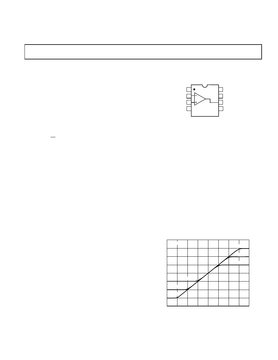
–4 –3 –2 –1 0 1 2 3 4
4
3
2
1
0
–1
–2
–3
–4
INPUT VOLTAGE – Volts
OUTPUT VOLTAGE – Volts
V
L
= –3V
V
L
= –2V
V
L
= –1V
V
H
= 1V
V
H
= 2V
V
H
= 3V
AD8036
Figure 1. Clamp DC Accuracy vs. Input Voltage
FEATURES
Superb Clamping Characteristics
3 mV Clamp Error
1.5 ns Overdrive Recovery
Minimized Nonlinear Clamping Region
240 MHz Clamp Input Bandwidth
±
3.9 V Clamp Input Range
Wide Bandwidth
AD8036
AD8037
Small Signal
240 MHz
270 MHz
Large Signal (4 V p-p) 195 MHz
190 MHz
Good DC Characteristics
2 mV Offset
10
µ
V/
°
C Drift
Ultralow Distortion, Low Noise
–72 dBc typ @ 20 MHz
4.5 nV/
√
Hz Input Voltage Noise
High Speed
Slew Rate 1500 V/
µ
s
Settling 10 ns to 0.1%, 16 ns to 0.01%
±
3 V to
±
5 V Supply Operation
APPLICATIONS
ADC Buffer
IF/RF Signal Processing
High Quality Imaging
Broadcast Video Systems
Video Amplifier
Full Wave Rectifier
FUNCTIONAL BLOCK DIAGRAM
8-Pin Plastic Mini-DIP (N), Cerdip (Q),
and SO (R) Packages
Low Distortion, Wide Bandwidth
Voltage Feedback Clamp Amps
PRODUCT DESCRIPTION
The AD8036 and AD8037 are wide bandwidth, low distortion
clamping amplifiers. The AD8036 is unity gain stable. The
AD8037 is stable at a gain of two or greater. These devices al-
low the designer to specify a high (V
CH
) and low (V
CL
) output
clamp voltage. The output signal will clamp at these specified
levels. Utilizing a unique patent pending CLAMPIN™ input
clamp architecture, the AD8036 and AD8037 offer a 10
×
im-
provement in clamp performance compared to traditional out-
put clamping devices. In particular, clamp error is typically
3 mV or less and distortion in the clamp region is minimized.
This product can be used as a classical op amp or a clamp am-
plifier where a high and low output voltage are specified.
The AD8036 and AD8037, which utilize a voltage feedback ar-
chitecture, meet the requirements of many applications which
previously depended on current feedback amplifiers. The
AD8036 and AD8037 exhibit an exceptionally fast and accurate
pulse response (16 ns to 0.01%), extremely wide small-signal
CLAMPIN is a trademark of Analog Devices, Inc.
1
2
3
4
NC
–INPUT
+INPUT
–V
S
V
H
+V
S
OUTPUT
V
L
8
7
6
5
AD8036/37
TOP VIEW
NC = NO CONNECT
© Analog Devices, Inc., 1994
One Technology Way, P.O. Box 9106, Norwood. MA 02062-9106, U.S.A.
Tel: 617/329-4700
Fax: 617/326-8703

AD8036/AD8037–SPECIFICATIONS
ELECTRICAL CHARACTERISTICS
REV. 0
–2–
(
±
V
S
=
±
5 V; R
LOAD
= 100
Ω
; A
V
= +1 (AD8036); A
V
= +2 (AD8037), V
H
, V
L
open, unless
otherwise noted)
AD8036A
AD8037A
Parameter
Conditions
Min
Typ
Max
Min
Typ
Max
Units
DYNAMIC PERFORMANCE
Bandwidth (–3 dB)
Small Signal
V
OUT
≤
0.4 V p-p
150
240
200
270
MHz
Large Signal
1
8036, V
OUT
= 2.5 V p-p; 8037, V
OUT
= 3.5 V p-p 160
195
160
190
MHz
Bandwidth for 0.1 dB Flatness
V
OUT
≤
0.4 V p-p
8036, R
F
= 140
Ω
; 8037, R
F
= 274
Ω
130
130
MHz
Slew Rate, Average +/–
V
OUT
= 4 V Step, 10–90%
900
1200
1100 1500
V/
µ
s
Rise/Fall Time
V
OUT
= 0.5 V Step, 10–90%
1.4
1.2
ns
V
OUT
= 4 V Step, 10–90%
2.6
2.2
ns
Settling Time
To 0.1%
V
OUT
= 2 V Step
10
10
ns
To 0.01%
V
OUT
= 2 V Step
16
16
ns
HARMONIC/NOISE PERFORMANCE
2nd Harmonic Distortion
2 V p-p; 20 MHz, R
L
= 100
Ω
–59
–52
–52
–45
dBc
R
L
= 500
Ω
–66
–59
–72
–65
dBc
3rd Harmonic Distortion
2 V p-p; 20 MHz, R
L
= 100
Ω
–68
–61
–70
–63
dBc
R
L
= 500
Ω
–72
–65
–80
–73
dBc
3rd Order Intercept
25 MHz
+46
+41
dBm
Noise Figure
R
S
= 50
Ω
18
14
dB
Input Voltage Noise
1 MHz to 200 MHz
6.7
4.5
nV
√
Hz
Input Current Noise
1 MHz to 200 MHz
2.2
2.1
pA
√
Hz
Average Equivalent Integrated
Input Noise Voltage
0.1 MHz to 200 MHz
95
60
µ
V rms
Differential Gain Error (3.58 MHz)
R
L
= 150
Ω
0.05
0.09
0.02
0.04
%
Differential Phase Error (3.58 MHz)
R
L
= 150
Ω
0.02
0.04
0.02
0.04
Degree
Phase Nonlinearity
DC to 100 MHz
1.1
1.1
Degree
CLAMP PERFORMANCE
Clamp Voltage Range
2
V
CH
or V
CL
±
3.3
±
3.9
±
3.3
±
3.9
V
Clamp Accuracy
2
×
Overdrive, V
CH
= +2 V, V
CL
= –2 V
±
3
±
10
±
3
±
10
mV
T
MIN
–T
MAX
±
20
±
20
mV
Clamp Nonlinearity Range
3
100
100
mV
Clamp Input Bias Current (V
H
or V
L
)
8036, V
H, L
=
±
1 V; 8037, V
H, L
=
±
0.5 V
±
40
±
60
±
50
±
70
µ
A
T
MIN
–T
MAX
±
80
±
90
µ
A
Clamp Input Bandwidth (–3 dB)
V
CH
or V
CL
= 2 V p-p
150
240
180
270
MHz
Clamp Overshoot
2
×
Overdrive, V
CH
or V
CL
= 2 V p-p
1
5
1
5
%
Overdrive Recovery
2
×
Overdrive
1.5
1.3
ns
DC PERFORMANCE
4
,
R
L
= 150
Ω
Input Offset Voltage
5
2
7
2
7
mV
T
MIN
–T
MAX
11
10
mV
Offset Voltage Drift
±
10
±
10
µ
V/
°
C
Input Bias Current
4
10
3
9
µ
A
T
MIN
–T
MAX
15
15
µ
A
Input Offset Current
0.3
3
0.1
3
µ
A
T
MIN
–T
MAX
5
5
µ
A
Common-Mode Rejection Ratio
V
CM
=
±
2 V
66
90
70
90
dB
Open-Loop Gain
V
OUT
=
±
2.5 V
48
55
54
60
dB
T
MIN
–T
MAX
40
46
dB
INPUT CHARACTERISTICS
Input Resistance
500
500
k
Ω
Input Capacitance
1.2
1.2
pF
Input Common-Mode Voltage Range
±
2.5
±
2.5
V
OUTPUT CHARACTERISTICS
Output Voltage Range, R
L
= 150
Ω
±
3.2
±
3.9
±
3.2
±
3.9
V
Output Current
70
70
mA
Output Resistance
0.3
0.3
Ω
Short Circuit Current
240
240
mA
POWER SUPPLY
Operating Range
±
3.0
±
5.0
±
6.0
±
3.0
±
5.0
±
6.0
V
Quiescent Current
20.5
21.5
18.5
19.5
mA
T
MIN
–T
MAX
25
24
mA
Power Supply Rejection Ratio
T
MIN
–T
MAX
50
60
56
66
d
B
NOTES
1
See Max Ratings and Theory of Operation sections of data sheet.
2
See Max Ratings.
3
Nonlinearity is defined as the voltage delta between the set input clamp voltage (V
H
or V
L
) and the voltage at which V
OUT
starts deviating from V
IN
(see Figure 73).
4
Measured at A
V
= 50.
5
Measured with respect to the inverting input.
Specific
ations subject to change without notice.
AD8036/AD8037
REV. 0
–3–
ABSOLUTE MAXIMUM RATINGS
1
Supply Voltage . . . . . . . . . . . . . . . . . . . . . . . . . . . . . . . . 12.6 V
Voltage Swing
×
Bandwidth Product . . . . . . . . . . . 350 V-MHz
|V
H
–V
IN
| . . . . . . . . . . . . . . . . . . . . . . . . . . . . . . . . . . . .
≤
6.3 V
|V
L
–V
IN
| . . . . . . . . . . . . . . . . . . . . . . . . . . . . . . . . . . . .
≤
6.3 V
Internal Power Dissipation
2
Plastic Package (N) . . . . . . . . . . . . . . . . . . . . . . . . 1.3 Watts
Small Outline Package (R) . . . . . . . . . . . . . . . . . . . 0.9 Watts
Input Voltage (Common Mode) . . . . . . . . . . . . . . . . . . . .
±
V
S
Differential Input Voltage . . . . . . . . . . . . . . . . . . . . . . .
±
1.2 V
Output Short Circuit Duration
. . . . . . . . . . . . . . . . . . . . . . Observe Power Derating Curves
Storage Temperature Range N, R . . . . . . . . . –65
°
C to +125
°
C
Operating Temperature Range (A Grade) . . . – 40
°
C to +85
°
C
Lead Temperature Range (Soldering 10 sec) . . . . . . . . +300
°
C
NOTES
1
Stresses above those listed under “Absolute Maximum Ratings” may cause
permanent damage to the device. This is a stress rating only, and functional
operation of the device at these or any other conditions above those indicated in the
operational section of this specification is not implied. Exposure to absolute
maximum rating conditions for extended periods may affect device reliability.
2
Specification is for device in free air:
MAXIMUM POWER DISSIPATION
The maximum power that can be safely dissipated by these de-
vices is limited by the associated rise in junction temperature.
The maximum safe junction temperature for plastic encapsu-
lated devices is determined by the glass transition temperature
of the plastic, approximately +150
°
C. Exceeding this limit tem-
porarily may cause a shift in parametric performance due to a
change in the stresses exerted on the die by the package. Exceed-
ing a junction temperature of +175
°
C for an extended period can
result in device failure.
While the AD8036 and AD8037 are internally short circuit pro-
tected, this may not be sufficient to guarantee that the maxi-
mum junction temperature (+150
°
C) is not exceeded under all
conditions. To ensure proper operation, it is necessary to ob-
serve the maximum power derating curves.
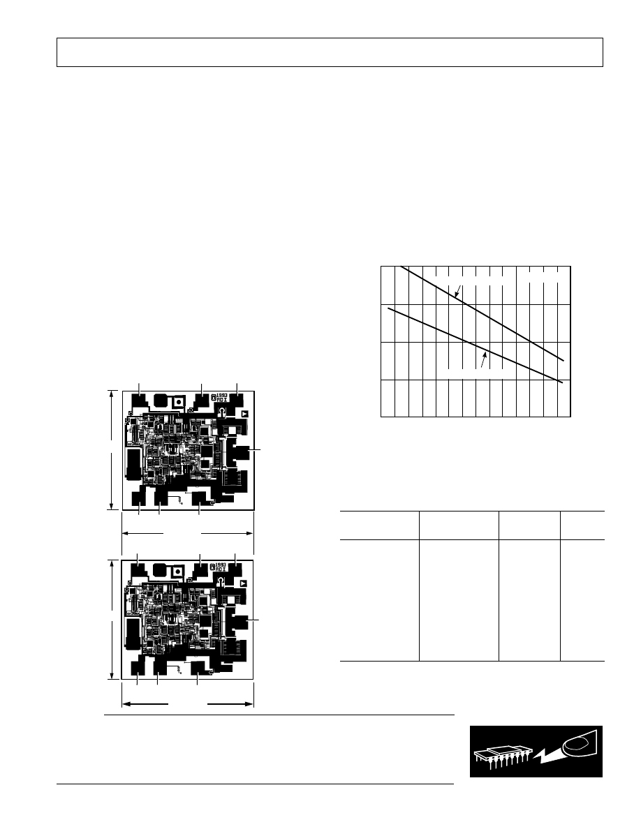
2.0
0
–50
80
1.5
0.5
–40
1.0
0
10
–10
–20
–30
20 30
40
50
60
70
90
AMBIENT TEMPERATURE –
°
C
MAXIMUM POWER DISSIPATION – Watts
T
J
= +150
°
C
8-PIN MINI-DIP PACKAGE
8-PIN SOIC PACKAGE
Figure 2. Plot of Maximum Power Dissipation vs.
Temperature
WARNING!
ESD SENSITIVE DEVICE
CAUTION
ESD (electrostatic discharge) sensitive device. Electrostatic charges as high as 4000 V readily
accumulate on the human body and test equipment and can discharge without detection.
Although these devices feature proprietary ESD protection circuitry, permanent damage may
occur on devices subjected to high energy electrostatic discharges. Therefore, proper ESD
precautions are recommended to avoid performance degradation or loss of functionality.
METALIZATION PHOTO
Dimensions shown in inches and (mm).
Connect Substrate to –V
S
.
ORDERING GUIDE
Temperature
Package
Package
Model
Range
Description Option*
AD8036AN
–40C to +85
°
C
Plastic DIP
N-8
AD8036AR
–40
°
C to +85
°
C
SOIC
R-8
AD8036SQ/883B –55
°
C to +125
°
C
Cerdip
Q-8
AD8036ACHIPS
–40
°
C to +85
°
C
Chips
AD8036-EB
Evaluation
Board
AD8037AN
–40
°
C to +85
°
C
Plastic DIP
N-8
AD8037AR
–40
°
C to +85
°
C
SOIC
R-8
AD8037-EB
Evaluation
Board
*N = Plastic DIP; Q = Cerdip; R= SOIC (Small Outline Integrated Circuit).
AD8036
8 0 3 6
AD8037
8 0 3 7
0.046
(1.17)
3
+IN
4
–V
S
6
OUT
–IN
2
+V
S
7
0.050 (1.27)
0.046
(1.17)
0.050 (1.27)
V
H
8
5
V
L
3
+IN
4
–V
S
6
OUT
–IN
2
+V
S
7
V
H
8
5
V
L
REV. 0
–4–
AD8036/AD8037
+V
S
R
L
= 100
Ω
–V
S
49.9
Ω
V
IN
R
F
130
Ω
V
OUT
0.1
µ
F
10
µ
F
AD8036
0.1
µ
F
10
µ
F
3
2
6
7
4
8
5
PULSE
GENERATOR
T
R
/T
F
= 350ps
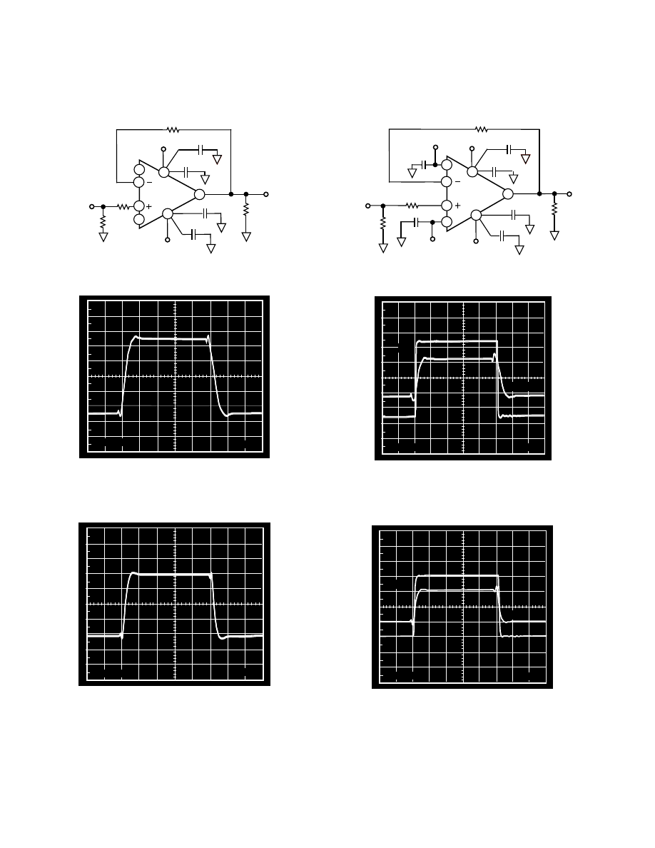
Figure 3. Noninverting Configuration, G = +1
800mV
5ns
Figure 4. Large Signal Transient Response; V
O
= 4 V p-p,
G = +1, R
F
= 140
Ω
100mV
5ns
Figure 5. Small Signal Transient Response; V
O
= 400 mV
p-p, G = +1, R
F
= 140
Ω
AD8036–Typical Characteristics
+V
S
R
L
= 100
Ω
–V
S
V
IN
R
F
V
OUT
0.1
µ
F
10
µ
F
AD8036
0.1
µ
F
10
µ
F
3
2
6
7
4
+V
H
5
0.1
µ
F
PULSE
GENERATOR
T
R
/T
F
= 350ps
49.9
Ω
V
L
0.1
µ
F
130
Ω
8
Figure 6. Noninverting Clamp Configuration, G = +1
800mV
5ns
V
IN
V
OUT
Figure 7. Clamped Large Signal Transient Response (2
×
Overdrive); V
O
= 2 V p-p, G = +1, R
F
= 140
Ω
, V
H
= +1 V,
V
L
= –1 V
5ns
V
OUT
V
IN
200mV
Figure 8. Clamped Small Signal Transient Response (2
×
Overdrive); V
O
= 400 mV p-p, G = +1, R
F
= 140
Ω
, V
H
=
+0.2 V, V
L
= –0.2 V
AD8036/AD8037
REV. 0
–5–
AD8037–Typical Characteristics
+V
S
R
L
= 100
Ω
–V
S
R
F
V
OUT
0.1
µ
F
10
µ
F
AD8037
0.1
µ
F
3
2
6
7
4
8
5
0.1
µ
F
V
L
PULSE
GENERATOR
T
R
/T
F
= 350ps
R
IN
10
µ
F
49.9
Ω
V
IN
100
Ω
0.1
µ
F
V
H
Figure 12. Noninverting Clamp Configuration, G = +2
800mV
5ns
V
IN
V
OUT
Figure 13. Clamped Large Signal Transient Response (2
×
Overdrive); V
O
= 2 V p-p, G = +2, R
F
=
R
IN
= 274
Ω
, V
H
=
+0.5 V, V
L
= –0.5 V
5ns
V
IN
200mV
V
OUT
Figure 14. Clamped Small Signal Transient Response (2
×
Overdrive); V
O
= 400 mV p-p, G = +2, R
F
= R
IN
= 274
Ω
, V
H
=
+0.1 V, V
L
= –0.1 V
+V
S
R
L
= 100
Ω
–V
S
49.9
Ω
V
IN
100
Ω
R
F
V
OUT
0.1
µ
F
10
µ
F
AD8037
0.1
µ
F
10
µ
F
3
2
6
7
4
8
5
PULSE
GENERATOR
T
R
/T
F
= 350ps
R
IN
Figure 9. Noninverting Configuration, G = +2
800mV
5ns
Figure 10. Large Signal Transient Response; V
O
= 4 V p-p,
G = +2, R
F
= R
IN
= 274
Ω
100mV
5ns
Figure 11. Small Signal Transient Response;
V
O
= 400 mV p-p, G = +2, R
F
= R
IN
= 274
Ω
REV. 0
–6–
AD8036/AD8037
AD8036–Typical Characteristics
2
1
0
–1
–2
–3
–4
–5
–6
–7
–8
GAIN – dB
200
Ω
140
Ω
102
Ω
49.9
Ω
1M
FREQUENCY – Hz
10M
100M
1G
V
O
= 300mVp-p
V
S
=
±
5V
R
L
= 100
Ω
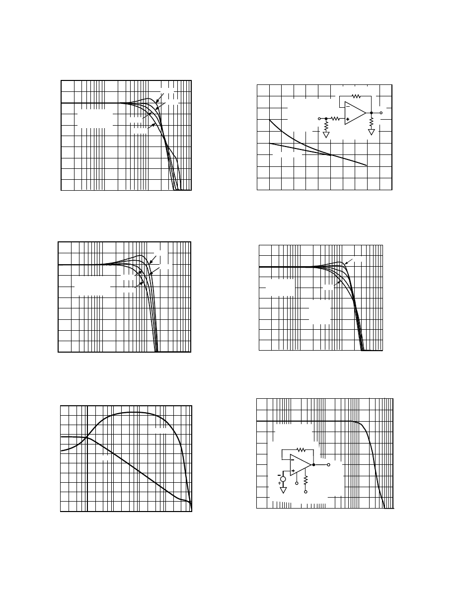
Figure 15. AD8036 Small Signal Frequency Response,
G = +1
0.2
0.1
0
–0.1
–0.2
–0.3
–0.4
–0.5
–0.6
–0.7
–0.8
1M
FREQUENCY – Hz
158
Ω
140
Ω
150
Ω
10M
100M
1G
GAIN – dB
V
O
= 300mVp-p
V
S
=
±
5V
R
L
= 100
Ω
130
Ω
Figure 16. AD8036 0.1 dB Flatness, N Package (for R
Package Add 20
Ω
to R
F
)
60
10
10k
100k
10M
1M
30
20
40
50
FREQUENCY – Hz
OPEN -LOOP GAIN – dB
0
–10
100M
1G
100
20
0
–20
40
60
80
–80
–100
–120
–60
–40
90
70
80
–20
PHASE MARGIN – Degrees
PHASE
GAIN
Figure 17. AD8036 Open-Loop Gain and Phase Margin vs.
Frequency, R
L
= 100
Ω
VALUE OF FEEDBACK RESISTOR (R
F
) –
Ω
–3dB BANDWIDTH – MHz
400
350
300
250
200
20
240
40
200
220
180
160
140
120
100
80
60
R PACKAGE
R
F
130
Ω
AD8036
V
S
=
±
5V
R
L
= 100
Ω
GAIN = +1
R
L
N PACKAGE
49.9
Ω
Figure 18. AD8036 Small Signal –3 dB Bandwidth vs. R
F
2
1
0
–1
–2
–3
–4
–5
–6
–7
–8
OUTPUT – dB
1M
FREQUENCY – Hz
10M
100M
1G
250
Ω
R
F
= 50
Ω
TO
250
Ω
BY
50
Ω
50
Ω
V
S
=
±
5V
V
O
= 2.5Vp-p
R
L
= 100
Ω
Figure 19. AD8036 Large Signal Frequency Response,
G = +1
2
1
0
–1
–2
–3
–4
–5
–6
–7
–8
100k 1M 10M 100M 1G
FREQUENCY – Hz
GAIN – dB
140
Ω
V
H
100
Ω
AD8036
V
L
(V
IN
)
(V
O
)
1V
V
S
=
±
5V
V
O
= 300mVp-p
R
L
= 100
Ω
Figure 20. AD8036 Clamp Input Bandwidth, V
H
, V
L
AD8036/AD8037
REV. 0
–7–
–30
–130
100k
100M
10M
1M
10k
–70
–50
–110
–90
FREQUENCY – Hz
HARMONIC DISTORTION – dBc
V
O
= 2V p-p
V
S
=
±
5V
R
L
= 500
Ω
G = +1
2ND HARMONIC
3RD HARMONIC
Figure 21. AD8036 Harmonic Distortion vs. Frequency,
R
L
= 500
Ω
–30
–130
100k
100M
10M
1M
10k
–70
–50
–110
–90
FREQUENCY – Hz
HARMONIC DISTORTION – dBc
V
O
= 2V p-p
V
S
=
±
5V
R
L
= 100
Ω
G = +1
2ND HARMONIC
3RD HARMONIC
Figure 22. AD8036 Harmonic Distortion vs. Frequency,
R
L
= 100
Ω
50
30
10
100
20
40
FREQUENCY – MHz
INTERCEPT – +dBm
60
20
40
80
60
Figure 23. AD8036 Third Order Intercept vs. Frequency
0.06
0.04
0.02
00.0
–0.02
–0.04
–0.06
DIFF GAIN – %
1st
2nd
3rd
4th
5th
6th
7th
8th
9th 10th 11th
DIFF PHASE – Degrees
1st
2nd
3rd
4th
5th
6th
7th
8th
9th 10th 11th
0.04
0.02
0.00
–0.02
–0.04
Figure 24. AD8036 Differential Gain and Phase Error,
G = +1, R
L
= 150
Ω
, F = 3.58 MHz
SETTLING TIME – ns
0.05
0.04
0.03
0.02
0.01
0
–0.01
–0.02
–0.03
–0.04
–0.05
0 5 10 15 20 25 30 35 40 45
ERROR – %
Figure 25. AD8036 Short-Term Settling Time to 0.01%, 2 V
Step, G = +1, R
L
= 100
Ω
SETTLING TIME -
µ
s
0.4
0.3
0.2
0.1
0
–0.1
–0.2
–0.3
–0.4
–0.5
–0.6
0 2 4 6 8 10 12 14 16 18
ERROR – %
Figure 26. AD8036 Long-Term Settling Time, 2 V Step,
G = +1, R
L
= 100
Ω
REV. 0
–8–
AD8036/AD8037
1M
FREQUENCY – Hz
475
174
374
10M
100M
1G
V
O
= 300mVp-p
V
S
=
±
5V
R
L
= 100
Ω
274
8
7
6
5
4
3
2
1
0
–1
–2
GAIN – dB
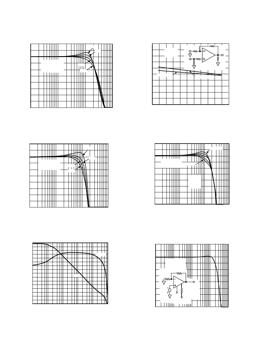
Figure 27. AD8037 Small Signal Frequency Response,
G = +2
301
224
274
V
O
= 3.00m Vp-p
V
S
=
±
5V
R
L
= 100
Ω
249
1M
FREQUENCY – Hz
10M
100M
1G
0.2
0.1
0
–0.1
–0.2
–0.3
–0.4
–0.5
–0.6
–0.7
–0.8
GAIN – dB
Figure 28. AD8037 0.1 dB Flatness, N Package
(for R Package Add 20
Ω
to R
F
)
65
25
–15
10k
100k
1G
100M
10M
1M
35
45
55
–5
5
15
FREQUENCY – Hz
60
20
30
40
50
–10
0
10
OPEN -LOOP GAIN – dB
–50
–250
0
50
100
–200
–150
–100
PHASE MARGIN – Degrees
GAIN
PHASE
Figure 29. AD8037 Open-Loop Gain and Phase Margin
vs. Frequency, R
L
= 100
Ω
AD8037–Typical Characteristics
Figure 30. AD8037 Small Signal –3 dB Bandwidth
vs. R
F
, R
IN
R
F
= 475
Ω
RF = 75
Ω
TO
475
Ω
BY
100
Ω
V
O
= 3.5 Vp-p
V
S
=
±
5V
R
L
= 100
Ω
R
F
= 75
Ω
1M
FREQUENCY – Hz
10M
100M
1G
8
7
6
5
4
3
2
1
0
–1
–2
GAIN – dB
Figure 31. AD8037 Large Signal Frequency Response,
G = +2
100k 1M 10M 100M 1G
FREQUENCY – Hz
GAIN – dB
274
V
H
100
Ω
AD8037
V
L
(V
IN
)
(V
O
)
1V
V
S
=
±
5V
V
O
= 300mVp-p
R
L
= 100
Ω
274
8
7
6
5
4
3
2
1
0
–1
–2
Figure 32. AD8037 Clamp Input Bandwidth, V
H
, V
L
200
150
100
250
300
350
550
500
450
400
350
300
250
200
150
VALUE OF R
F
,R
IN
–
Ω
–3dB BANDWIDTH – MHz
V
S
=
±
5V
R
L
= 100
Ω
GAIN = +2
R
F
AD8037
R
L
R
IN
100
Ω
49.9
Ω
N PACKAGE
R PACKAGE
AD8036/AD8037
REV. 0
–9–
–30
–130
100k
100M
10M
1M
10k
–70
–50
–110
–90
FREQUENCY – Hz
HARMONIC DISTORTION – dBc
V
O
= 2V p-p
V
S
=
±
5V
R
L
= 500
Ω
G = +2
2ND HARMONIC
3RD HARMONIC
Figure 33. AD8037 Harmonic Distortion vs. Frequency,
R
L
= 500
Ω
–30
–130
100k
100M
10M
1M
10k
–70
–50
–110
–90
FREQUENCY – Hz
HARMONIC DISTORTION – dBc
V
O
= 2V p-p
V
S
=
±
5V
R
L
= 100
Ω
G = +2
2ND HARMONIC
3RD HARMONIC
Figure 34. AD8037 Harmonic Distortion vs. Frequency,
R
L
= 100
Ω
50
30
10
100
20
40
FREQUENCY – MHz
INTERCEPT – +dBm
60
20
40
80
60
Figure 35. AD8037 Third Order Intercept vs. Frequency
0.03
0.02
0.01
00.0
–0.01
–0.02
–0.03
DIFF GAIN – %
1st
2nd
3rd
4th
5th
6th
7th
8th
9th 10th 11th
DIFF PHASE – Degrees
1st
2nd
3rd
4th
5th
6th
7th
8th
9th 10th 11th
0.03
0.02
0.01
00.0
–0.01
–0.02
–0.03
Figure 36. AD8037 Differential Gain and Phase Error
G = +2, R
L
= 150
Ω
, F = 3.58 MHz
SETTLING TIME – ns
0.05
0.04
0.03
0.02
0.01
0
–0.01
–0.02
–0.03
–0.04
–0.05
0 5 10 15 20 25 30 35 40 45
ERROR – %
Figure 37. AD8037 Short-Term Settling Time to 0.01%,
2 V Step, G = +2, R
L
= 100
Ω
SETTLING TIME -
µ
s
0.4
0.3
0.2
0.1
0
–0.1
–0.2
–0.3
–0.4
–0.5
–0.6
0 2 4 6 8 10 12 14 16 18
ERROR – %
Figure 38. AD8037 Long-Term Settling Time 2 V Step,
R
L
= 100
Ω
REV. 0
–10–
32
28
24
20
16
12
8
4
100
100k
10k
1k
10
FREQUENCY – Hz
V
S
=
±
5V
INPUT NOISE VOLTAGE – nV/
√
Hz
Figure 39. AD8036 Noise vs. Frequency
80
70
60
50
40
30
20
10
0
75
65
55
45
35
25
15
5
10k
100k
1G
100M
10M
1M
FREQUENCY – Hz
PSRR – dB
–PSRR
+PSRR
Figure 40. AD8036 PSRR vs. Frequency
100
90
80
70
60
50
40
30
20
100k
1G
100M
10M
1M
FREQUENCY – Hz
CMRR – dB
V
S
=
±
5V
∆
V
CM
= 1V
R
L
= 100
Ω
Figure 41. AD8036 CMRR vs. Frequency
AD8036/AD8037–Typical Characteristics
17
13
3
100
100k
10k
1k
10
15
9
11
5
7
FREQUENCY – Hz
INPUT NOISE VOLTAGE – nV/
√
Hz
V
S
=
±
5V
Figure 42. AD8037 Noise vs. Frequency
80
70
60
50
40
30
20
10
0
75
65
55
45
35
25
15
5
10k
100k
1G
100M
10M
1M
FREQUENCY – Hz
PSRR – dB
–PSRR
+PSRR
Figure 43. AD8037 PSRR vs. Frequency
100
90
80
70
60
50
40
30
20
100k
1G
100M
10M
1M
FREQUENCY – Hz
CMRR – dB
V
S
=
±
5V
∆
V
CM
= 1V
R
L
= 100
Ω
Figure 44. AD8037 CMRR vs. Frequency
AD8036/AD8037
REV. 0
–11–
0.1M
FREQUENCY – Hz
1.0M
100M
10M
300M
R
OUT
–
Ω
V
S
=
±
5V
G = +1
1k
100
10
1
0.1
0.01
Figure 45. AD8036 Output Resistance vs. Frequency
0.1M
FREQUENCY – Hz
1.0M
100M
10M
300M
R
OUT
–
Ω
V
S
=
±
5V
G = +2
1k
100
10
1
0.1
0.01
Figure 46. AD8037 Output Resistance vs. Frequency
–60 –40 –20 0 20 40 60 80 100 120 140
OUTPUT SWING – Volts
4.2
4.1
4.0
3.9
3.8
3.7
3.6
3.5
3.4
JUNCTION TEMPERATURE –
°
C
–V
OUT
+V
OUT
R
L
=150
R
L
= 50
–V
OUT
+V
OUT
Figure 47. AD8036/AD8037 Output Swing vs. Temperature
1400
1300
1200
1100
1000
900
800
700
600
500
400
–60 –40 –20 0 20 40 60 80 100 120 140
–A
OL
+A
OL
–A
OL
+A
OL
AD8036
AD8037
JUNCTION TEMPERATURE –
°
C
OPEN -LOOP GAIN – V/ V
Figure 48. Open-Loop Gain vs. Temperature
–60 –40 –20 0 20 40 60 80 100 120 140
PSRR – dB
74
72
70
68
66
64
62
60
JUNCTION TEMPERATURE –
°
C
–PSRR
AD8037
AD8036
AD8037
AD8036
+PSRR
+PSRR
–PSRR
Figure 49. PSRR vs. Temperature
15 25 35 45 55 65 75 85 95
CMRR – dB
96
95
94
93
92
91
90
89
88
JUNCTION TEMPERATURE –
°
C
∆
V
CM
= 2V
Figure 50. AD8036/AD8037 CMRR vs. Temperature
REV. 0
–12–
AD8036/AD8037–Typical Characteristics
–60 –40 –20 0 20 40 60 80 100 120 140
SUPPLY CURRENT – mA
24
23
22
21
20
19
18
17
JUNCTION TEMPERATURE –
°
C
AD8036, V
S
=
±
6V
AD8036, V
S
=
±
5V
AD8037, V
S
=
±
6V
AD8037, V
S
=
±
5V
Figure 51. Supply Current vs. Temperature
–60 –40 –20 0 20 40 60 80 100 120 140
JUNCTION TEMPERATURE –
°
C
V
S
=
±
6V
V
S
=
±
5V
V
S
=
±
6V
V
S
=
±
5V
INPUT OFFSET VOLTAGE – mV
–2.50
–2.25
–2.00
–1.75
–1.50
–1.25
–1.00
–0.75
–0.50
AD8037
AD8036
Figure 52. Input Offset Voltage vs. Temperature
44
40
36
32
28
24
20
16
12
8
4
0
–6 –5 –4 –3 –2 –1 0 1 2 3 4
INPUT OFFSET VOLTAGE – mV
COUNT
3 WAFER LOTS
COUNT = 632
FREQ. DIST
Figure 53. AD8036 Input Offset Voltage Distribution
–60 –40 –20 0 20 40 60 80 100 120 140
270
260
250
240
230
220
210
200
JUNCTION TEMPERATURE –
°
C
AD8037
AD8036
AD8036
SHORT CIRCUIT CURRENT – mA
AD8037
SINK
SOURCE
Figure 54. Short Circuit Current vs. Temperature
–60 –40 –20 0 20 40 60 80 100 120 140
JUNCTION TEMPERATURE –
°
C
–IB
INPUT BIAS CURRENT – µA
AD8037
AD8036
+IB
–IB
+IB
4.5
4.0
3.5
3.0
2.5
2.0
1.5
Figure 55. Input Bias Current vs. Temperature
–4.5 –4.0 –3.5 –3.0 –2.5 –2.0 –1.5 –1.0 –.5 0 .5
INPUT OFFSET VOLTAGE – mV
COUNT
3 WAFER LOTS
COUNT = 853
FREQ. DIST
48
44
40
36
32
28
24
20
16
12
8
4
0
Figure 56. AD8037 Input Offset Voltage Distribution
REV. 0
–13–
0.6 0.65 0.7 0.75 0.8 0.85 0.9 0.95 1.0
–80
–75
–70
–65
–60
–55
–50
–45
–40
–35
–30
ABSOLUTE VALUE OF OUTPUT VOLTAGE – Volts
HARMONIC DISTORTION – dBc
V
H
+1V +0.5V
V
L
–1V –0.5V
G +1V +2V
AD8036 AD8037
AD8037 3RD
HARMONIC
AD8036 3RD
HARMONIC
AD8036 2ND
HARMONIC
AD8037 2ND
HARMONIC
Figure 60. Harmonic Distortion as Output Approaches
Clamp Voltage; V
O
= 2 V p-p, R
L
= 100
Ω
, f = 20 MHz
–5 –4 –3 –2 –1 0 1 2 3 4 5
80
60
40
20
0
–20
–40
–60
–80
INPUT CLAMP VOLTAGE (V
H
,V
L
) – Volts
I
BH
I
BL
POSITIVE I
BH
, I
BL
DENOTES
CURRENT FLOW INTO
CLAMP INPUTS V
H
, V
L
CLAMP INPUT BIAS CURRENT – µA
Figure 61. AD8036/AD8037 Clamp Input Bias Current vs.
Input Clamp Voltage
REF
+2V
+1V
0V
10mV
1ns
Figure 62. AD8037 Clamp Overdrive (2X) Recovery
–3 –2 –1 0 1 2 3
20
15
10
5
0
–5
–10
–15
–20
OUTPUT VOLTAGE – Volts
AD8036, A
CL
=+1
AD8037, A
CL
=+2
V
CL
= –3V
V
CL
= –2V
V
CL
= –1V
V
CH
= +1V
V
CH
= +2V
V
CH
= +3V
AD8036
AD8037
INPUT ERROR VOLTAGE – mV
Figure 57. Input Error Voltage vs. Clamped Output
Voltage
1.0
–0.8
–1.0
0.8
0.6
0.4
0.2
0.0
–0.2
–0.4
–0.6
20
15
10
5
0
–5
–10
–15
–20
INPUT VOLTAGE * A
V
– Volts
LINEARITY – mV
V
H
= + 1V
V
L
= – 1V
Figure 58. AD8036/AD8037 Nonlinearity Near Clamp
Voltage
REF
+2V
+1V
0V
10mV
1ns
Figure 59. AD8036 Clamp Overdrive (2X) Recovery
Clamp Characteristics–AD8036/AD8037
AD8036/AD8037–Clamp Characteristics
REV. 0
–14–
0.5
0.4
0.3
0.2
0.1
0
–0.1
–0.2
–0.3
–0.4
–0.5
0 10 20 30 40 50 60 70 80 90
ERROR – %
SETTLING TIME – ns
Figure 66. AD8037 Clamp Settling (0.1%), V
H
= +0.5 V,
V
L
= –0.5 V, 2X Overdrive
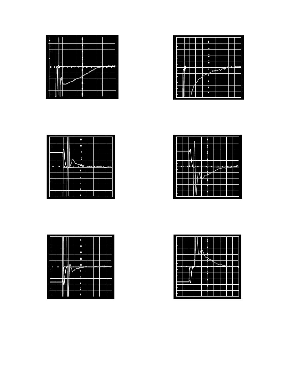
0.5
0.4
0.3
0.2
0.1
0
–0.1
–0.2
–0.3
–0.4
–0.5
0 5 10 15 20 25 30 35 40
ERROR – %
SETTLING TIME – ns
Figure 67. AD8037 Clamp Recovery Settling Time (High),
from +2X Overdrive to 0 V
0.5
0.4
0.3
0.2
0.1
0
–0.1
–0.2
–0.3
–0.4
–0.5
0 5 10 15 20 25 30 35 40
ERROR – %
SETTLING TIME – ns
Figure 68. AD8037 Clamp Recovery Settling Time (Low),
from –2X Overdrive to 0 V
0.5
0.4
0.3
0.2
0.1
0
–0.1
–0.2
–0.3
–0.4
–0.5
0 10 20 30 40 50 60 70 80 90
ERROR – %
SETTLING TIME – ns
Figure 63. AD8036 Clamp Settling (0.1%), V
H
= +1 V,
V
L
= –1 V, 2X Overdrive
0.5
0.4
0.3
0.2
0.1
0
–0.1
–0.2
–0.3
–0.4
–0.5
0 5 10 15 20 25 30 35 40
ERROR – %
SETTLING TIME – ns
Figure 64. AD8036 Clamp Recovery Settling Time (High),
from +2X Overdrive to 0 V
0.5
0.4
0.3
0.2
0.1
0
–0.1
–0.2
–0.3
–0.4
–0.5
0 5 10 15 20 25 30 35 40
ERROR – %
SETTLING TIME – ns
Figure 65. AD8036 Clamp Recovery Settling Time (Low),
from –2X Overdrive to 0 V
AD8036/AD8037
REV. 0
–15–
THEORY OF OPERATION
General
The AD8036 and AD8037 are wide bandwidth, voltage feed-
back clamp amplifiers. Since their open-loop frequency re-
sponse follows the conventional 6 dB/octave roll-off, their gain
bandwidth product is basically constant. Increasing their
closed-loop gain results in a corresponding decrease in small sig-
nal bandwidth. This can be observed by noting the bandwidth
specification, between the AD8036 (gain of 1) and AD8037
(gain of 2). The AD8036/AD8037 typically maintain 65 de-
grees of phase margin. This high margin minimizes the effects
of signal and noise peaking.
While the AD8036 and AD8037 can be used in either an invert-
ing or noninverting configuration, the clamp function will only
work in the noninverting mode. As such, this section shows con-
nections only in the noninverting configuration. Applications
that require an inverting configuration will be discussed in the
Applications section. In applications that do not require clamp-
ing, Pins 5 and 8 (respectively V
L
and V
H
) may be left floating.
See Input Clamp Amp Operation and Applications sections oth-
erwise.
Feedback Resistor Choice
The value of the feedback resistor is critical for optimum perfor-
mance on the AD8036 (gain +1) and less critical as the gain in-
creases. Therefore, this section is specifically targeted at the
AD8036.
At minimum stable gain (+1), the AD8036 provides optimum
dynamic performance with R
F
= 140
Ω
. This resistor acts only
as a parasitic suppressor against damped RF oscillations that
can occur due to lead (input, feedback) inductance and parasitic
capacitance. This value of R
F
provides the best combination of
wide bandwidth, low parasitic peaking, and fast settling time.
In fact, for the same reasons, a 100–130
Ω
resistor should be
placed in series with the positive input for other AD8036
noninverting configurations. The correct connection is shown in
Figure 69.
+V
S
R
TERM
V
IN
R
F
100 - 130
Ω
V
OUT
0.1
µ
F
10
µ
F
AD8036/37
0.1
µ
F
R
F
R
G
G =1+
10
µ
F
R
G
3
2
6
7
4
8
5
–V
S
V
H
V
L
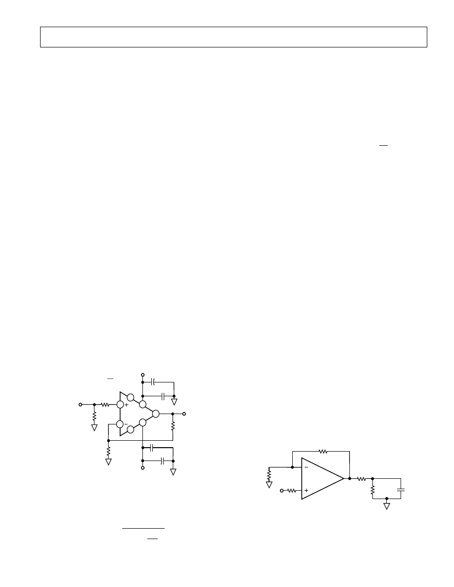
Figure 69. Noninverting Operation
For general voltage gain applications, the amplifier bandwidth
can be closely estimated as:
f
3 dB
≅
ω
O
2
π
1
+
R
F
R
G
This estimation loses accuracy for gains of +2/–1 or lower due
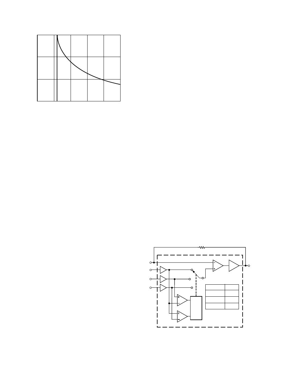
to the amplifier’s damping factor. For these “low gain” cases,
the bandwidth will actually extend beyond the calculated value
(see Closed-Loop BW plots, Figures 15 and 27).
Pulse Response
Unlike a traditional voltage feedback amplifier, where the slew
speed is dictated by its front end dc quiescent current and gain
bandwidth product, the AD8036 and AD8037 provide “on de-
mand” current that increases proportionally to the input “step”
signal amplitude. This results in slew rates (1200 V/
µ
s) compa-
rable to wideband current feedback designs. This, combined
with relatively low input noise current (2.1 pA/
√
Hz
), gives the
AD8036 and AD8037 the best attributes of both voltage and
current feedback amplifiers.
Large Signal Performance
The outstanding large signal operation of the AD8036 and
AD8037 is due to a unique, proprietary design architecture.
In order to maintain this level of performance, the maximum
350 V-MHz product must be observed, (e.g., @ 100 MHz,
V
O
≤
3.5 V p-p).
Power Supply and Input Clamp Bypassing
Adequate power supply bypassing can be critical when optimiz-
ing the performance of a high frequency circuit. Inductance in
the power supply leads can form resonant circuits that produce
peaking in the amplifier’s response. In addition, if large current
transients must be delivered to the load, then bypass capacitors
(typically greater than 1
µ
F) will be required to provide the best
settling time and lowest distortion. A parallel combination of at
least 4.7
µ
F, and between 0.1
µ
F and 0.01
µ
F, is recommended.
Some brands of electrolytic capacitors will require a small series
damping resistor
≈
4.7
Ω
for optimum results.
When the AD8036 and AD8037 are used in clamping mode,
and a dc voltage is connected to clamp inputs V
H
and V
L
, a 0.1
µ
F
bypassing capacitor is required between each input pin and
ground in order to maintain stability.
Driving Capacitive Loads
The AD8036 and AD8037 were designed primarily to drive
nonreactive loads. If driving loads with a capacitive component
is desired, the best frequency response is obtained by the addi-
tion of a small series resistance as shown in Figure 70. The ac-
companying graph shows the optimum value for R
SERIES
vs.
capacitive load. It is worth noting that the frequency response of
the circuit when driving large capacitive loads will be dominated
by the passive roll-off of R
SERIES
and C
L
. For capacitive loads of
6 pF or less, no R
SERIES
is necessary.
R
L
1k
Ω
AD8036/37
R
F
R
IN
R
IN
R
SERIES
C
L
Figure 70. Driving Capacitive Loads
REV. 0
–16–
AD8036/AD8037
Operation of the AD8036 for negative input voltages and nega-
tive clamp levels on V
L
is similar, with comparator C
L
control-
ling S1. Since the comparators see the voltage on the +V
IN
pin
as their common reference level, then the voltage V
H
and V
L
are
defined as “High” or “Low” with respect to +V
IN
. For example,
if V
IN
is set to zero volts, V
H
is open, and V
L
is +1 V, compara-
tor C
L
will switch S1 to “C,” so the AD8036 will buffer the
voltage on V
L
and ignore +V
IN
.
The performance of the AD8036 and AD8037 closely matches
the ideal just described. The comparator’s threshold extends
from 60 mV inside the clamp window defined by the voltages on
V
L
and V
H
to 60 mV beyond the window’s edge. Switch S1 is
implemented with current steering, so that A1’s +input makes a
continuous transition from say, V
IN
to V
H
as the input voltage
traverses the comparator’s input threshold from 0.9 V to 1.0 V
for V
H
= 1.0 V.
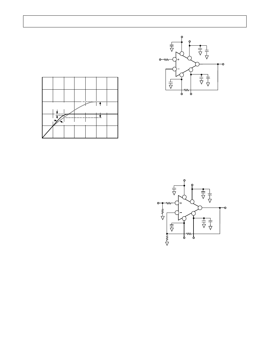
The practical effect of these nonidealities is to soften the
transition from amplification to clamping modes, without com-
promising the absolute clamp limit set by the CLAMPIN cir-
cuit. Figure 73 is a graph of V
OUT
vs. V
IN
for the AD8036 and a
typical output clamp amplifier. Both amplifiers are set for G =
+1 and V
H
= +1 V.
The worst case error between V
OUT
(ideally clamped) and V
OUT
(actual) is typically 18 mV times the amplifier closed-loop gain.
This occurs when V
IN
equals V
H
(or V
L
). As V
IN
goes above
and/or below this limit, V
OUT
will settle to within 5 mV of the
ideal value.
In contrast, the output clamp amplifier’s transfer curve typically
will show some compression starting at an input of 0.8 V, and
can have an output voltage as far as 200 mV over the clamp
limit. In addition, since the output clamp in effect causes the
amplifier to operate open loop in clamp mode, the amplifier’s
output impedance will increase, potentially causing additional
errors.
The AD8036’s and AD8037’s CLAMPIN input clamp architec-
ture works only for noninverting or follower applications and,
since it operates on the input, the clamp voltage levels V
H
and
V
L
, and input error limits will be multiplied by the amplifier’s
A1
A2
+1
A
B
C
C
H
C
L
+1
+1
+1
S1
R
F
140
Ω
A B C
0 1 0
1 0 0
0 0 1
S1
V
IN
> V
H
V
L
≤
V
IN
≤
V
H
V
IN
< V
L
–V
IN
+V
IN
V
H
V
L
V
OUT
Figure 72. AD8036/AD8037 Clamp Amp System
0 5 10 15 20 25
R
SERIES
–
Ω
C
L
–pF
40
30
20
10
Figure 71. Recommended R
SERIES
vs. Capacitive Load
INPUT CLAMPING AMPLIFIER OPERATION
The key to the AD8036 and AD8037’s fast, accurate clamp and
amplifier performance is their unique patent pending CLAMPIN
input clamp architecture. This new design reduces clamp errors
by more than 10
×
over previous output clamp based circuits, as
well as substantially increasing the bandwidth, precision and
versatility of the clamp inputs.
Figure 72 is an idealized block diagram of the AD8036 con-
nected as a unity gain voltage follower. The primary signal path
comprises A1 (a 1200 V/
µ
s, 240 MHz high voltage gain, differ-
ential to single-ended amplifier) and A2 (a G = +1 high current
gain output buffer). The AD8037 differs from the AD8036 only
in that A1 is optimized for closed-loop gains of two or greater.
The CLAMPIN section is comprised of comparators C
H
and
C
L
, which drive switch S1 through a decoder. The unity-gain
buffers in series with +V
IN
, V
H
, and V
L
inputs isolate the input
pins from the comparators and S1 without reducing bandwidth
or precision.
The two comparators have about the same bandwidth as A1
(240 MHz), so they can keep up with signals within the useful
bandwidth of the AD8036. To illustrate the operation of the
CLAMPIN circuit, consider the case where V
H
is referenced to
+1 V, V
L
is open, and the AD8036 is set for a gain of +1, by
connecting its output back to its inverting input through the rec-
ommended 140
Ω
feedback resistor. Note that the main signal
path always operates closed loop, since the CLAMPIN circuit
only affects A1’s noninverting input.
If a 0 V to +2 V voltage ramp is applied to the AD8036’s +V
IN
for the connection just described, V
OUT
should track +V
IN
per-
fectly up to +1 V, then should limit at exactly +1 V as +V
IN
con-
tinues to +2 V.
In practice, the AD8036 comes close to this ideal behavior. As
the +V
IN
input voltage ramps from zero to 1 V, the output of the
high limit comparator C
H
starts in the off state, as does the out-
put of C
L
. When +V
IN
just exceeds V
IN
(ideally, by say 1
µ
V,
practically by about 18 mV), C
H
changes state, switching S1
from “A” to “B” reference level. Since the + input of A1 is now
connected to V
H
, further increases in +V
IN
have no effect on the
AD8036’s output voltage. In short, the AD8036 is now operat-
ing as a unity-gain buffer for the V
H
input, as any variation in
V
H
, for V
H
> 1 V, will be faithfully reproduced at V
OUT
.
AD8036/AD8037
REV. 0
–17–
closed-loop gain at the output. For instance, to set an output
limit of
±
1 V for an AD8037 operating at a gain of 3.0, V
H
and
V
L
would need to be set to +0.333 V and –0.333 V, respectively.
The only restriction on using the AD8036’s and AD8037’s
+V
IN
, V
L
, V
H
pins as inputs is that the maximum voltage differ-
ence between +V
IN
and V
H
or V
L
should not exceed 6.3 V, and
all three voltages be within the supply voltage range. For ex-
ample, if V
L
is set at –3 V, then V
IN
should not exceed +3.3 V.
0.6 0.8 1.0 1.2 1.4 1.6 1.8 2.0
INPUT VOLTAGE – +V
IN
1.6
0.6
1.2
0.8
1.0
1.4
OUTPUT VOLTAGE – V
OUT
AD8036
OUTPUT CLAMP AMP
CLAMP ERROR – 25mV
AD8036
CLAMP ERROR – >200mV
OUTPUT CLAMP
Figure 73. Output Clamp Error vs. Input Clamp Error
AD8036/AD8037 APPLICATIONS
The AD8036 and AD8037 use a unique input clamping circuit
to perform the clamping function. As a result, they provide the
clamping function better than traditional output clamping de-
vices and provide additional flexibility to perform other unique
applications.
There are, however, some restrictions on circuit configurations;
and some calculations need to be performed in order to figure
the clamping level, as a result of clamping being performed at
the input stage.
The major restriction on the clamping feature of the AD8036/
AD8037 is that clamping occurs only when using the amplifiers
in the noninverting mode. To clamp in an inverting circuit, an
additional inverting gain stage is required. Another restriction is
that V
H
be greater than V
L
, and that each be within the output
voltage range of the amplifier (
±
3.9 V). V
H
can go below ground
and V
L
can go above ground as long as V
H
is kept higher than V
L
.
Unity Gain Clamping
The simplest circuit for calculating the clamp levels is a unity
gain follower as shown in Figure 74. In this case, the AD8036
should be used since it is compensated for noninverting unity
gain.
This circuit will clamp at an upper voltage set by V
H
(the voltage
applied to Pin 8) and a lower voltage set by V
L
(the voltage ap-
plied to Pin 5).
Clamping with Gain
Figure 75 shows an AD8037 configured for a noninverting gain
of two. The AD8037 is used in this circuit since it is compen-
sated for gains of two or greater and provides greater band-
width. In this case, the high clamping level at the output will
+5V
V
IN
R
F
130
Ω
V
OUT
10µF
AD8036
0.1µF
3
6
7
4
8
5
–5V
V
H
+
+
V
L
140
Ω
V
L
2
V
H
UNITY GAIN NONINVERTING CLAMP
0.1µF
0.1µF
0.1µF
10µF
Figure 74. Unity Gain Noninverting Clamp
occur at 2
×
V
H
and the low clamping level at the output will be
2
×
V
L
. The equations governing the output clamp levels in cir-
cuits configured for noninverting gain are:
V
CH
= G
×
V
H
V
CL
= G
×
V
L
where:
V
CH
is the high output clamping level
V
CL
is the low output clamping level
G is the gain of the amplifier configuration
V
H
is the high input clamping level (Pin 8)
V
L
is the low input clamping level (Pin 5)
*Amplifier offset is assumed to be zero.
+5V
V
IN
R
F
100
Ω
V
OUT
10µF
AD8037
0.1µF
3
6
7
4
8
5
–5V
V
H
+
+
V
L
274
Ω
V
L
2
V
H
0.1µF
274
Ω
R
G
49.9
Ω
GAIN OF TWO NONINVERTING CLAMP
0.1µF
10µF
0.1µF
Figure 75. Gain of Two Noninverting Clamp
Clamping with an Offset
Some op amp circuits are required to operate with an offset
voltage. These are generally configured in the inverting mode
where the offset voltage can be summed in as one of the inputs.
Since AD8036/AD8037 clamping does not function in the in-
verting mode, it is not possible to clamp with this configuration.
Figure 76 shows a noninverting configuration of an AD8037
that provides clamping and also has an offset. The circuit shows
the AD8037 as a driver for an AD9002, an 8-bit, 125 Msps
A/D converter and illustrates some of the considerations for us-
ing an AD8037 with offset and clamping.
REV. 0
–18–
AD8036/AD8037
The analog input range of the AD9002 is from ground to –2 V.
The input should not go more than 0.5 V outside this range in
order to prevent disruptions to the internal workings of the A/D
and to avoid drawing excess current. These requirements make
the AD8037 a prime candidate for signal conditioning.
When an offset is added to a noninverting op amp circuit, it is
fed in through a resistor to the inverting input. The result is that
the op amp must now operate at a closed-loop gain greater than
unity. For this circuit a gain of two was chosen which allows the
use of the AD8037. The feedback resistor, R2, is set at 301
Ω
for optimum performance of the AD8037 at a gain of two.
There is an interaction between the offset and the gain, so some
calculations must be performed to arrive at the proper values for
R1 and R3. For a gain of two the parallel combination of resis-
tors R1 and R3 must be equal to the feedback resistor R2. Thus
R1
×
R3/R1 + R3 = R2 = 301
Ω
The reference used to provide the offset is the AD780 whose
output is 2.5 V. This must be divided down to provide the 1 V
offset desired. Thus
2.5 V
×
R1/(R1 + R3) = 1 V
When the two equations are solved simultaneously we get R1 =
499
Ω
and R3 = 750
Ω
(using closest 1% resistor values in all
cases). This positive 1 V offset at the input translates to a –1 V
offset at the output.
The usable input signal swing of the AD9002 is 2 V p-p. This is
centered about the –1 V offset making the usable signal range
from 0 V to –2 V. It is desirable to clamp the input signal so
that it goes no more than 100 mV outside of this range in either
direction. Thus, the high clamping level should be set at +0.1 V
and the low clamping level should be set at –2.1 V as seen at the
input of the AD9002 (output of AD8037).
Because the clamping is done at the input stage of the AD8037,
the clamping level as seen at the output is affected by not only
the gain of the circuit as previously described, but also by the
offset. Thus, in order to obtain the desired clamp levels, V
H
must be biased at +0.55 V while V
L
must be biased at –0.55 V.
The clamping levels as seen at the output can be calculated by
the following:
V
CH
= V
OFF
+ G
×
V
H
V
CL
= V
OFF
+ G
×
V
L
Where V
OFF
is the offset voltage that appears at the output.
The resistors used to generate the voltages for V
H
and V
L
should
be kept to a minimum in order to reduce errors due to clamp
bias current. This current is dependent on V
H
and V
L
(see Fig-
ure 61) and will create a voltage drop across whatever resistance
is in series with each clamp input. This extra error voltage is
multiplied by the closed-loop gain of the amplifier and can be
substantial, especially in high closed-loop gain configurations. A
0.1
µ
F bypass capacitor should be placed between input clamp
pins V
H
and V
L
and ground to ensure stable operation.
The 1N5712 Schottky diode is used for protection from forward
biasing the substrate diode in the AD9002 during power-up
transients.
Programmable Pulse Generator
The AD8036/AD8037’s clamp output can be set accurately and
has a well controlled flat level. This along with wide bandwidth
and high slew rate make them very well suited for programmable
level pulse generators.
Figure 77 is a schematic for a pulse generator that can directly
accept TTL generated timing signals for its input and generate
pulses at the output up to 24 V p-p with 2500 V/
µ
s slew rate.
The output levels can be programmed to anywhere in the range
–12 V to +12 V.
The circuit uses an AD8037 operating at a gain of two with an
AD811 to boost the output to the
±
12 V range. The AD811 was
chosen for its ability to operate with
±
15 V supplies and its high
slew rate.
R1 and R2 act as a level shifter to make the TTL signal levels be
approximately symmetrical above and below ground. This en-
sures that both the high and low logic levels will be clamped by
the AD8037. For well controlled signal levels in the output
pulse, the high and low output levels should result from the
clamping action of the AD8037 and not be controlled by either
+5V
V
IN
R2
100
Ω
AD8037
3
6
7
4
8
5
–5V
+
+
301
Ω
V
L
2
V
H
GAIN OF TWO, NONINVERTING WITH OFFSET AD8037
DRIVING AN AD9002 – 8-BIT, 125 MSPS A/D CONVERTER
806
Ω
100
Ω
+5V
49.9
Ω
750
Ω
–0.5V to +0.5V
0.1µF
0.1µF
10µF
R3
100
Ω
0.1
µF
806
Ω
–5V
49.9
Ω
–2V to 0V
CLAMPING
RANGE
–2.1V to +0.1V
499
Ω
R1
0.1
µF
2.5V
AD780
+5V
+
0.1
µF
10µF
AD9002
VIN= –2V TO 0V
SUBSTRATE
DIODE
–5.2V
0.1µF
1N5712
0.1µF
10µF
Figure 76. Gain of Two, Noninverting with Offset AD8037 Driving an AD9002—8-Bit, 125 MSPS A/D Converter
AD8036/AD8037
REV. 0
–19–
the high or low logic levels passing through a linear amplifier.
For good rise and fall times at the output pulse, a logic family
with high speed edges should be used.
The high logic levels are clamped at two times the voltage at V
H
,
while the low logic levels are clamped at two times the voltage
at V
L
. The output of the AD8037 is amplified by the AD811
operating at a gain of 5. The overall gain of 10 will cause the
high output level to be 10 times the voltage at V
H
, and the low
output level to be 10 times the voltage at V
L
.
High Speed, Full-Wave Rectifier
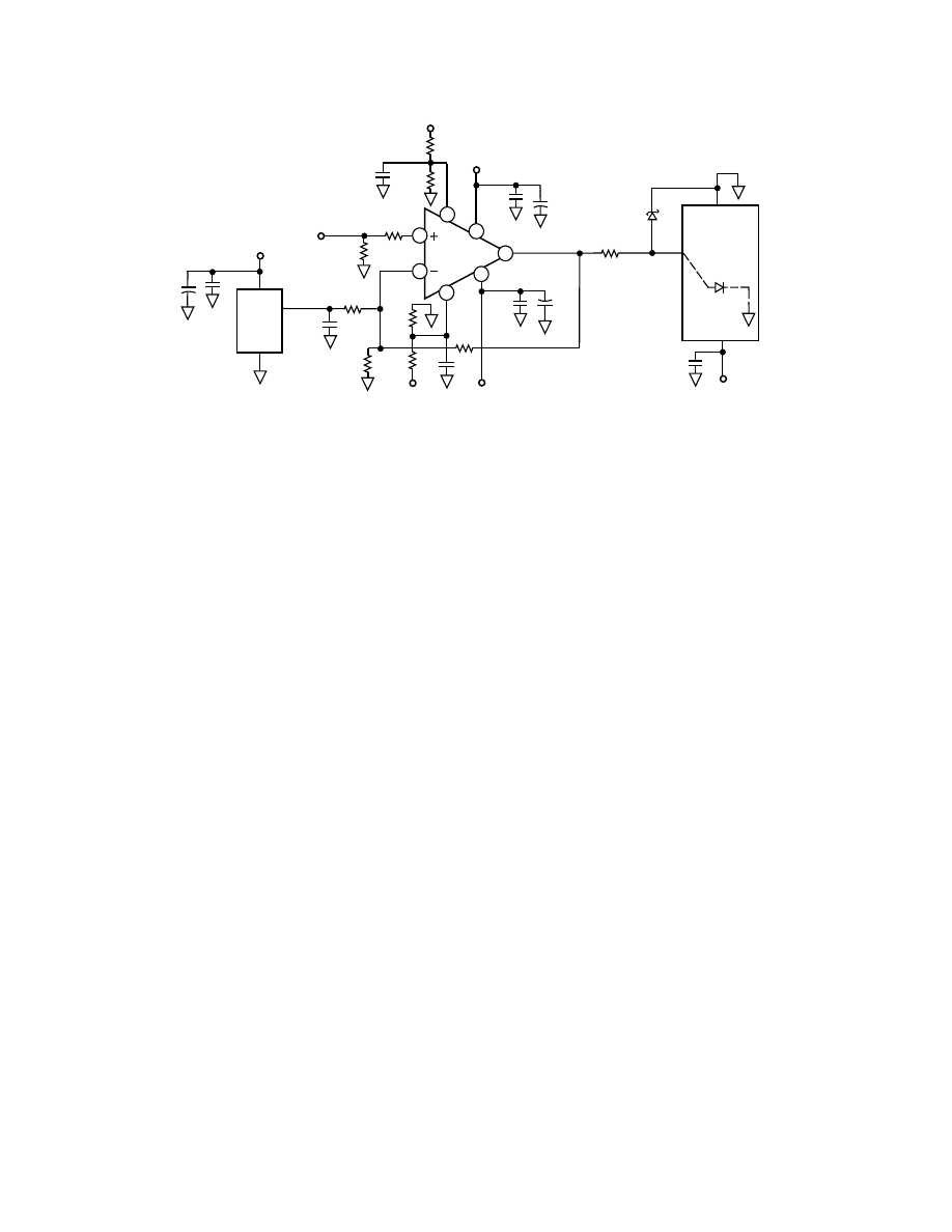
The clamping inputs are additional inputs to the input stage of
the op amp. As such they have an input bandwidth comparable
to the amplifier inputs and lend themselves to some unique
functions when they are driven dynamically.
Figure 78 is a schematic for a full-wave rectifier, sometimes
called an absolute value generator. It works well up to 20 MHz
and can operate at significantly higher frequencies with some
degradation in performance. The distortion performance is sig-
nificantly better than diode based full-wave rectifiers, especially
at high frequencies.
+5V
100
Ω
10µF
AD8037
3
6
7
4
8
5
–5V
+
+
274
Ω
V
L
2
V
H
FULL-WAVE RECTIFIER
0.1µF
R
F
R
G
274
Ω
V
IN
V
OUT =
V
IN
10µF
0.1µF
Figure 78. Full-Wave Rectifier
The circuit is configured as an inverting amplifier with a gain
of one. The input drives the inverting amplifier and also directly
drives V
L
, the lower level clamping input. The high level clamp-
ing input, V
H
, is left floating and plays no role in this circuit.
+5V
TTL
IN
200
Ω
10µF
AD8037
3
6
7
4
8
5
–5V
V
H
+
10µF
+
V
L
274
Ω
V
L
2
V
H
274
Ω
1.3k
PROGRAMMABLE PULSE GENERATOR
+
–15V
100
Ω
AD811
150
Ω
3
6
7
4
1
5
2
604
Ω
+
+15V
0.1µF
10µF
PLUSE
OUT
VH X 10
VL X 10
–15V
0.1µF
0.1µF
0.1µF
10µF
0.1µF
0.1µF
Figure 77. Programmable Pulse Generator
When the input is negative, the amplifier acts as a regular unity-
gain inverting amplifier and outputs a positive signal at the same
amplitude as the input with opposite polarity. V
L
is driven nega-
tive by the input, so it performs no clamping action, because the
positive output signal is always higher than the negative level
driving V
L
.
When the input is positive, the output result is the sum of two
separate effects. First, the inverting amplifier multiplies the in-
put by –1 because of its unity-gain inverting configuration. This
effectively produces an offset as explained above, but with a dy-
namic level that is equal to –1 times the input.
Second, although the positive input is grounded (through 100
Ω
),
the output is clamped at two times the voltage applied to V
L
(a
positive, dynamic voltage in this case). The factor of two is be-
cause the noise gain of the amplifier is two.
The sum of these two actions results in an output that is equal
to unity times the input signal for positive input signals, see Fig-
ure 79. For a input/output scope photo with an input signal of
20 MHz and amplitude
±
1 V, see Figure 80.
INPUT
FULL WAVE
RECTIFIED
OUTPUT
LOWER
CLAMPING
LEVEL WITH
NO NEG INPUT
OUTPUT
LOWER
CLAMPING
LEVEL
–1 X INPUT
Figure 79.
REV. 0
–20–
AD8036/AD8037
500mV
20ns
500mV
90
100
0%
10
Figure 80. Full-Wave Rectifier Scope
Thus for either positive or negative input signals, the output is
unity times the absolute value of the input signal. The circuit
can be easily configured to produce the negative absolute value
of the input by applying the input to V
H
instead of V
L
.
The circuit can get to within about 40 mV of ground during the
time when the input crosses zero. This voltage is fixed over a
wide frequency range and is a result of the switching between
the conventional op amp input and the clamp input. But be-
cause there are no diodes to rapidly switch from forward to re-
verse bias, the performance far exceeds that of diode based full
wave rectifiers.
The 40 mV offset mentioned can be removed by adding an off-
set to the circuit. A 27.4 k
Ω
input resistor to the inverting input
will have a gain of 0.01, while changing the gain of the circuit by
only 1%. A plus or minus 4 V dc level (depending on the polar-
ity of the rectifier) into this resistor will compensate for the
offset.
Full wave rectifiers are useful in many applications including
AM signal detection, high frequency ac voltmeters and various
arithmetic operations.
Amplitude Modulator
In addition to being able to be configured as an amplitude de-
modulator (AM detector), the AD8037 can also be configured
as an amplitude modulator as shown in Figure 81.
+5V
CARRIER IN
100
Ω
10µF
AD8037
3
6
7
4
8
5
–5V
V
H
+
10
µF
+
274
Ω
V
L
2
V
H
AMPLITUDE MODULATOR
0.1µF
R
F
R
G
274
Ω
AM OUT
MODULATION IN
0.1
µF
Figure 81. Amplitude Modulator
The positive input of the AD8037 is driven with a square wave
of sufficient amplitude to produce clamping action at both the
high and low levels. This is the higher frequency carrier signal.
The modulation signal is applied to both the input of a unity
gain inverting amplifier and to V
L
, the lower clamping input.
V
H
is biased at +0.5 V dc.
To understand the circuit operation, it is helpful to first con-
sider a simpler circuit. If both V
L
and
V
H
were dc biased at
–0.5 V and the carrier and modulation inputs driven as above,
the output would be a 2 V p-p square wave at the carrier fre-
quency riding on a waveform at the modulating frequency. The
inverting input (modulation signal) is creating a varying offset to
the 2 V p-p square wave at the output. Both the high and low
levels clamp at twice the input levels on the clamps because the
noise gain of the circuit is two.
When V
L
is driven by the modulation signal instead of being
held at a dc level, a more complicated situation results. The re-
sulting waveform is composed of an upper envelope and a lower
envelope with the carrier square wave in between. The upper
and lower envelope waveforms are 180
°
out of phase as in a
typical AM waveform.
The upper envelope is produced by the upper clamp level being
offset by the waveform applied to the inverting input. This offset
is the opposite polarity of the input waveform because of the
inverting configuration.
The lower envelope is produced by the sum of two effects. First,
it is offset by the waveform applied to the inverting input as in
the case of the simplified circuit above. The polarity of this off-
set is in the same direction as the upper envelope. Second, the
output is driven in the opposite direction of the offset at twice
the offset voltage by the modulation signal being applied to V
L
.
This results from the noise gain being equal to two, and since
there is no inversion in this connection, it is opposite polarity
from the offset.
The result at the output for the lower envelope is the sum of
these two effects, which produces the lower envelope of an am-
plitude modulated waveform. See Figure 82.
AM WAVEFORM
Figure 82. AM Waveform
The depth of modulation can be modified in this circuit by
changing the amplitude of the modulation signal. This changes
the amplitude of the upper and lower envelope waveforms.
The modulation depth can also be changed by changing the dc
bias applied to V
H
. In this case the amplitudes of the upper and
lower envelope waveforms stay constant, but the spacing be-
tween them changes. This alters the ratio of the envelope ampli-
tude to the amplitude of the overall waveform.
AD8036/AD8037
REV. 0
–21–
Layout Considerations
The specified high speed performance of the AD8036 and
AD8037 requires careful attention to board layout and compo-
nent selection. Proper RF design techniques and low pass para-
sitic component selection are mandatory.
The PCB should have a ground plane covering all unused por-
tions of the component side of the board to provide a low im-
pedance path. The ground plane should be removed from the
area near the input pins to reduce stray capacitance.
Chip capacitors should be used for supply and input clamp by-
passing (see Figure 83). One end should be connected to the
ground plane and the other within 1/8 inch of each power and
clamp pin. An additional large (0.47
µ
F–10
µ
F) tantalum elec-
trolytic capacitor should be connected in parallel, though not
necessarily so close, to supply current for fast, large signal
changes at the output.
The feedback resistor should be located close to the inverting
input pin in order to keep the stray capacitance at this node to a
minimum. Capacitance variations of less than 1 pF at the in-
verting input will significantly affect high speed performance.
Stripline design techniques should be used for long signal traces
(greater than about 1 inch). These should be designed with a
characteristic impedance of 50
Ω
or 75
Ω
and be properly termi-
nated at each end.
Evaluation Board
An evaluation board for both the AD8036 and AD8037 is avail-
able that has been carefully laid out and tested to demonstrate
that the specified high speed performance of the device can be
realized. For ordering information, please refer to the Ordering
Guide.
The layout of the evaluation board can be used as shown or
serve as a guide for a board layout.
+V
S
IN
R
O
V
OUT
AD8036/37
R
F
R
G
R
T
3
2
6
7
4
8
5
–V
S
R
S
0.1µF
+V
S
–V
S
1k
V
H
+V
S
1k
V
L
0.1µF
–V
S
C5
10
µ
F
+V
S
–V
S
C3
0.1
µ
F
C1
0.01µF
C6
10
µ
F
C4
0.1
µ
F
C2
0.01µF
SUPPLY BYPASSING
OPTIONAL
NONINVERTING CONFIGURATION
Figure 83. Noninverting Configurations for Evaluation
Boards
Table I.
AD8036A
AD8037A
Gain
Gain
Component
+1
+2
+10
+100
+2
+10
+100
R
F
140
Ω
274
Ω
2 k
Ω
2 k
Ω
274
Ω
2 k
Ω
2 k
Ω
R
G
274
Ω
221
Ω
20.5
Ω
274
Ω
221
Ω
20.5
Ω
R
O
(Nominal)
49.9
Ω
49.9
Ω
49.9
Ω
49.9
Ω
49.9
Ω
49.9
Ω
49.9
Ω
R
S
130
Ω
100
Ω
100
Ω
100
Ω
100
Ω
100
Ω
100
Ω
R
T
(Nominal)
49.9
Ω
49.9
Ω
49.9
Ω
49.9
Ω
49.9
Ω
49.9
Ω
49.9
Ω
Small Signal BW (MHz)
240
90
10
1.3
275
21
3
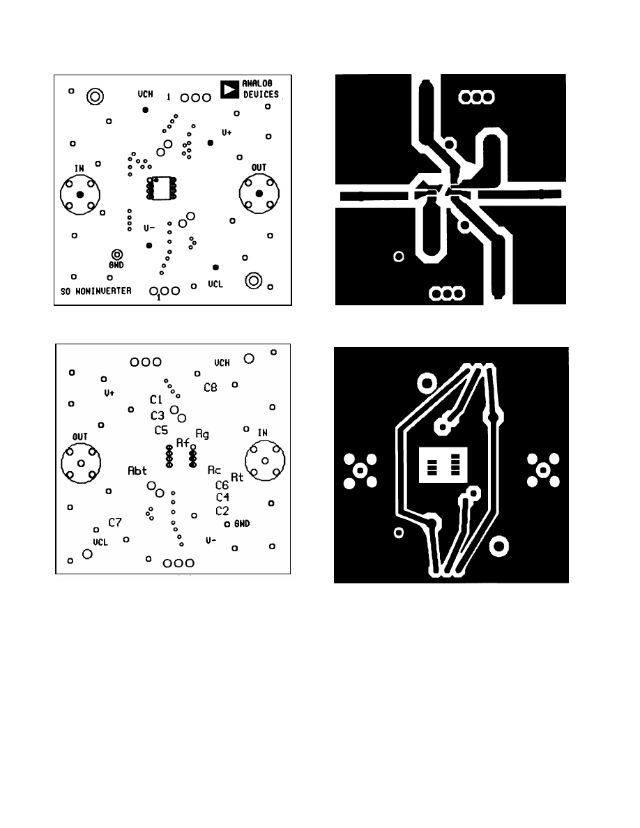
REV. 0
–22–
AD8036/AD8037
Figure 84. Evaluation Board Silkscreen (Top)
Figure 85. Evaluation Board Silkscreen (Bottom)
Figure 86. Board Layout (Solder Side)
Figure 87. Board Layout (Component Side)
AD8036/AD8037
REV. 0
–23–
OUTLINE DIMENSIONS
Dimensions shown in inches and (mm).
8-Pin Plastic DIP
(N Package)
8-Pin Plastic SOIC
(R Package)
8-Pin Cerdip
(Q Package)
0.320 (8.13)
0.290 (7.37)
0.015 (0.38)
0.008 (0.20)
15
°
0
°
0.005 (0.13) MIN
0.055 (1.4) MAX
1
PIN 1
4
5
8
0.310 (7.87)
0.220 (5.59)
0.405 (10.29) MAX
0.200
(5.08)
MAX
0.060 (1.52)
0.015 (0.38)
0.150
(3.81)
MIN
0.200 (5.08)
0.125 (3.18)
SEATING
PLANE
0.023 (0.58)
0.014 (0.36)
0.070 (1.78)
0.030 (0.76)
0.100
(2.54)
BSC
PIN 1
0.1574 (4.00)
0.1497 (3.80)
0.2440 (6.20)
0.2284 (5.80)
4
5
1
8
0.0098 (0.25)
0.0075 (0.19)
0.0500 (1.27)
0.0160 (0.41)
8
°
0
°
0.0196 (0.50)
0.0099 (0.25)
x 45
°
0.0500
(1.27)
BSC
0.0688 (1.75)
0.0532 (1.35)
0.0098 (0.25)
0.0040 (0.10)
0.1968 (5.00)
0.1890 (4.80)
0.0192 (0.49)
0.0138 (0.35)
PIN 1
0.280 (7.11)
0.240 (6.10)
4
5
8
1
0.060 (1.52)
0.015 (0.38)
0.130
(3.30)
MIN
0.210
(5.33)
MAX
0.160 (4.06)
0.115 (2.93)
0.430 (10.92)
0.348 (8.84)
SEATING
PLANE
0.022 (0.558)
0.014 (0.356)
0.070 (1.77)
0.045 (1.15)
0.100
(2.54)
BSC
0.325 (8.25)
0.300 (7.62)
0.015 (0.381)
0.008 (0.204)
0.195 (4.95)
0.115 (2.93)

REV. 0
–24–
AD8036/AD8037
PRINTED IN U.S.A.
C1980–10–10/94
Wyszukiwarka
Podobne podstrony:
8037
8037
8037
8037
(8037) konflikty i sposoby ich rozwiązywania, Zarządzanie, zarządzanie, Relacje pracownicze
8037
praca-magisterska-wa-c-8037, Dokumenty(2)
8037
8037
8037
więcej podobnych podstron