
DATA SHEET
Preliminary specification
File under Integrated Circuits, IC02
1996 Jul 18
INTEGRATED CIRCUITS
TDA4858
Economy Autosync Deflection
Controller (EASDC)

1996 Jul 18
2
Philips Semiconductors
Preliminary specification
Economy Autosync Deflection Controller
(EASDC)
TDA4858
FEATURES
Concept features
•
Full Horizontal (H) plus Vertical (V) autosync capability
•
Completely DC controllable for analog and digital
concepts
•
Excellent geometry control functions (e.g. automatic
correction of East-West (EW) parabola during
adjustment of vertical size and vertical shift)
•
Flexible Switched Mode Power Supply (SMPS) function
block for feedback and feed forward converters
•
X-ray protection
•
Start-up and switch-off sequence for safe operation of
all power components
•
Very good vertical linearity
•
Internal supply voltage stabilization
•
SDIP32 package.
Synchronization inputs
•
Can handle all sync signals (Horizontal, Vertical,
Composite and Sync-on-video)
•
Combined output for video clamping, vertical blanking
and protection blanking
•
Start of video clamping pulses externally selectable.
Horizontal section
•
Extremely low jitter
•
Frequency locked loop for smooth catching of line
frequency
•
Simple frequency preset of f
min
and f
max
by external
resistors
•
DC controllable wide range linear picture position
•
Soft start for horizontal driver.
Vertical section
•
Vertical amplitude independent of frequency
•
DC controllable picture height, picture position and
S-correction
•
Differential current outputs for DC coupling to vertical
booster.
EW section
•
Output for DC adjustable EW parabola
•
DC controllable picture width and trapezium correction
•
Optional tracking of EW parabola with line frequency
•
Prepared for additional DC controls of vertical linearity,
EW-corner, EW pin balance, EW parallelogram, vertical
focus by extended application.
GENERAL DESCRIPTION
The TDA4858 is a high performance and efficient solution
for autosync monitors. The concept is fully DC controllable
and can be used in applications with a microcontroller and
stand-alone in rock bottom solutions.
The TDA4858 provides synchronization processing, H + V
synchronization with full autosync capability, and very
short settling times after mode changes. External power
components are given a great deal of protection. The IC
generates the drive waveforms for DC-coupled vertical
boosters such as TDA486X and TDA8351.
The TDA4858 provides extended functions e.g. as a
flexible SMPS block and an extensive set of geometry
control facilities, providing excellent picture quality.
Together with the Philips TDA488X video processor family
a very advanced system solution is offered.
1996 Jul 18
3
Philips Semiconductors
Preliminary specification
Economy Autosync Deflection Controller
(EASDC)
TDA4858
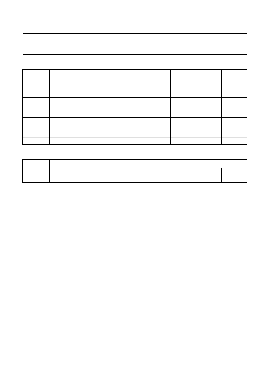
QUICK REFERENCE DATA
ORDERING INFORMATION
SYMBOL
PARAMETER
MIN.
TYP.
MAX.
UNIT
V
CC
supply voltage
9.2
−
16
V
I
CC
supply current
−
49
−
mA
∆
HPOS
horizontal shift adjustment range
−
±
10.5
−
%
∆
VAMP
vertical size adjustment range
60
−
100
%
∆
VPOS
vertical shift adjustment range
−
±
11.5
−
%
∆
VSCOR
vertical S-correction adjustment range
2
−
46
%
∆
V
EWPAR
EW parabola adjustment range
0.15
−
3.0
V
∆
V
EWWID
horizontal size adjustment range
0.2
−
4.0
V
∆
V
EWTRP
trapezium correction adjustment range
−
±
0.5
−
V
T
amb
operating ambient temperature
0
−
70
°
C
TYPE
NUMBER
PACKAGE
NAME
DESCRIPTION
VERSION
TDA4858
SDIP32
plastic shrink dual in-line package; 32 leads (400 mil)
SOT232-1
1996 Jul 18
4
Philips Semiconductors
Preliminary specification
Economy Autosync Deflection Controller
(EASDC)
TDA4858
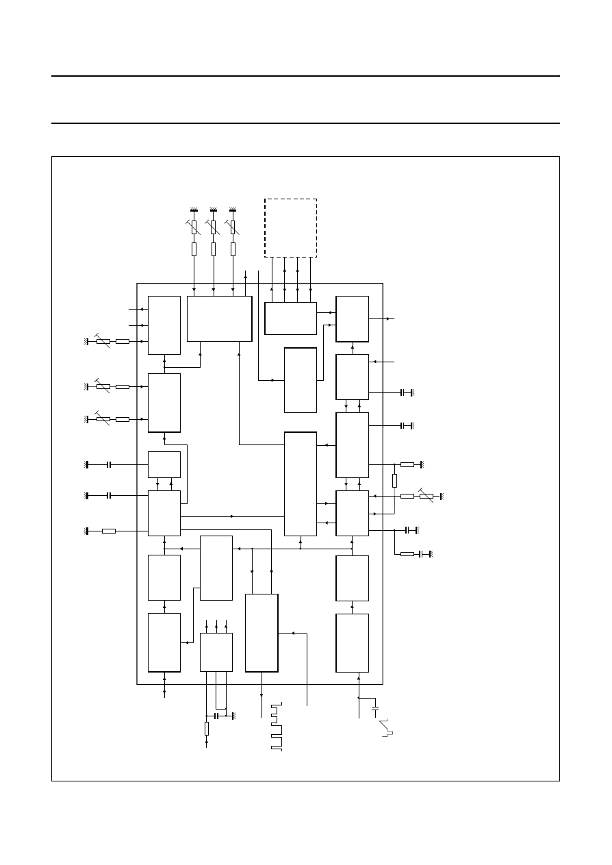
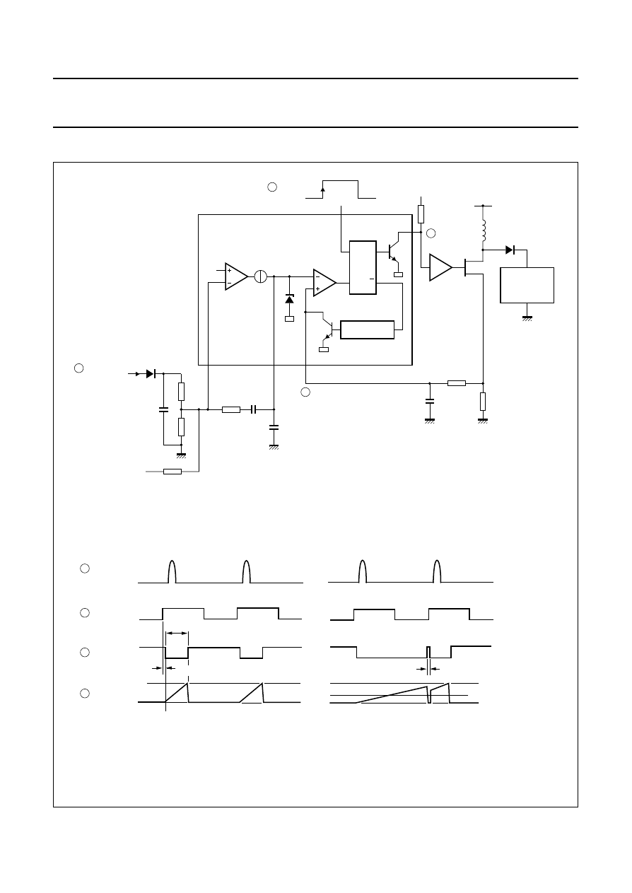
BLOCK DIAGRAM
handbook, full pagewidth
VERTICAL
SYNC
INPUT
POLARITY
CORRECTION
VERTICAL
OSCILLATOR
AGC
VERTICAL POSITION
VERTICAL SIZE
VERTICAL
OUTPUT STAGE
S-CORRECTION
SUPPLY
AND
REFERENCE
VERTICAL SYNC
INTEGRATOR
EW
PARABOLA
VIDEO CLAMPING PULSE
VERTICAL BLANKING
PLL1
PLL2
SYNC INPUT
POLARITY
CORRECTION
HORIZONTAL
OSCILLATOR
FREQUENCY DETECTOR
COINCIDENCE DETECTOR
X-RAY
PROTECTION
HORIZONTAL
OUTPUT
STAGE
B
+
CONTROL
B
+
CONTROL
APPLICATION
22
k
Ω
39 k
Ω
27 k
Ω
220
k
Ω
39
k
Ω
47 nF
1.5
nF
220 k
Ω
39 k
Ω
220 k
Ω
39 k
Ω
39 k
Ω
220 k
Ω
220 k
Ω
39 k
Ω
220 k
Ω
39 k
Ω
220 k
Ω
100
nF
VPOS
VAMP
VSCOR
100
nF
1%
5%
VCAP
VAGC
VREF
R
VREF
C
VCAP
C
VAGC
VOUT1
VOUT2
EW
parabola
horizontal
size
EWDRV
XRAY
BDRV
BSENS
BOP
BIN
EW
trapeziun
EWPAR
EWWID
EWTRP
HDRV
HFLB
12 nF
10 nF
HREF
HPLL2
2%
HCAP
R
HREF
R
HBUF
V
CC
(1)
(1)
(3)
(2)
HPLL1
HBUF
HPOS
HSYNC
(TTL level)
CLSEL
CLBL
VSYNC
(TTL level)
9.2 to 16 V
SGND
PGND
(video)
clamping
blanking
14
23
24
22
17
18
19
13
12
21
32
20
11
2
6
4
3
5
9
8
25
16
10
15
26
27
30
28
29
31
1
7
TDA4858
HORIZONTAL/
COMPOSITE
MGD094
Fig.1 Block diagram and application circuit.
(1)
See calculation of f
H
range.
(2)
See note
2 of Chapter
“Characteristics”.
(3)
See Figs
12
and
13.
1996 Jul 18
5
Philips Semiconductors
Preliminary specification
Economy Autosync Deflection Controller
(EASDC)
TDA4858
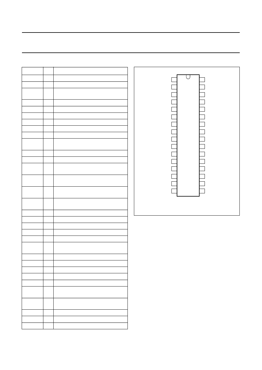
PINNING
SYMBOL PIN
DESCRIPTION
HFLB
1
horizontal flyback input
XRAY
2
X-ray protection input
BOP
3
B+ control OTA output;
comparator input
BSENS
4
B+ control comparator input/output
BIN
5
B+ control OTA input
BDRV
6
B+ control driver output
HDRV
7
horizontal driver output
PGND
8
power ground
V
CC
9
supply voltage
CLSEL
10
selection input for horizontal clamping
trigger
EWDRV
11
EW parabola output
VOUT2
12
vertical output 2 (ascending sawtooth)
VOUT1
13
vertical output 1 (descending
sawtooth)
VSYNC
14
vertical synchronization input/output
(TTL level)
HSYNC
15
horizontal/composite synchronization
input (TTL level or sync-on-video)
CLBL
16
video clamping pulse/vertical blanking
and protection output
VPOS
17
vertical shift input
VAMP
18
vertical size input
VSCOR
19
vertical S-correction input
EWTRP
20
EW trapezium correction input
EWPAR
21
EW parabola amplitude input
VAGC
22
external capacitor for vertical
amplitude control
VREF
23
external resistor for vertical oscillator
VCAP
24
external capacitor for vertical oscillator
SGND
25
signal ground
HPLL1
26
external filter for PLL1
HBUF
27
buffered f/v voltage output
HREF
28
reference current for horizontal
oscillator
HCAP
29
external capacitor for horizontal
oscillator
HPOS
30
horizontal shift input
HPLL2
31
external filter for PLL2/soft start
EWWID
32
horizontal size input
Fig.2 Pin configuration.
handbook, halfpage
TDA4858
MGD095
1
2
3
4
5
6
7
8
9
10
11
12
13
14
15
16
HFLB
XRAY
BOP
BSENS
BIN
BDRV
HDRV
PGND
VCC
CLSEL
EWDRV
VOUT2
VOUT1
VSYNC
HSYNC
CLBL
EWWID
HPLL2
HPOS
HCAP
HREF
HBUF
HPLL1
SGND
VCAP
VREF
VAGC
EWPAR
EWTRP
VSCOR
VAMP
VPOS
32
31
30
29
28
27
26
25
24
23
22
21
20
19
18
17

1996 Jul 18
6
Philips Semiconductors
Preliminary specification
Economy Autosync Deflection Controller
(EASDC)
TDA4858
FUNCTIONAL DESCRIPTION
Horizontal sync separator and polarity correction
HSYNC (pin 15) is the input for horizontal synchronization
signals, which can be DC-coupled TTL signals (horizontal
or composite sync) and AC-coupled negative-going video
sync signals. Video syncs are clamped to 1.28 V and
sliced at 1.4 V. This results in a fixed absolute slicing level
of 120 mV related to sync top.
For DC-coupled TTL signals the input clamping current is
limited. The slicing level for TTL signals is 1.4 V.
The separated sync signal (either video or TTL) is
integrated on an internal capacitor to detect and normalize
the sync polarity.
Normalized horizontal sync pulses are used as input
signals for the vertical sync integrator, the PLL1 phase
detector and the frequency-locked loop.
Vertical sync integrator
Normalized composite sync signals from HSYNC are
integrated on an internal capacitor in order to extract
vertical sync pulses. The integration time is dependent on
the horizontal oscillator reference current at HREF
(pin 28). The integrator output directly triggers the vertical
oscillator. This signal is available at VSYNC (normally
vertical sync input; pin 14), which is used as an output in
this mode.
Vertical sync slicer and polarity correction
Vertical sync signals (TTL) applied to VSYNC (pin 14) are
sliced at 1.4 V. The output signal of the sync slicer is
integrated on an internal capacitor to detect and normalize
the sync polarity.
If a composite sync signal is detected at HSYNC, VSYNC
is used as output for the integrated vertical sync (e.g. for
power saving applications).
Video clamping/vertical blanking generator
The video clamping/vertical blanking signal at CLBL
(pin 16) is a two-level sandcastle pulse which is especially
suitable for video ICs such as the TDA488X family, but
also for direct applications in video output stages.
The upper level is the video clamping pulse, which is
triggered by the trailing edge of the horizontal sync pulse.
The width of the video clamping pulse is determined by an
internal monoflop.
CLSEL (pin 10) is the selection input for the position of the
video clamping pulse. If CLSEL is connected to ground,
the clamping pulse is triggered with the trailing edge of
horizontal sync. For a clamping pulse which starts with the
leading edge of horizontal sync, pin 10 must be connected
to V
CC
.
The lower level of the sandcastle pulse is the vertical
blanking pulse, which is derived directly from the internal
oscillator waveform. It is started by the vertical sync and
stopped with the start of the vertical scan. This results in
optimum vertical blanking.
Blanking will be activated continuously, if one of the
following conditions is true:
No horizontal flyback pulses at HFLB (pin 1)
X-ray protection is activated
Soft start of horizontal drive (voltage at HPLL2 (pin 31)
is low)
Supply voltage at V
CC
(pin 9) is low (see Fig.14)
PLL1 is unlocked while frequency-locked loop is in
search mode.
Blanking will not be activated if the horizontal sync
frequency is below the valid range or there are no sync
pulses available.

1996 Jul 18
7
Philips Semiconductors
Preliminary specification
Economy Autosync Deflection Controller
(EASDC)
TDA4858
Frequency-locked loop
The frequency-locked loop can lock the horizontal
oscillator over a wide frequency range. This is achieved by
a combined search and PLL operation. The frequency
range is preset by two external resistors and the
recommended ratio is
Larger ranges are possible by extended applications.
Without a horizontal sync signal the oscillator will be
free-running at f
min
. Any change of sync conditions is
detected by the internal coincidence detector. A deviation
of more than 4% between horizontal sync and oscillator
frequency switches the horizontal section into search
mode. This means that PLL1 control currents are switched
off immediately. Then the internal frequency detector
starts tuning the oscillator. Very small DC currents at
HPLL1 (pin 26) are used to perform this tuning with a well
defined change rate. When coincidence between
horizontal sync and oscillator frequency is detected, the
search mode is replaced by a normal PLL operation.
This operation ensures a smooth tuning and avoids fast
changes of horizontal frequency during catching.
In this concept it is not allowed to load HPLL1.
The frequency dependent voltage at this pin is fed
internally to HBUF (pin 27) via a sample-and-hold and
buffer stage. The sample-and-hold stage removes all
disturbances caused by horizontal sync or composite
vertical sync from the buffered voltage. An external
resistor from HBUF to HREF defines the frequency range.
See also hints for locking procedure in note 2 of
Chapter “Characteristics”.
PLL1 phase detector
The phase detector is a standard type using switched
current sources. It compares the middle of horizontal sync
with a fixed point on the oscillator sawtooth voltage.
The PLL1 loop filter is connected to HPLL1 (pin 26).
Horizontal oscillator
The horizontal oscillator is of the relaxation type and
requires a capacitor of 10 nF at HCAP (pin 29).
For optimum jitter performance the value of 10 nF must not
be changed.
The maximum oscillator frequency is determined by a
resistor from HREF to ground. A resistor from HREF to
HBUF defines the frequency range.
f
min
f
max
-----------
1
3.5
--------
=
The reference current at HREF also defines the integration
time constant of the vertical sync integration.
Calculation of line frequency range
First the oscillator frequencies f
min
and f
max
have to be
calculated. This is achieved by adding the spread of the
relevant components to the highest and lowest sync
frequencies f
S(min)
and f
S(max)
. The oscillator is driven by
the difference of the currents in R
HREF
and R
HBUF
. At the
highest oscillator frequency R
HBUF
does not contribute to
the spread. The spread will increase towards lower
frequencies due to the contribution of R
HBUF
. It is also
dependent on the ratio
The following example is a 31.45 to 64 kHz application:
Table 1
Calculation of total spread
Thus the typical frequency range of the oscillator in this
example is:
The resistors R
HREF
and R
HBUF
can be calculated with the
following formulae:
Where:
spread of:
for f
max
for f
min
IC
3%
3%
C
HCAP
2%
2%
R
HREF
1%
−
R
HREF
, R
HBUF
−
1%
×
(2.3
×
n
S
−
1)
Total
6%
8.69%
n
S
f
S max
(
)
f
S min
(
)
-------------------
=
n
S
f
S max
(
)
f
S min
(
)
-------------------
64 kHz
31.45 kHz
---------------------------
2.04
=
=
=
f
max
f
S max
(
)
1.06
×
67.84 kHz
=
=
f
min
f
S min
(
)
1.087
------------------
28.93 kHz
=
=
R
HREF
74
kHz
k
×
×
Ω
f
max
kHz
[
]
--------------------------------------
1.091 k
Ω
=
=
R
HBUF
R
HREF
1.19
×
n
×
n
1
–
---------------------------------------------
2.26 k
Ω
=
=
n
f
max
f
min
-----------
2.35
=
=

1996 Jul 18
8
Philips Semiconductors
Preliminary specification
Economy Autosync Deflection Controller
(EASDC)
TDA4858
The spread of f
min
increases with the frequency
ratio
.
For higher ratios this spread can be reduced by using
resistors with less tolerances.
PLL2 phase detector
The PLL2 phase detector is similar to the PLL1 detector
and compares the line flyback pulse at HFLB (pin 1) with
the oscillator sawtooth voltage. The PLL2 detector thus
compensates for the delay in the external horizontal
deflection circuit by adjusting the phase of the HDRV
(pin 7) output pulse.
The phase between horizontal flyback and horizontal sync
can be controlled at HPOS (pin 30).
If HPLL2 is pulled to ground, horizontal output pulses,
vertical output currents and B+ control driver pulses are
inhibited. This means, HDRV (pin 7), BDRV (pin 6)
VOUT1 (pin 13) and VOUT2 (pin 12) are floating in this
state. PLL2 and the frequency-locked loop are disabled,
and CLBL (pin 16) provides a continuous blanking signal.
This option can be used for soft start, protection and
power-down modes. When the HPLL2 voltage is released
again, an automatic soft start sequence will be performed
(see Fig.15).
The soft start timing is determined by the filter capacitor at
HPLL2 (pin 31), which is charged with an constant current
during soft start. In the beginning the horizontal driver
stage generates very small output pulses. The width of
these pulses increases with the voltage at HPLL2 until the
final duty factor is reached. At this point BDRV (pin 6),
VOUT1 (pin 13) and VOUT2 (pin 12) are re-enabled.
The voltage at HPLL2 continues to rise until PLL2 enters
its normal operating range. The internal charge current is
now disabled. Finally PLL2 and the frequency-locked loop
are enabled, and the continuous blanking at CLBL is
removed.
Horizontal phase adjustment
HPOS (pin 30) provides a linear adjustment of the relative
phase between the horizontal sync and oscillator
sawtooth. Once adjusted, the relative phase remains
constant over the whole frequency range.
Application hint: HPOS is a current input, which provides
an internal reference voltage while I
HPOS
is in the specified
adjustment current range. By grounding HPOS the
symmetrical control range is forced to its centre value,
f
S max
(
)
f
S min
(
)
-------------------
therefore the phase between horizontal sync and
horizontal drive pulse is only determined by PLL2.
Output stage for line drive pulses
An open collector output stage allows direct drive of an
inverting driver transistor because of a low saturation
voltage of 0.3 V at 20 mA. To protect the line deflection
transistor, the output stage is disabled (floating) for low
supply voltage at V
CC
(see Fig.14).
The duty factor of line drive pulses is slightly dependent on
the actual line frequency. This ensures optimum drive
conditions over the whole frequency range.
X-ray protection
The X-ray protection input XRAY (pin 2) provides a voltage
detector with a precise threshold. If the input voltage at
XRAY exceeds this threshold for a certain time, an internal
latch switches the IC into protection mode. In this mode
several pins are forced into defined states:
Horizontal output stage (HDRV) is floating
B+ control driver stage (BDRV) is floating
Vertical output stages (VOUT1 and VOUT2) are floating
CLBL provides a continuous blanking signal
The capacitor connected to HPLL2 (pin 31) is
discharged.
To reset the latch and return to normal operation, V
CC
has
to be temporarily switched off.
Vertical oscillator and amplitude control
This stage is designed for fast stabilization of vertical
amplitude after changes in sync frequency conditions.
The free-running frequency f
osc(V)
is determined by the
resistor R
VREF
connected to pin 23 and the capacitor
C
VCAP
connected to pin 24. The value of R
VREF
is not only
optimized for noise and linearity performance in the whole
vertical and EW section, but also influences several
internal references. Therefore the value of R
VREF
must not
be changed. Capacitor C
VCAP
should be used to select the
free-running frequency of the vertical oscillator in
accordance with the following formula:
f
osc V
( )
1
10.8
R
VREF
×
C
VCAP
×
-----------------------------------------------------------
=

1996 Jul 18
9
Philips Semiconductors
Preliminary specification
Economy Autosync Deflection Controller
(EASDC)
TDA4858
To achieve a stabilized amplitude the free-running
frequency f
osc(V)
, without adjustment, should be at least
10% lower than the minimum trigger frequency.
The contributions shown in Table 2 can be assumed.
Table 2
Calculation of f
osc(V)
total spread
Result for 50 to 110 Hz application:
Application hint: VAGC (pin 22) has a high input
impedance during scan, thus the pin must not be loaded
externally. Otherwise non-linearities in the vertical output
currents may occur due to the changing charge current
during scan.
Application hint: The full vertical sync range of 1 : 2.5 can
be made usable by incorporating an adjustment of the
free-running frequency. Also the complete sync range can
be shifted to higher frequencies (e.g. 70 to 160 Hz) by
reducing the value of C
VCAP
.
Adjustment of vertical size, vertical shift and
S-correction
VPOS (pin 17) is the input for the DC adjustable vertical
picture shift. This pin provides a phase shift at the
sawtooth output VOUT1 and VOUT2 (pins 13 and 12) and
the EW drive output EWDRV (pin 11) in such a way, that
the whole picture moves vertically while maintaining the
correct geometry.
The amplitude of the differential output currents at VOUT1
and VOUT2 can be adjusted via input VAMP (pin 18).
This can be a combination of a DC adjustment and a
dynamic waveform modulation.
VSCOR (pin 19) is used to adjust the amount of vertical
S-correction in the output signal.
The adjustments for vertical size and vertical shift also
affect the waveforms of the EW parabola and the vertical
S-correction. The result of this interaction is that no
Contributing elements:
Minimum frequency offset between f
osc(V)
and lowest trigger frequency
±
10%
Spread of IC
±
3%
Spread of R
VREF
±
1%
Spread of C
VCAP
±
5%
Total
19%
f
osc V
( )
50 Hz
1.19
---------------
42 Hz
=
=
readjustment of these parameters is necessary after an
adjustment of vertical picture size or position.
Application hint: VPOS is a current input, which provides
an internal reference voltage while I
VPOS
is in the specified
adjustment current range. By grounding VPOS (pin 17) the
symmetrical control range is forced to its centre value.
Application hint: VSCOR is a current input at 5 V.
Superimposed on this level is a very small positive-going
vertical sawtooth, intended to modulate an external
long-tailed transistor pair. This enables further optional DC
controls of functions which are not directly accessible such
as vertical tilt or vertical linearity (see Fig.17).
EW parabola (including horizontal size and trapezium
correction)
EWDRV (pin 11) provides a complete EW drive waveform.
EW parabola amplitude, DC shift (horizontal size) and
trapezium correction can be controlled via separate DC
inputs.
EWPAR (pin 21) is used to adjust the parabola amplitude.
This can be a combination of a DC adjustment and a
dynamic waveform modulation.
The EW parabola amplitude also tracks with vertical
picture size. The parabola waveform itself tracks with the
adjustment for vertical picture shift (VPOS).
EWWID (pin 32) offers two modes of operation:
1. Mode 1
Horizontal size is DC controlled via EWWID (pin 32)
and causes a DC shift at the EWDRV output. Also the
complete waveform is multiplied internally by a signal
proportional to the line frequency (which is detected
via the current at HREF (pin 28). This mode is to be
used for driving EW modulator stages which require a
voltage proportional to the line frequency.
2. Mode 2
EWWID (pin 32) is grounded. Then EWDRV is no
longer multiplied by the line frequency. The DC
adjustment for horizontal size must be added to the
input of the B+ control amplifier BIN (pin 5). This mode
is to be used for driving EW modulators which require
a voltage independent of the line frequency.
EWTRP (pin 20) is used to adjust the amount of trapezium
correction in the EW drive waveform.

1996 Jul 18
10
Philips Semiconductors
Preliminary specification
Economy Autosync Deflection Controller
(EASDC)
TDA4858
Application hint: EWTRP (pin 20) is a current input at
5 V. Superimposed on this level is a very small vertical
parabola with positive tips, intended to modulate an
external long-tailed transistor pair. This enables further
optional DC controls of functions which are not directly
accessible such as EW-corner, vertical focus or EW pin
balance (see Fig.17).
Application hint: By grounding EWTRP (pin 20) the
symmetrical control range is forced to its centre value.
B+ control function block
The B+ control function block of the EASDC consists of an
Operational Transconductance Amplifier (OTA), a voltage
comparator, a flip-flop and a discharge circuit.
This configuration allows easy applications for different
B+ control concepts.
G
ENERAL DESCRIPTION
The non-inverting input of the OTA is connected internally
to a high precision reference voltage. The inverting input is
connected to BIN (pin 5). An internal clamping circuit limits
the maximum positive output voltage of the OTA.
The output itself is connected to BOP (pin 3) and to the
inverting input of the voltage comparator.
The non-inverting input of the voltage comparator can be
accessed via BSENS (pin 4).
B+ drive pulses are generated by an internal flip-flop and
fed to BDRV (pin 6) via an open collector output stage.
This flip-flop will be set at the rising edge of the signal at
HDRV (pin 7). The falling edge of the output signal at
BDRV has a defined delay of t
d(BDRV)
to the rising edge of
the HDRV pulse. When the voltage at BSENS exceeds the
voltage at BOP, the voltage comparator output resets the
flip-flop, and therefore the open collector stage at BDRV is
floating again.
An internal discharge circuit allows a well defined
discharge of capacitors at BSENS. BDRV is active at a low
level output voltage (see Figs 12 and 13), thus it requires
an external inverting driver stage.
The B+ function block can be used for B+ deflection
modulators in either of two modes:
•
Feedback mode (see Fig.12)
In this application the OTA is used as an error amplifier
with a limited output voltage range. The flip-flop will be
set at the rising edge of the signal at HDRV. A reset will
be generated when the voltage at BSENS taken from
the current sense resistor exceeds the voltage at BOP.
If no reset is generated within a line period, the rising
edge of the next HDRV pulse forces the flip-flop to reset.
The flip-flop is set immediately after the voltage at
BSENS has dropped below the threshold voltage
V
RESTART(BSENS)
.
•
Feed forward mode (see Fig.13)
This application uses an external RC combination at
BSENS to provide a pulse width which is independent
from the horizontal frequency. The capacitor is charged
via an external resistor and discharged by the internal
discharge circuit. For normal operation the discharge
circuit is activated when the flip-flop is reset by the
internal voltage comparator. Now the capacitor will be
discharged with a constant current until the internally
controlled stop level V
STOP(BSENS)
is reached. This level
will be maintained until the rising edge of the next HDRV
pulse sets the flip-flop again and disables the discharge
circuit.
If no reset is generated within a line period, the rising
edge of the next HDRV pulse automatically starts the
discharge sequence and resets the flip-flop (Fig.13).
When the voltage at BSENS reaches the threshold
voltage V
RESTART(BSENS)
, the discharge circuit will be
disabled automatically and the flip-flop will be set
immediately. This behaviour allows a definition of the
maximum duty cycle of the B+ control drive pulse by the
relationship of charge current to discharge current.

1996 Jul 18
11
Philips Semiconductors
Preliminary specification
Economy Autosync Deflection Controller
(EASDC)
TDA4858
Supply voltage stabilizer, references and protection
The ASDC provides an internal supply voltage stabilizer
for excellent stabilization of all internal references.
An internal gap reference especially designed for
low-noise is the reference for the internal horizontal and
vertical supply voltages. All internal reference currents and
drive current for the vertical output stage are derived from
this voltage via external resistors.
A special protection mode has been implemented in order
to protect the deflection stages and the picture tube during
start-up, shut-down and fault conditions. This protection
mode can be activated as shown in Table 3.
Table 3
Activation of protection mode
When protection mode is active, several pins of the ASDC
are forced into a defined state:
HDRV (horizontal driver output) is floating
BDRV (B+ control driver output) is floating
VOUT1 and VOUT2 (vertical outputs) are floating
CLBL provides a continuous blanking signal
The capacitor at HPLL2 is discharged.
If the protection mode is activated via the supply voltage at
pin 9, all these actions will be performed in a well defined
sequence (see Fig.14). For activation via X-ray protection
or HPLL2 all actions will occur simultaneously.
ACTIVATION
RESET
Low supply voltage at pin 9
increase supply voltage
X-ray protection XRAY (pin 2)
triggered
remove supply voltage
HPLL2 (pin 31) pulled to
ground
release pin 31
The return to normal operation is performed in accordance
with the start-up sequence in Fig.14a, if the reset was
caused by the supply voltage at pin 9. The first action with
increasing supply voltage is the activation of continuous
blanking at CLBL. When the threshold for activation of
HDRV is passed, an internal current begins to charge the
external capacitor at HPLL2 and a PLL2 soft start
sequence is performed (see Fig.15). In the beginning of
this phase the horizontal driver stage generates very small
output pulses. The width of these pulses increases with the
voltage at HPLL2 until the final duty cycle is reached.
Then the PLL2 voltage passes the threshold for activation
of BDRV, VOUT1 and VOUT2.
For activation of these pins not only the PLL2 voltage, but
also the supply voltage must have passed the appropriate
threshold. A last pair of thresholds has to be passed by
PLL2 voltage and supply voltage before the continuous
blanking is finally removed, and the operation of PLL2 and
frequency-locked loop is enabled.
A return to the normal operation by releasing the voltage
at HPLL2 will lead to a slightly different sequence. Here the
activation of all functions is influenced only by the voltage
at HPLL2 (see Fig.15).
Application hint: Internal discharge of the capacitor at
HPLL2 will only be performed, if the protection mode was
activated via the supply voltage or X-ray protection.

1996 Jul 18
12
Philips Semiconductors
Preliminary specification
Economy Autosync Deflection Controller
(EASDC)
TDA4858
LIMITING VALUES
In accordance with the Absolute Maximum Rating System (IEC 134); all voltages measured with respect to ground.
Note
1. Machine model: 200 pF, 25
Ω
, 2.5
µ
H; human body model: 100 pF, 1500
Ω
, 7.5
µ
H.
THERMAL CHARACTERISTICS
QUALITY SPECIFICATION
In accordance with
“URF-4-2-59/601”; EMC emission/immunity test in accordance with “DIS 1000 4.6” (IEC 801.6)
Note
1. Tests are performed with application reference board. Tests with other boards will have different results.
SYMBOL
PARAMETER
MIN.
MAX.
UNIT
V
CC
supply voltage
−
0.5
+16
V
V
I(n)
input voltages
BIN
−
0.5
+6.0
V
HSYNC, VPOS, VAMP, VSCOR, VREF, HREF and HPOS
−
0.5
+6.5
V
XRAY
−
0.5
+8.0
V
CLSEL
−
0.5
+16
V
V
O(n)
output voltages
VOUT1 and VOUT2
−
0.5
+6.5
V
BDRV and HDRV
−
0.5
+16
V
V
I/O(n)
input/output voltages
BOP and BSENS
−
0.5
+6.0
V
VSYNC
−
0.5
+6.5
V
I
HDRV
horizontal driver output current
−
100
mA
I
HFLB
horizontal flyback input current
−
10
+10
mA
I
CLBL
video clamping pulse/vertical blanking output current
−
−
10
mA
I
BOP
B+ control OTA output current
−
1
mA
I
BDRV
B+ control driver output current
−
50
mA
I
EWDRV
EW driver output current
−
−
5
mA
T
amb
operating ambient temperature
0
70
°
C
T
j
junction temperature
−
150
°
C
T
stg
storage temperature
−
55
+150
°
C
V
esd
electrostatic discharge for all pins (note 1)
machine model
−
400
+400
V
human body model
−
3000
+3000
V
SYMBOL
PARAMETER
VALUE
UNIT
R
th j-a
thermal resistance from junction to ambient in free air
55
K/W
SYMBOL
PARAMETER
CONDITIONS
MIN.
TYP.
MAX.
UNIT
V
EMC
emission test
note 1
−
1.5
−
mV
immunity test
note 1
−
2.0
−
V

1996 Jul 18
13
Philips Semiconductors
Preliminary specification
Economy Autosync Deflection Controller
(EASDC)
TDA4858
CHARACTERISTICS
V
CC
= 12 V; T
amb
= 25
°
C; peripheral components in accordance with Fig.1; unless otherwise specified.
SYMBOL
PARAMETER
CONDITIONS
MIN.
TYP.
MAX.
UNIT
Horizontal sync separator
I
NPUT CHARACTERISTICS FOR DC
-
COUPLED
TTL
SIGNALS
[HSYNC (
PIN
15)]
V
DC(HSYNC)
sync input signal voltage
1.7
−
−
V
slicing voltage level
1.2
1.4
1.6
V
t
r(HSYNC)
rise time of sync pulse
10
−
500
ns
t
f(HSYNC)
fall time of sync pulse
10
−
500
ns
t
W(HSYNC)
minimum width of sync pulse
0.7
−
−
µ
s
I
DC(HSYNC)
input current
V
HSYNC
= 0.8 V
−
−
−
200
µ
A
V
HSYNC
= 5.5 V
−
−
10
µ
A
I
NPUT CHARACTERISTICS FOR
AC-
COUPLED VIDEO SIGNALS
(
SYNC
-
ON
-
VIDEO
,
NEGATIVE SYNC POLARITY
)
V
AC(HSYNC)
sync amplitude of video input
signal voltage
−
300
−
mV
slicing voltage level
(measured from top sync)
source resistance
R
S
= 50
Ω
90
120
150
mV
V
clamp(HSYNC)
top sync clamping voltage level
1.1
1.28
1.5
V
I
C(HSYNC)
charge current for coupling
capacitor
V
HSYNC
>
V
clamp(HSYNC)
1.7
2.4
3.4
µ
A
t
HSYNC(min)
minimum width of sync pulse
0.7
−
−
µ
s
R
S(max)
maximum source resistance
duty factor = 7%
−
−
1500
Ω
r
diff(HSYNC)
differential input resistance
during sync
−
80
−
Ω
Automatic polarity correction for horizontal sync
horizontal sync pulse width
related to t
H
f
H
<
45 kHz
−
−
20
%
f
H
>
45 kHz
−
−
25
%
t
P(H)
delay time for changing polarity
0.3
−
1.8
ms
Vertical sync integrator
t
int(V)
integration time for generation
of a vertical trigger pulse
f
H
= 31.45 kHz;
I
HREF
= 1.052 mA
7
10
13
µ
s
f
H
= 64 kHz;
I
HREF
= 2.141 mA
3.9
5.7
6.5
µ
s
f
H
= 100 kHz;
I
HREF
= 3.345 mA
2.5
3.8
4.5
µ
s
Vertical sync slicer (DC-coupled, TTL compatible) [VSYNC (pin 14)]
V
VSYNC
sync input signal voltage
1.7
−
−
V
slicing voltage level
1.2
1.4
1.6
V
I
VSYNC
input current
0 V
<
V
SYNC
<
5.5 V
−
−
±
10
µ
A
t
P H
( )
t
H
-------------

1996 Jul 18
14
Philips Semiconductors
Preliminary specification
Economy Autosync Deflection Controller
(EASDC)
TDA4858
V
ERTICAL SYNC OUTPUT AT
VSYNC (
PIN
14)
DURING COMPOSITE SYNC AT
HSYNC (
PIN
15)
I
VSYNC
output current
during internal vertical
sync
−
0.7
−
1.0
−
1.35
mA
V
VSYNC
internal clamping voltage level
during internal vertical
sync
4.4
4.8
5.2
V
steepness of slopes
−
300
−
ns/mA
Automatic polarity correction for vertical sync
t
VSYNC(max)
maximum width of vertical sync
pulse
−
−
300
µ
s
t
d(VPOL)
delay for changing polarity
0.3
−
1.8
ms
Video clamping/vertical blanking output [CLBL (pin 16)]
t
clamp(CLBL)
width of video clamping pulse
measured at V
CLBL
= 3 V
0.6
0.7
0.8
µ
s
V
clamp(CLBL)
top voltage level of video
clamping pulse
4.32
4.75
5.23
V
TC
clamp
temperature coefficient of
V
clamp(CLBL)
−
+4
−
mV/K
steepness of slopes for
clamping pulse
R
L
= 1 M
Ω
; C
L
= 20 pF
−
50
−
ns/V
V
blank(CLBL)
top voltage level of vertical
blanking pulse
note 1
1.7
1.9
2.1
V
t
blank(CLBL)
width of vertical blanking pulse
240
300
360
µ
s
TC
blank
temperature coefficient of
V
blank(CLBL)
−
+2
−
mV/K
V
scan(CLBL)
output voltage during vertical
scan
I
CLBL
= 0
0.59
0.63
0.67
V
TC
scan
temperature coefficient of
V
scan(CLBL)
−
−
2
−
mV/K
I
sink(CLBL)
internal sink current
2.4
−
−
mA
I
load(CLBL)
external load current
−
−
−
3.0
mA
SYMBOL
PARAMETER
CONDITIONS
MIN.
TYP.
MAX.
UNIT

1996 Jul 18
15
Philips Semiconductors
Preliminary specification
Economy Autosync Deflection Controller
(EASDC)
TDA4858
S
ELECTION OF LEADING
/
TRAILING EDGE TRIGGER FOR VIDEO CLAMPING PULSE
V
CLSEL
voltage at CLSEL (pin 10) for
trigger with leading edge of
horizontal sync
7
−
V
CC
V
voltage at CLSEL for trigger
with trailing edge of horizontal
sync
0
−
5
V
t
d(clamp)
delay between leading edge of
horizontal sync and start of
horizontal clamping pulse
V
CLSEL
> 7 V
−
300
−
ns
delay between trailing edge of
horizontal sync and start of
horizontal clamping pulse
V
CLSEL
< 5 V
−
130
−
ns
t
clamp(max)
maximum duration of video
clamping pulse after end of
horizontal sync
V
CLBL
= 3 V; V
CLSEL
> 7 V
−
−
0.15
µ
s
V
CLBL
= 3 V; V
CLSEL
< 5 V
−
−
1.0
µ
s
R
CLSEL
input resistance at CLSEL
(pin 10)
V
CLSEL
≤
V
CC
80
−
−
k
Ω
PLL1 phase comparator and frequency-locked loop [HPLL1 (pin 26) and HBUF (pin 27)]
t
HSYNC(max)
maximum width of horizontal
sync pulse (referenced to line
period)
f
H
<
45 kHz; note 2
−
−
20
%
f
H
>
45 kHz; note 2
−
−
25
%
t
lock(HPLL1)
total lock-in time of PLL1
−
40
80
ms
V
HPLL1
control voltage
notes 3 and 4
V
HBUF
buffered f/v voltage at HBUF
(pin 27)
f
H(min)
; note 5
−
5.6
−
V
f
H(max)
; note 5
−
2.5
−
V
I
load(HBUF)
maximum load current
−
−
−
4.0
mA
A
DJUSTMENT OF HORIZONTAL PICTURE POSITION
∆
HPOS
horizontal shift adjustment
range (referenced to horizontal
period)
I
HSHIFT
= 0
−
−
10.5
−
%
I
HSHIFT
=
−
135
µ
A
−
+10.5
−
%
I
HPOS
input current
∆
HPOS = +10.5%
−
110
−
120
−
135
µ
A
∆
HPOS =
−
10.5%
−
0
−
µ
A
V
ref(HPOS)
reference voltage at input
note 6
−
5.1
−
V
V
off(HPOS)
picture shift is centred if HPOS
(pin 30) is forced to ground
0
−
0.1
V
SYMBOL
PARAMETER
CONDITIONS
MIN.
TYP.
MAX.
UNIT

1996 Jul 18
16
Philips Semiconductors
Preliminary specification
Economy Autosync Deflection Controller
(EASDC)
TDA4858
Horizontal oscillator [HCAP (pin 29) and HREF (pin 28)]
f
H(0)
free-running frequency without
PLL1 action (for testing only)
R
HBUF
=
∞
;
R
HREF
= 2.4 k
Ω
;
C
HCAP
= 10 nF; note 4
30.53
31.45
32.39
kHz
∆
f
H(0)
spread of free-running
frequency (excluding spread of
external components)
−
−
±
3.0
%
TC
temperature coefficient of
free-running frequency
−
100
0
+100
10
−
6
/K
f
H(max)
maximum oscillator frequency
−
−
130
kHz
V
HREF
voltage at input for reference
current
2.43
2.55
2.68
V
PLL2 phase detector [HFLB (pin 1) and HPLL2 (pin 31)]
∆φ
PLL2
PLL2 control (advance of
horizontal drive with respect to
middle of horizontal flyback)
maximum advance
36
−
−
%
minimum advance
−
7
−
%
t
d(HFLB)
delay between middle of
horizontal sync and middle of
horizontal flyback
HPOS (pin 30) grounded
−
200
−
ns
V
PROT(HPLL2)
maximum voltage for PLL2
protection mode/soft start
−
4.4
−
V
I
charge(HPLL2)
charge current for external
capacitor during soft start
V
HPLL2
<
3.7 V
−
15
−
µ
A
H
ORIZONTAL FLYBACK INPUT
[HFLB (
PIN
1)]
V
HFLB
positive clamping level
I
HFLB
= 5 mA
−
5.5
−
V
negative clamping level
I
HFLB
=
−
1 mA
−
−
0.75
−
V
I
HFLB
positive clamping current
−
−
6
mA
negative clamping current
−
−
−
2
mA
V
HFLB
slicing level
−
2.8
−
V
Output stage for line driver pulses [HDRV (pin 7)]
O
PEN COLLECTOR OUTPUT STAGE
V
HDRV
saturation voltage
I
HDRV
= 20 mA
−
−
0.3
V
I
HDRV
= 60 mA
−
−
0.8
V
I
leakage(HDRV)
output leakage current
V
HDRV
= 16 V
−
−
10
µ
A
A
UTOMATIC VARIATION OF DUTY FACTOR
t
HDRV(OFF)
/t
H
relative t
OFF
time of HDRV
output; measured at
V
HDRV
= 3 V; HDRV duty factor
is determined by the relation
I
HREF
/I
VREF
I
HDRV
= 20 mA;
f
H
= 31.45 kHz; see Fig.9
42
45
48
%
I
HDRV
= 20 mA;
f
H
= 57 kHz; see Fig.9
45
46.3
47.7
%
I
HDRV
= 20 mA;
f
H
= 90 kHz; see Fig.9
46.6
48
49.4
%
SYMBOL
PARAMETER
CONDITIONS
MIN.
TYP.
MAX.
UNIT

1996 Jul 18
17
Philips Semiconductors
Preliminary specification
Economy Autosync Deflection Controller
(EASDC)
TDA4858
X-ray protection [XRAY (pin 2)]
V
XRAY
slicing voltage level
6.14
6.38
6.64
V
t
W(XRAY)
minimum width of trigger pulse
10
−
−
µ
s
R
I(XRAY)
input resistance at XRAY
(pin 2)
V
XRAY
<
6.38 V + V
BE
500
−
−
k
Ω
V
XRAY
>
6.38 V + V
BE
−
5
−
k
Ω
V
RESET(VCC)
supply voltage for reset of
X-ray latch
−
5.6
−
V
Vertical oscillator (oscillator frequency in application without adjustment of free-running frequency f
v(o)
)
f
V
free-running frequency
R
VREF
= 22 k
Ω
;
C
VCAP
= 100 nF
40
42
43.3
Hz
f
v(o)
vertical frequency catching
range
constant amplitude;
notes 7, 8 and 9
50
−
110
Hz
V
VREF
voltage at reference input for
vertical oscillator
−
3.0
−
V
t
d(scan)
delay between trigger pulse
and start of ramp at VCAP
(pin 24) (width of vertical
blanking pulse)
240
300
360
µ
s
I
VAGC
control currents of amplitude
control
±
120
±
200
±
300
µ
A
C
VAGC
external capacitor at VAGC
(pin 22)
−
−
150
nF
Differential vertical current outputs
A
DJUSTMENT OF VERTICAL SIZE
(see Figs 3 to 8) [VAMP (
PIN
18)]
∆
VAMP
vertical size adjustment range
(referenced to nominal vertical
size)
I
VAMP
= 0; note 10
−
60
−
%
I
VAMP
=
−
135
µ
A; note 10
−
100
−
%
I
VAMP
input current for maximum
amplitude (100%)
−
110
−
120
−
135
µ
A
input current for minimum
amplitude (60%)
−
0
−
µ
A
V
ref(VAMP)
reference voltage at input
−
5.0
−
V
A
DJUSTMENT OF VERTICAL SHIFT
(see Figs 3 to 8) [VPOS (
PIN
17)]
∆
VPOS
vertical shift adjustment range
(referenced to 100% vertical
size)
I
VPOS
=
−
135
µ
A; note 10
−
−
11.5
−
%
I
VPOS
= 0; note 10
−
+11.5
−
%
I
VPOS
input current for maximum
shift-up
−
110
−
120
−
135
µ
A
input current for maximum
shift-down
−
0
−
µ
A
V
ref(VPOS)
reference voltage at input
−
5.0
−
V
V
off(VPOS)
vertical shift is centred if VPOS
(pin 17) is forced to ground
0
−
0.1
V
SYMBOL
PARAMETER
CONDITIONS
MIN.
TYP.
MAX.
UNIT

1996 Jul 18
18
Philips Semiconductors
Preliminary specification
Economy Autosync Deflection Controller
(EASDC)
TDA4858
A
DJUSTMENT OF VERTICAL S
-
CORRECTION
(see Figs 3 to 8) [VSCOR (
PIN
19)]
∆
VSCOR
vertical S-correction
adjustment range
I
VSCOR
= 0; note 10
−
2
−
%
I
VSCOR
=
−
135
µ
A;
note 10
−
46
−
%
I
VSCOR
input current for maximum
S-correction
−
110
−
120
−
135
µ
A
input current for minimum
S-correction
−
0
−
µ
A
δ
VSCOR
symmetry error of S-correction
maximum
∆
VSCOR
−
−
±
0.7
%
V
ref(VSCOR)
reference voltage at input
−
5.0
−
V
V
SAWM(p-p)
voltage amplitude of
superimposed logarithmic
sawtooth (peak-to-peak value)
note 11
−
−
145
mV
Vertical output stage [VOUT1 (pin 13) and VOUT2 (pin 12)]
∆
I
VOUT(nom)
nominal differential output
current (peak-to-peak value)
(
∆
I
VOUT
= I
VOUT1
−
I
VOUT2
)
nominal settings; note 10
0.76
0.85
0.94
mA
∆
I
VOUT(max)
maximum differential output
current (peak value)
(
∆
I
VOUT
= I
VOUT1
−
I
VOUT2
)
0.47
0.52
0.57
mA
V
VOUT1
, V
VOUT2
allowed voltage at outputs
0
−
4.2
V
δ
V(offset)
maximum offset error of vertical
output currents
nominal settings; note 10
−
−
±
2.5
%
δ
V(lin)
maximum linearity error of
vertical output currents
nominal settings; note 10
−
−
±
1.5
%
EW drive output
EW
DRIVE OUTPUT STAGE
[EWDRV (
PIN
11)]
V
EWDRV
bottom output voltage
(internally stabilized)
V
PAR(EWDRV)
= 0;
V
DC(EWDRV)
= 0;
EWTRP centred
1.05
1.2
1.35
V
maximum output voltage
note 12
7.0
−
−
V
I
EWDRV
output load current
−
−
±
2.0
mA
TC
EWDRV
temperature coefficient of
output signal
−
−
600
10
−
6
/K
A
DJUSTMENT OF
EW
PARABOLA AMPLITUDE
(see Figs 3 to 8) [EWPAR (
PIN
21)]
V
PAR(EWDRV)
parabola amplitude
I
EWPAR
= 0; note 10
−
0.05
−
V
I
EWPAR
=
−
135
µ
A;
note 10
−
3
−
V
I
EWPAR
input current for maximum
amplitude
−
110
−
120
−
135
µ
A
input current for minimum
amplitude
−
0
−
µ
A
V
ref(EWPAR)
reference voltage at input
−
5.0
−
V
SYMBOL
PARAMETER
CONDITIONS
MIN.
TYP.
MAX.
UNIT

1996 Jul 18
19
Philips Semiconductors
Preliminary specification
Economy Autosync Deflection Controller
(EASDC)
TDA4858
A
DJUSTMENT OF HORIZONTAL SIZE
(see Figs 3 to 8) [EWWID (
PIN
32)]
V
DC(EWDRV)
EW parabola DC voltage shift
I
EWWID
=
−
135
µ
A;
note 10
−
0.1
−
V
I
EWWID
= 0; note 10
−
4.2
−
V
I
EWWID
input current for maximum DC
shift
−
0
−
µ
A
input current for minimum DC
shift
−
110
−
120
−
135
µ
A
V
ref(EWWID)
reference voltage at input
−
5.0
−
V
A
DJUSTMENT OF TRAPEZIUM CORRECTION
(see Figs 3 to 8) [EWTRP (
PIN
20)]
V
TRP(EWTRP)
trapezium correction voltage
I
EWTRP
= 0; note 10
−
−
0.5
−
V
I
EWTRP
=
−
135
µ
A;
note 10
−
+0.5
−
V
I
EWTRP
input current for maximum
positive trapezium correction
−
110
−
120
−
135
µ
A
input current for maximum
negative trapezium correction
−
0
−
µ
A
V
ref(EWTRP)
reference voltage at input
−
5.0
−
V
V
off(EWTRP)
trapezium correction is centred
if EWTRP (pin 20) is forced to
ground
0
−
0.1
V
V
PARM(p-p)
amplitude of superimposed
logarithmic parabola
(peak-to-peak value)
note 13
−
−
145
mV
T
RACKING OF
EWDRV
OUTPUT SIGNAL WITH
f
H
PROPORTIONAL VOLTAGE
f
H(MULTI)
f
H
range for tracking
24
−
80
kHz
V
PAR(EWDRV)
parabola amplitude at EWDRV
(pin 11)
I
HREF
= 1.052 mA;
f
H
= 31.45 kHz; note 14
1.3
1.45
1.6
V
I
HREF
= 2.341 mA;
f
H
= 70 kHz; note 14
2.7
3.0
3.3
V
function disabled; note 14
2.7
3.0
3.3
V
δ
V
EWDRV
linearity error of f
H
tracking
−
−
8
%
V
EWWID
voltage range to inhibit tracking
0
−
0.1
V
SYMBOL
PARAMETER
CONDITIONS
MIN.
TYP.
MAX.
UNIT

1996 Jul 18
20
Philips Semiconductors
Preliminary specification
Economy Autosync Deflection Controller
(EASDC)
TDA4858
B+ control section (see Figs 12 and 13)
T
RANSCONDUCTANCE AMPLIFIER
[BIN (
PIN
5)
AND
BOP (
PIN
3)]
V
BIN
input voltage
0
−
5.25
V
I
BIN(max)
maximum input current
−
−
±
1
µ
A
V
ref(int)
reference voltage at internal
non-inverting input of OTA
2.37
2.5
2.58
V
V
BOP(min)
minimum output voltage
−
0.4
−
V
V
BOP(max)
maximum output voltage
I
BOP
<
1 mA
5.0
5.3
5.6
V
I
BOP(max)
maximum output current
−
±
500
−
µ
A
g
transconductance of OTA
note 15
30
50
70
mS
G
open
open-loop gain
note 16
−
86
−
dB
C
BOP
minimum value of capacitor at
BOP (pin 3)
4.7
−
−
nF
V
OLTAGE COMPARATOR
[BSENS (
PIN
4)]
V
BSENS
voltage range of positive
comparator input
0
−
5
V
V
BOP
voltage range of negative
comparator input
0
−
5
V
I
BSENS
maximum leakage current
discharge disabled
−
−
−
2
µ
A
O
PEN COLLECTOR OUTPUT STAGE
[BDRV (
PIN
6)]
I
BDRV(max)
maximum output current
20
−
−
mA
I
leakage(BDRV)
output leakage current
V
BDRV
= 16 V
−
−
3
µ
A
V
sat(BDRV)
saturation voltage
I
BDRV
<
20 mA
−
−
300
mV
t
off(min)
minimum off-time
−
250
−
ns
t
d(BDRV)
delay between BDRV pulse
and HDRV pulse (rising edges)
measured at
V
HDRV
, V
BDRV
= 3 V
−
500
−
ns
BSENS
DISCHARGE CIRCUIT
V
STOP(BSENS)
discharge stop level
capacitive load;
I
BSENS
= 0.5 mA
0.85
1.0
1.15
V
I
DISC(BSENS)
discharge current
V
BSENS
>
2.5 V
4.5
6.0
7.5
mA
V
RESTART(BSENS)
threshold voltage for restart
fault condition
1.2
1.3
1.4
V
C
BSENS
minimum value of capacitor at
BSENS (pin 4)
2
−
−
nF
Internal reference, supply voltage and protection
V
STAB(VCC)
external supply voltage for
complete stabilization of all
internal references
9.2
−
16
V
I
VCC
supply current
−
49
−
mA
PSRR
power supply rejection ratio of
internal supply voltage
f = 1 kHz
50
−
−
dB
SYMBOL
PARAMETER
CONDITIONS
MIN.
TYP.
MAX.
UNIT

1996 Jul 18
21
Philips Semiconductors
Preliminary specification
Economy Autosync Deflection Controller
(EASDC)
TDA4858
Notes to the characteristics
1. Continuous blanking at CLBL (pin 16) will be activated, if one of the following conditions is true:
a) No horizontal flyback pulses at HFLB (pin 1) within a line
b) X-ray protection is triggered
c) Voltage at HPLL2 (pin 31) is low (for soft start of horizontal drive)
d) Supply voltage at V
CC
(pin 9) is low
e) PLL1 unlocked while frequency-locked loop is in search mode.
2. To ensure safe locking of the horizontal oscillator, one of the following procedures is required:
a) Search mode starts always from f
min
. Then the PLL1 filter components are a 3.3 nF capacitor from pin 26 to
ground in parallel with an 8.2 k
Ω
resistor in series with a 47 nF capacitor.
b) Search mode starts either from f
min
or f
max
with HPOS in middle position (I
HPOS
= 60
µ
A). Then the PLL1 filter
components are a 1.5 nF capacitor from pin 26 to ground in parallel with a 27 k
Ω
resistor in series with a 47 nF
capacitor.
c) After locking is achieved, HPOS can be operated in the normal way.
3. Loading of HPLL1 (pin 26) is not allowed.
4. Oscillator frequency is f
min
when no sync input signal is present (no continuous blanking at pin 16).
5. Voltage at HPLL1 (pin 26) is fed to HBUF (pin 27) via a buffer. Disturbances caused by horizontal sync are removed
by an internal sample-and-hold circuit.
6. Input resistance at HPOS (pin 30):
7. Full vertical sync range with constant amplitude (f
V(min)
: f
V(max)
= 1 : 2.5) can be made usable by choosing an
application with adjustment of free-running frequency.
8. If higher vertical frequencies are required, sync range can be shifted by using a smaller capacitor at VCAP (pin 24).
9. Value of resistor at VREF (pin 23) may not be changed.
10. All vertical and EW adjustments are specified at nominal vertical settings, which means:
a)
∆
VAMP = 100% (I
VAMP
= 135
µ
A)
b)
∆
VSCOR = 0 (pin 19 open-circuit)
c)
∆
VPOS centred (pin 17 forced to ground)
d) f
H
= 70 kHz.
11. The superimposed logarithmic sawtooth at VSCOR (pin 19) tracks with VPOS, but not with VAMP settings.
The superimposed waveform is described by
with ‘d’ being the modulation depth of a sawtooth from
−
5
⁄
6
to +
5
⁄
6
. A linear sawtooth with the same modulation depth can be recovered in an external long-tailed pair (see
Fig.17).
12. The output signal at EWDRV (pin 11) may consist of parabola + DC shift + trapezium correction. These adjustments
have to be carried out in a correct relationship to each other in order to avoid clipping due to the limited output voltage
range at EWDRV.
13. The superimposed logarithmic parabola at EWTRP (pin 20) tracks with VPOS, but not with VAMP settings (see
Fig.17).
14. If f
H
tracking is enabled, the amplitude of the complete EWDRV output signal (parabola + DC shift + trapezium) will
be changed proportional to I
HREF
. The EWDRV low level of 1.2 V remains fixed.
15. First pole of transconductance amplifier is 5 MHz without external capacitor (will become the second pole, if the OTA
operates as an integrator).
R
HPOS
kT
q
------
1
I
HPOS
---------------
×
=
kT
q
-------
In
×
1
d
–
1
d
+
-------------
1996 Jul 18
22
Philips Semiconductors
Preliminary specification
Economy Autosync Deflection Controller
(EASDC)
TDA4858
16. Open-loop gain is
at f = 0 with no resistive load and C
BOP
= 4.7 nF (from BOP (pin 3) to GND).
V
BOP
V
BIN
--------------
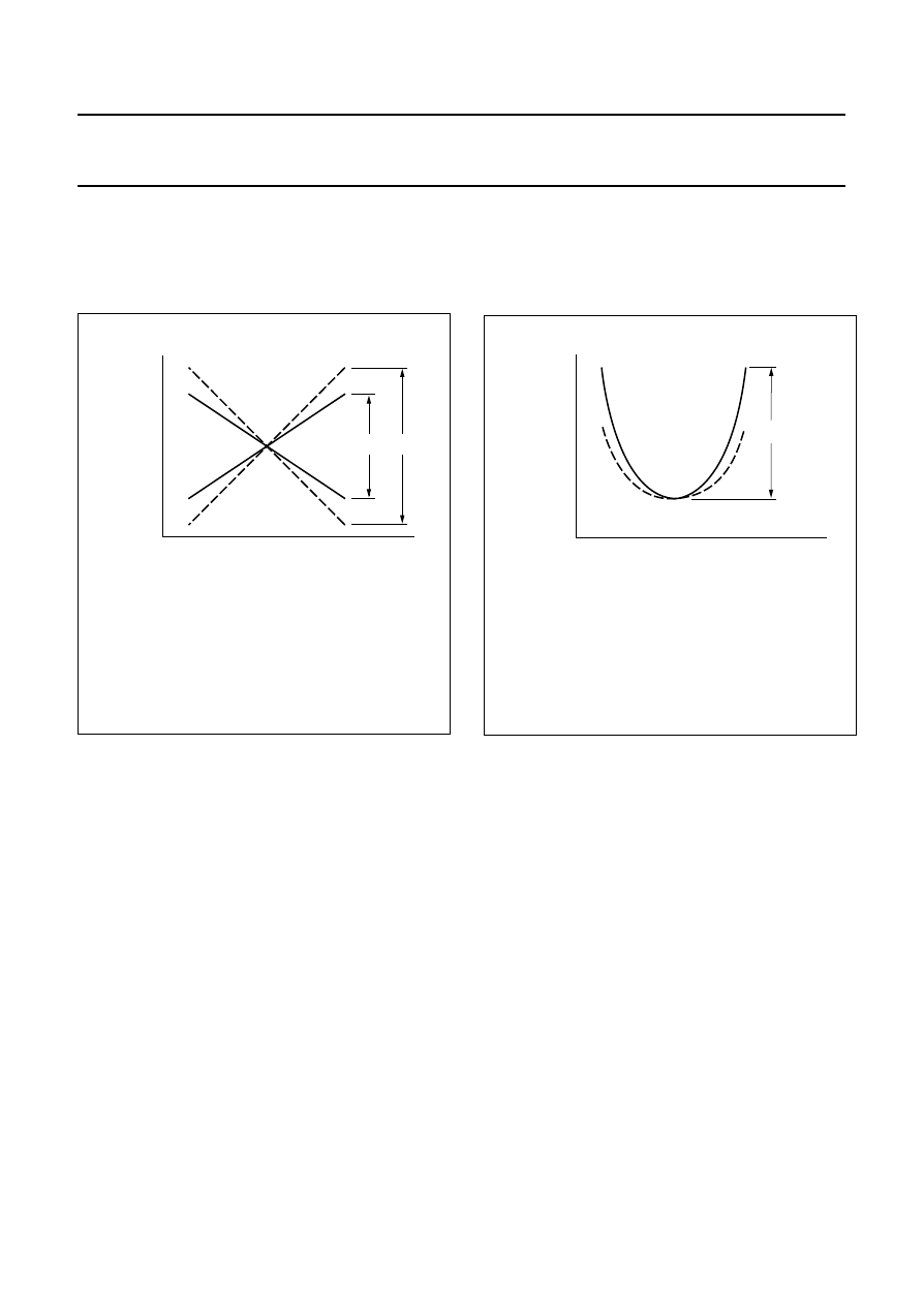
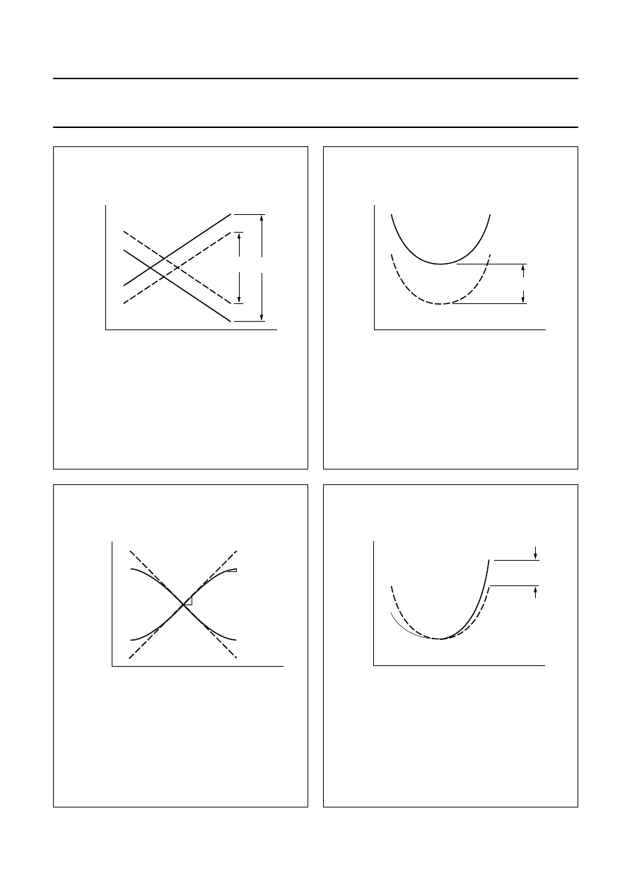
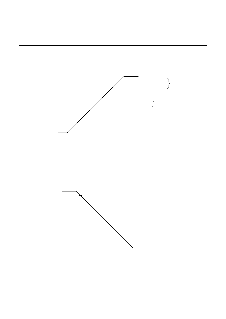
Vertical and EW adjustments
Fig.3 I
VOUT1
and I
VOUT2
as functions of time.
(1)
∆
I
1
is the maximum amplitude setting at VAMP (pin 18); VPOS
centred and VSCOR = 0%.
VAMP
∆
I
∆
2
I
∆
1
--------
100%
×
=
handbook, halfpage
t
IVOUT1
IVOUT2
∆
l2
∆
l1
(1)
MBG590
Fig.4 V
EWDRV
as a function of time.
∆
EWPAR = 0 to V
PAR(EWDRV)
.
handbook, halfpage
t
VEWDRV
VPAR(EWDRV)
MBG591
1996 Jul 18
23
Philips Semiconductors
Preliminary specification
Economy Autosync Deflection Controller
(EASDC)
TDA4858
Fig.5 I
VOUT1
and I
VOUT2
as functions of time.
(1)
∆
I
1
is VPOS adjustment centred; maximum amplitude setting at
VAMP (pin 18).
VPOS
∆
I
2
∆
I
1
∆
–
2
I
1
∆
×
----------------------
100%
×
=
handbook, halfpage
t
IVOUT1
IVOUT2
∆
l2
∆
l1
(1)
MBG592
Fig.6 V
EWDRV
as a function of time.
∆
EWWID = 0 to V
DC(EWDRV)
.
handbook, halfpage
t
VEWDRV
VDC(EWDRV)
MBG593
Fig.7 I
VOUT1
and I
VOUT2
as functions of time.
(1)
∆
I
1
is VSCOR = 0%; maximum amplitude setting at VAMP
(pin 18).
VSCOR
∆
I
∆
1
I
∆
2
–
I
1
∆
----------------------
100%
×
=
handbook, halfpage
t
IVOUT1
IVOUT2
∆
l2
/∆
t
∆
l1
(1)
/∆
t
MBG594
Fig.8 V
EWDRV
as a function of time.
∆
EWTRP =
±
V
TRP(EWDRV)
.
handbook, halfpage
t
VEWDRV
VTRP(EWDRV)
MBG595
1996 Jul 18
24
Philips Semiconductors
Preliminary specification
Economy Autosync Deflection Controller
(EASDC)
TDA4858
Pulse diagrams
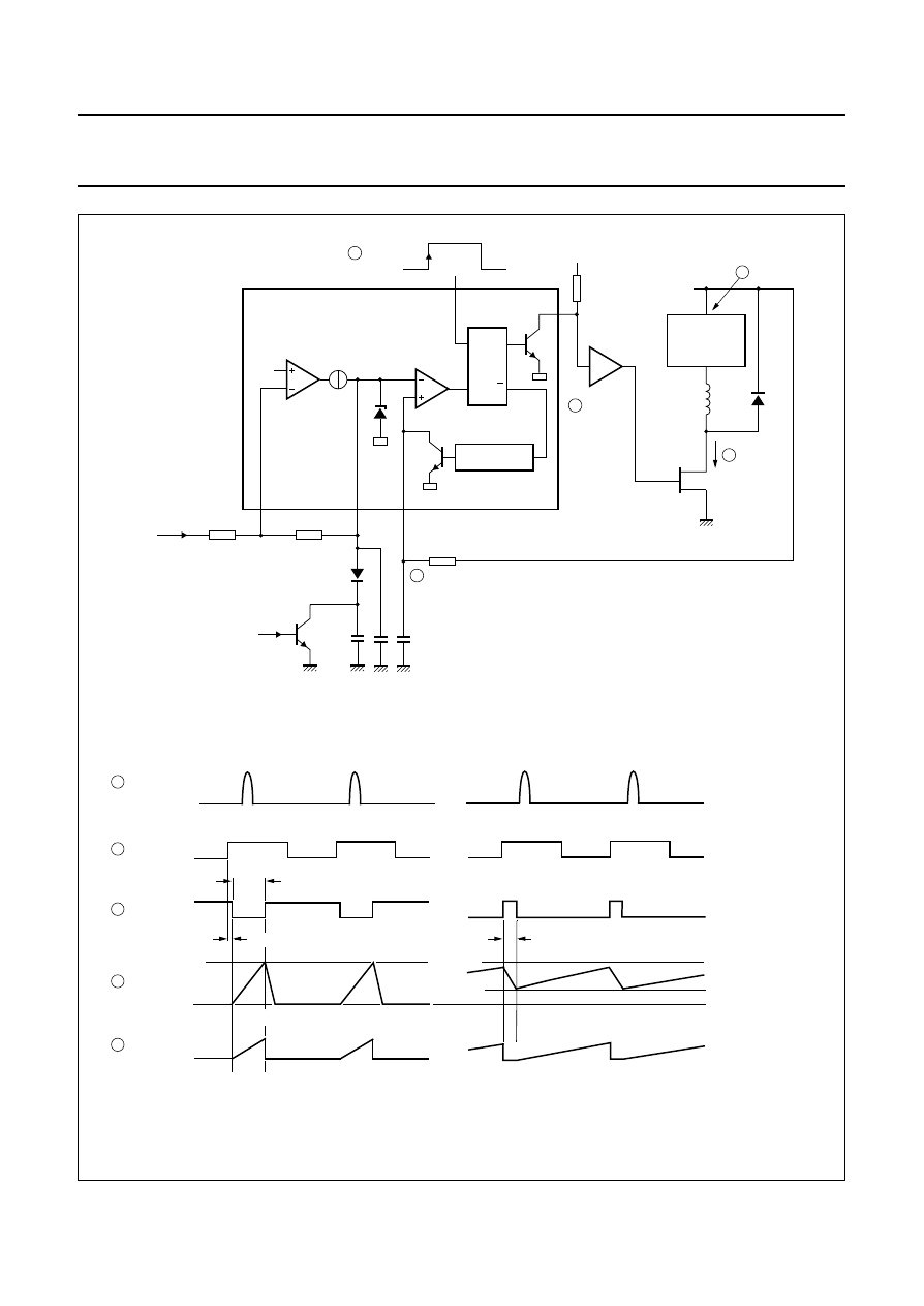
Fig.9 Pulse diagram for horizontal part.
handbook, full pagewidth
+
-
+
–
horizontal sync pulse
PLL2 control current
at HPLL2 (pin 31)
PLL1 control current
at HPLL (pin 26)
line flyback pulse
at HFLB (pin 1)
horizontal oscillator sawtooth
at HCAP (pin 29)
line drive pulse
at HDRV (pin 7)
triggered on
trailing edge of horizontal sync
video clamping pulse
at CLBL (pin 16)
vertical blanking level
triggered on
leading edge of horizontal sync
video clamping pulse
at CLBL (pin 16)
vertical blanking level
PLL2
control range
45 to 48% of line period
MGD096
1996 Jul 18
25
Philips Semiconductors
Preliminary specification
Economy Autosync Deflection Controller
(EASDC)
TDA4858
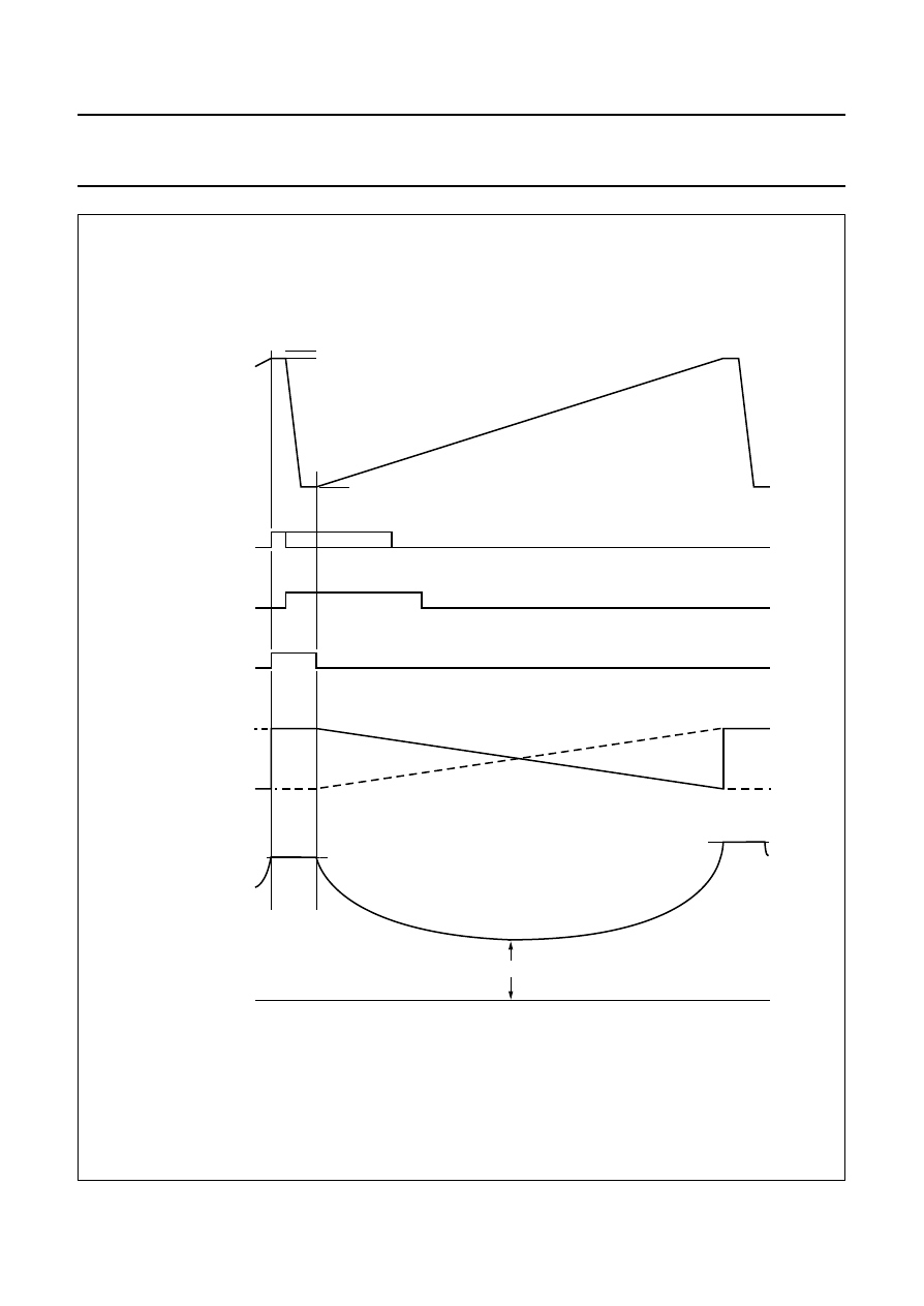
Fig.10 Pulse diagram for vertical part.
handbook, full pagewidth
internal trigger
inhibit window
(typical 6.7 ms)
1.4 V
3.8 V
automatic trigger level
vertical sync pulse
4.0 V
differential output currents
VOUT1 (pin 13) and
VOUT2 (pin 12)
inhibited
vertical oscillator sawtooth
at VCAP (pin 24)
vertical blanking pulse
at CLBL (pin 16)
synchronized trigger level
EW drive waveform
at EWDRV (pin 11)
EW parabola 3 V (p-p) maximum
DC shift 4 V maximum
7.0 V maximum
LOW level 1.2 V fixed
IVOUT1
IVOUT2
MGD097
1996 Jul 18
26
Philips Semiconductors
Preliminary specification
Economy Autosync Deflection Controller
(EASDC)
TDA4858
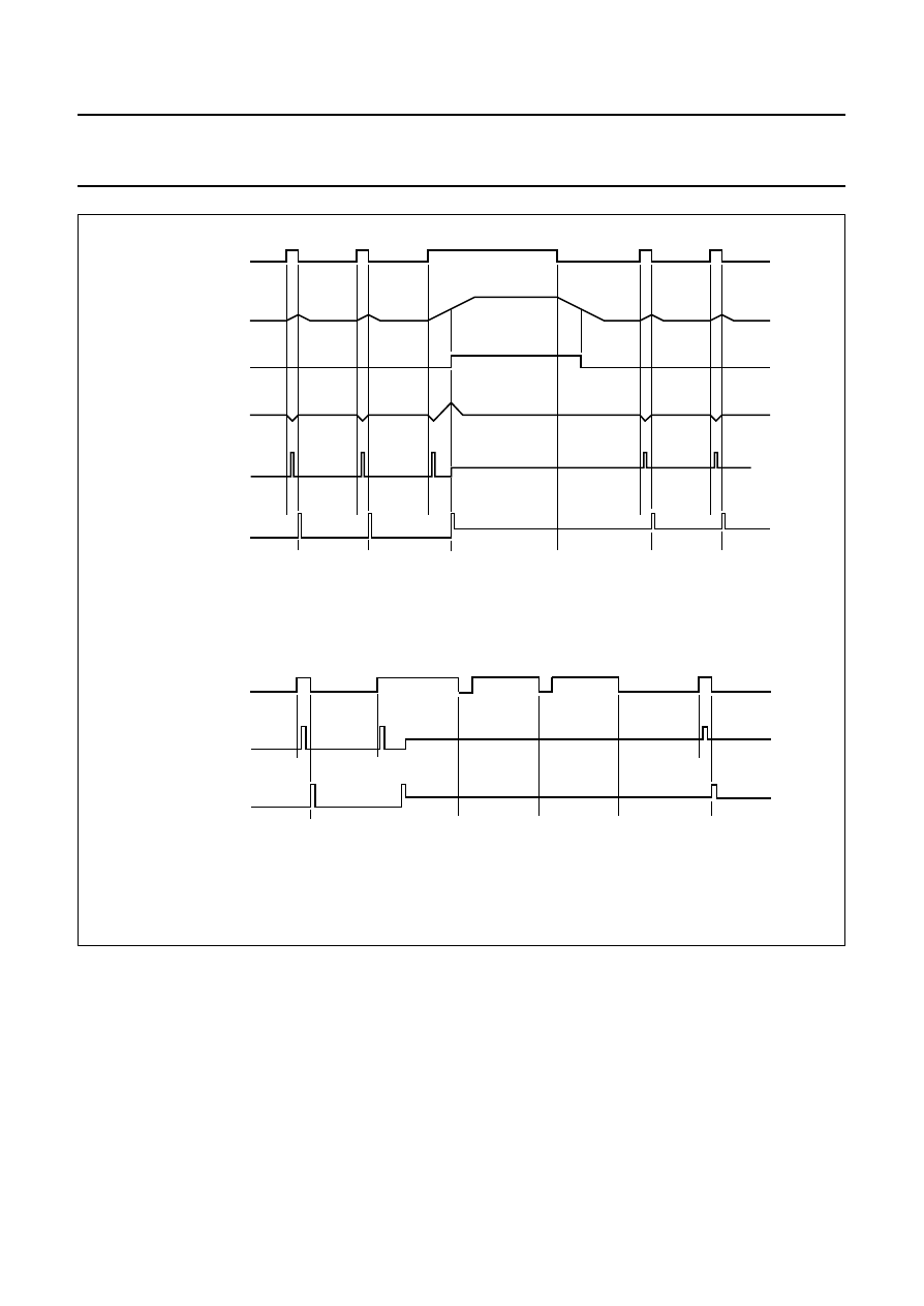
Fig.11 Pulse diagrams for composite sync applications.
a. Reduced influence of vertical sync on horizontal phase.
b. Generation of video clamping pulses during vertical sync with serration pulses.
handbook, full pagewidth
composite sync (TTL)
internal integration of
composite sync
internal vertical
trigger pulse
PLL1 control voltage
at HPLL1 (pin 26)
at HSYNC (pin 15)
pulses at CLBL (pin 16)
(triggered on trailing edge)
clamping and blanking
pulses at CLBL (pin 16)
(triggered on leading edge)
clamping and blanking
MGD098
handbook, full pagewidth
composite sync (TTL)
at HSYNC (pin 15)
clamping and blanking
pulses at CLBL (pin 16)
(triggered on trailing edge)
clamping and blanking
pulses at CLBL (pin 16)
(triggered on leading edge)
MGD099
1996 Jul 18
27
Philips Semiconductors
Preliminary specification
Economy Autosync Deflection Controller
(EASDC)
TDA4858
APPLICATION INFORMATION
Fig.12 Application and timing for feedback mode.
For f < 50 kHz and C2 < 47 nF calculation formulas and behaviour of the OTA are the same as for an OP. An exception is the limited output current at
BOP (pin 3). See Chapter “Characteristics”, Row Head “B+ control section (see Figs 12 and 13)”.
a. Feedback mode application.
b. Waveforms for normal operation.
c. Waveforms for fault condition.
handbook, full pagewidth
DISCHARGE
S
R
Q
Q
HORIZONTAL
OUTPUT
STAGE
VHDRV
VCC
Vi
7
6
D2
TR1
R5
C4
R4
R6
L
OTA
2.5 V
5
VBIN
VBOP
VBSENS
VBDRV
CBOP
D1
R1
R3
EWDRV
C1
R2
C2
3
4
>
4.7 nF
horizontal
flyback pulse
INVERTING
BUFFER
3
2
4
1
MBG599
handbook, full pagewidth
VHDRV
VBSENS
VBSENS = VBOP
VBDRV
toff(min)
ton
horizontal
flyback pulse
VRESTART(BSENS)
VSTOP(BSENS)
2
3
4
1
MBG600
td(BDRV)
1996 Jul 18
28
Philips Semiconductors
Preliminary specification
Economy Autosync Deflection Controller
(EASDC)
TDA4858
Fig.13 Application and timing for feed forward mode.
a. Forward mode application.
b. Waveforms for normal operation.
c. Waveforms for fault condition.
handbook, full pagewidth
DISCHARGE
S
R
Q
Q
HORIZONTAL
OUTPUT
STAGE
VHDRV
VCC
7
6
D2
TR1
R3
R4
OTA
2.5 V
5
VBIN
VBOP
VBSENS
CBSENS
VBDRV
CBOP
R1
R2
C1
D1
TR2
3
4
>
4.7 nF
>
2 nF
horizontal
flyback pulse
INVERTING
BUFFER
3
1
IMOSFET
5
2
4
EHT
transformer
EHT adjustment
power-down
MBG601
handbook, full pagewidth
VBOP
VBOP
VSTOP(BSENS)
toff
VRESTART(BSENS)
VHDRV
VBSENS
VBDRV
horizontal
flyback pulse
2
3
4
IMOSFET
5
1
ton
(discharge time of CBSENS)
MBG602
td(BDRV)
1996 Jul 18
29
Philips Semiconductors
Preliminary specification
Economy Autosync Deflection Controller
(EASDC)
TDA4858
Start-up and shut-down sequence
Fig.14 Start-up sequence and shut-down sequence.
(1) See Fig.15 for PLL2 soft-start.
a. Start-up sequence.
b. Shut-down sequence.
handbook, full pagewidth
VCC
continuous blanking off
PLL2 enabled
frequency detector enabled
8.5 V
5.8 V
PLL2 soft start sequence begins
(1)
4.0 V
continuous blanking CLBL (pin 16) activated
time
8.2 V
video clamping pulse enabled
BDRV enabled
VOUT1 and VOUT2 enabled
VCC
>
8.5 V
and
VHPLL2
>
4.4 V
VCC
>
8.2 V
and
VHPLL2
>
3.7 V
MBG555
handbook, full pagewidth
VCC
continuous blanking CLBL (pin 16) activated
PLL2 disabled
frequency detector disabled
8.5 V
8.0 V
5.6 V
4.0 V
continuous blanking disappears
HDRV floating
time
video clamping pulse disabled
BDRV floating
VOUT1 and VOUT2 floating
MBG554
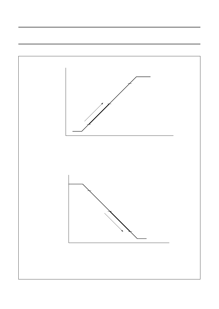
1996 Jul 18
30
Philips Semiconductors
Preliminary specification
Economy Autosync Deflection Controller
(EASDC)
TDA4858
PLL2 soft start sequence
Fig.15 PLL2 soft start sequence.
a. PLL2 start-up sequence.
b. PLL2 shut-down sequence.
handbook, full pagewidth
VHPLL2
continuous blanking off
PLL2 enabled
frequency detector enabled
4.4 V
3.7 V
0.5 V
time
HDRV duty factor begins to increase
HDRV duty factor has reached nominal value
BDRV enabled
VOUT1 and VOUT2 enabled
duty factor increases
MBG553
handbook, full pagewidth
VHPLL2
continuous blanking CLBL (pin 16) activated
PLL2 disabled
frequency detector disabled
4.4 V
3.7 V
0.5 V
time
HDRV floating
HDRV duty factor begins to decrease
BDRV floating
VOUT1 and VOUT2 floating
duty factor decreases
MBG552

1996 Jul 18
31
Philips Semiconductors
Preliminary specification
Economy Autosync Deflection Controller
(EASDC)
TDA4858
Vertical linearity error
Fig.16 Definition of vertical linearity error.
(1) I
VOUT
= I
VOUT1
−
I
VOUT2
.
(2) I
1
= I
VOUT
at V
VCAP
= 1.9 V.
(3) I
2
= I
VOUT
at V
VCAP
= 2.6 V.
(4) I
3
= I
VOUT
at V
VCAP
= 3.3 V.
Which means:
Vertical linearity error =
I
0
I
1
I
3
–
2
--------------
=
1
max
I
1
I
2
–
I
0
-------------- or
I
2
I
3
–
I
0
--------------
–
handbook, halfpage
I1
(2)
I2
(3)
I3
(4)
IVOUT
(1)
(
µ
A)
+
415
−
415
0
VVCAP
MBG551
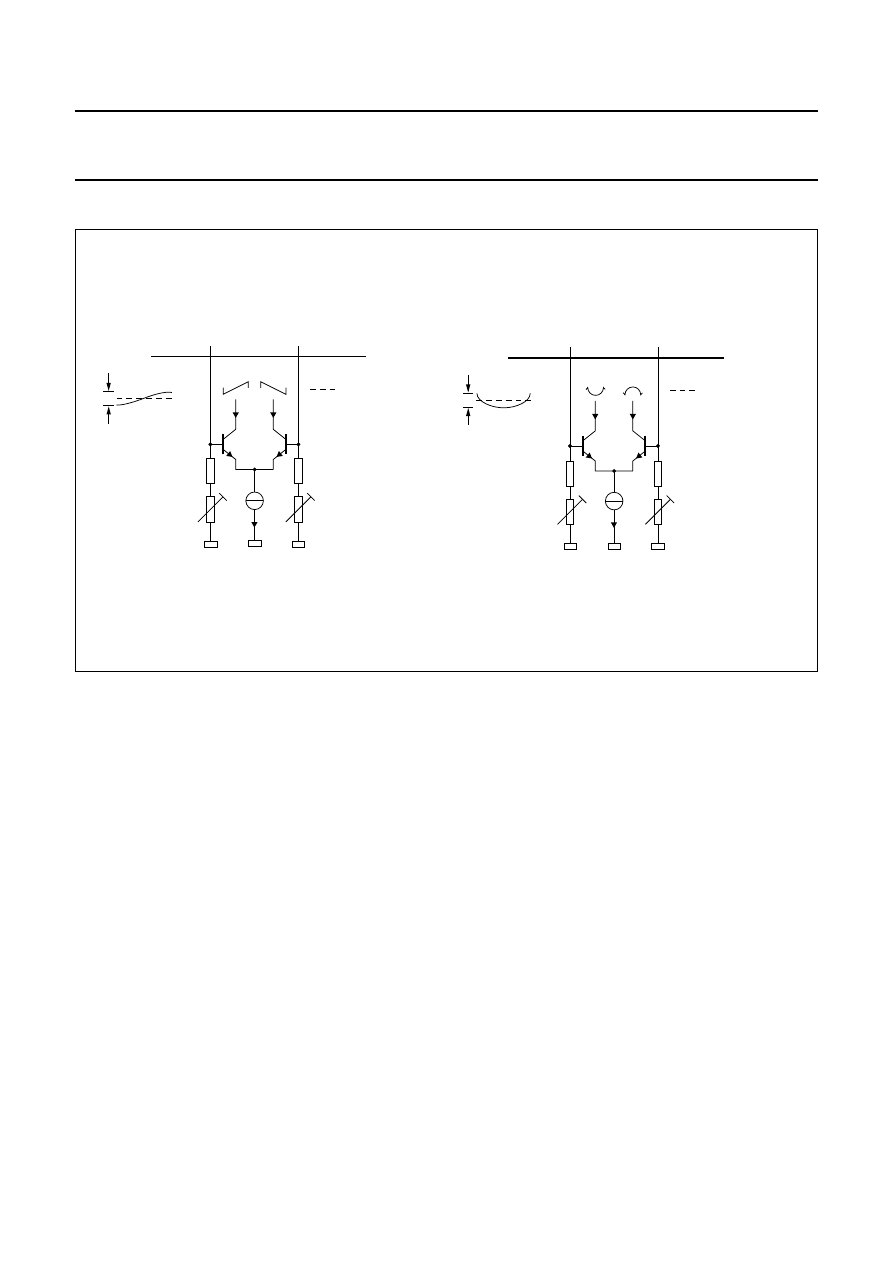
1996 Jul 18
32
Philips Semiconductors
Preliminary specification
Economy Autosync Deflection Controller
(EASDC)
TDA4858
Usage of superimposed waveforms
Fig.17 Superimposed waveforms at pins 19 and 20 with pins 17, 18, 21 or 32.
a. VSCOR (pin 19).
b. EWTRP (pin 20).
handbook, halfpage
VSCOR
VPOS
VAMP
EWPAR
EWWID
17, 18, 21, 32
19
5 V DC
120 mV (p-p)
5 V
MBG556
handbook, halfpage
EWTRP
VPOS
VAMP
EWPAR
EWWID
17, 18, 21, 32
20
5 V DC
5 V
120 mV (p-p)
MBG557
1996 Jul 18
33
Philips Semiconductors
Preliminary specification
Economy Autosync Deflection Controller
(EASDC)
TDA4858
Printed printed-circuit board layout
Fig.18 Hints for printed-circuit board (PCB) layout.
For optimum performance of the TDA4858 the ground paths must be routed as shown. Only one connection to other grounds on the PCB is allowed.
handbook, full pagewidth
TDA4858
1
2
3
4
5
6
7
8
9
10
11
12
13
14
15
16
32
31
30
29
28
27
26
25
24
23
22
21
20
19
18
17
external components of
horizontal section
external components of
driver stages
external components of
vertical section
further connections to other components
or ground paths are not allowed
only this path may be connected
to ground on PCB
MGD100
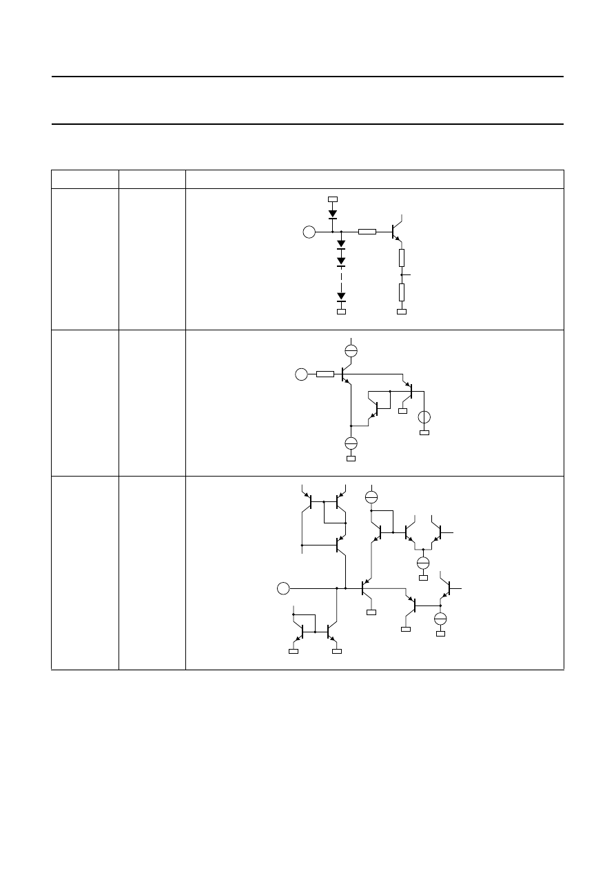
1996 Jul 18
34
Philips Semiconductors
Preliminary specification
Economy Autosync Deflection Controller
(EASDC)
TDA4858
INTERNAL CIRCUITRY
Table 4
Internal circuitry of Fig.1
PIN
SYMBOL
INTERNAL CIRCUIT
1
HFLB
2
XRAY
3
BOP
1.5 k
Ω
7 x
1
MBG561
5 k
Ω
6.25 V
2
MBG562
5.3 V
3
MBG563
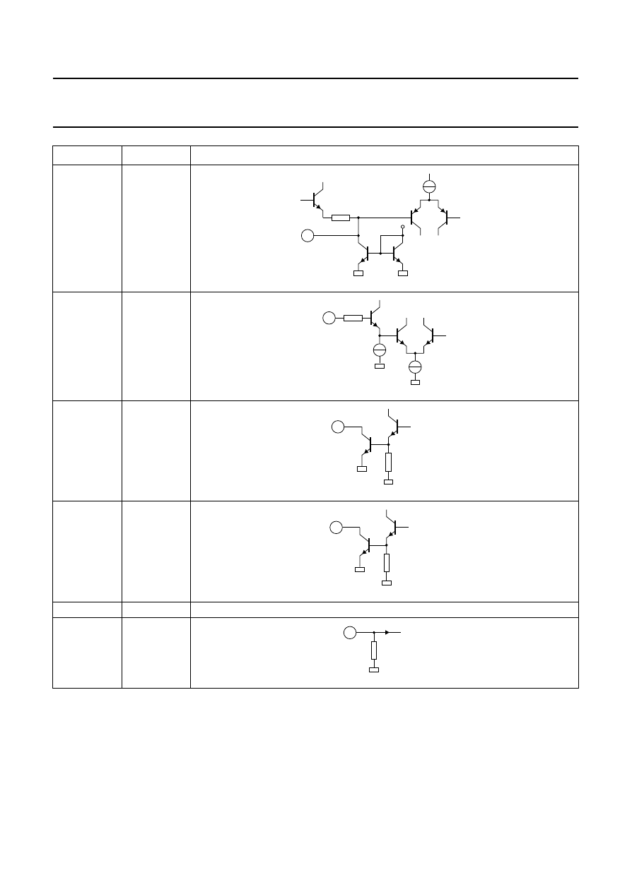
1996 Jul 18
35
Philips Semiconductors
Preliminary specification
Economy Autosync Deflection Controller
(EASDC)
TDA4858
4
BSENS
5
BIN
6
BDRV
7
HDRV
8
PGND
power ground, connected to substrate
9
V
CC
PIN
SYMBOL
INTERNAL CIRCUIT
4
MBG564
5
MBG565
6
MBG566
7
MBG567
9
MBG568
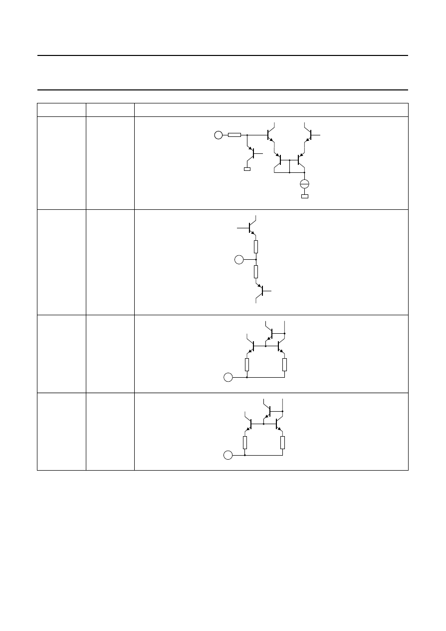
1996 Jul 18
36
Philips Semiconductors
Preliminary specification
Economy Autosync Deflection Controller
(EASDC)
TDA4858
10
CLSEL
11
EWDRV
12
VOUT2
13
VOUT1
PIN
SYMBOL
INTERNAL CIRCUIT
10
6.25 V
80 k
Ω
MGD129
6.25 V
108
Ω
108
Ω
11
MBG570
12
MBG571
13
MBG572
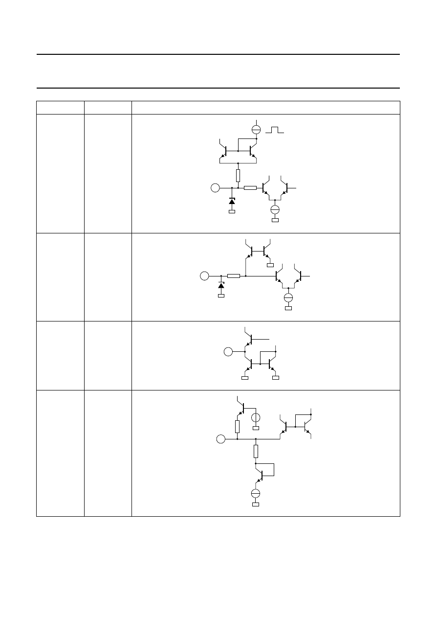
1996 Jul 18
37
Philips Semiconductors
Preliminary specification
Economy Autosync Deflection Controller
(EASDC)
TDA4858
14
VSYNC
15
HSYNC
16
CLBL
17
VPOS
PIN
SYMBOL
INTERNAL CIRCUIT
100
Ω
2 k
Ω
14
7.3 V
1.4 V
MBG573
85
Ω
15
1.4 V
1.28 V
MBG574
16
MBG575
7.2 k
Ω
1 k
Ω
17
5 V
2 VBE
MBG576
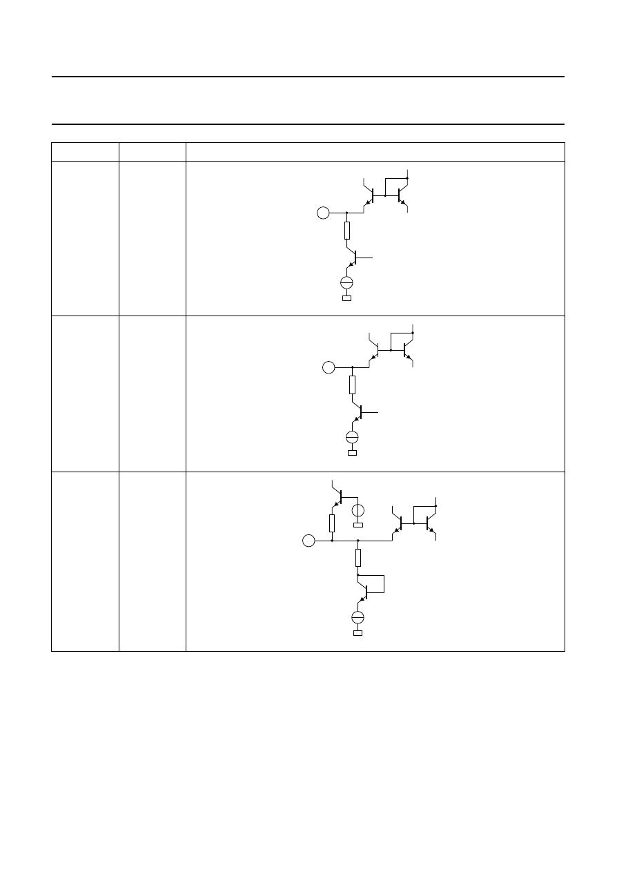
1996 Jul 18
38
Philips Semiconductors
Preliminary specification
Economy Autosync Deflection Controller
(EASDC)
TDA4858
18
VAMP
19
VSCOR
20
EWTRP
PIN
SYMBOL
INTERNAL CIRCUIT
18
5 V
MBG577
19
5 V
MBG578
20
5 V
2 VBE
MBG579
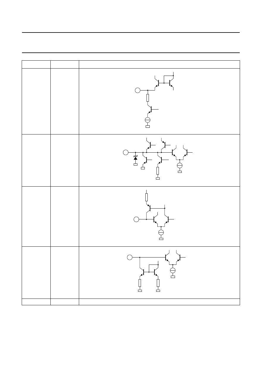
1996 Jul 18
39
Philips Semiconductors
Preliminary specification
Economy Autosync Deflection Controller
(EASDC)
TDA4858
21
EWPAR
22
VAGC
23
VREF
24
VCAP
25
SGND
signal ground
PIN
SYMBOL
INTERNAL CIRCUIT
1 k
Ω
21
5 V
MBG580
22
MBG581
23
3 V
MBG582
24
MBG583
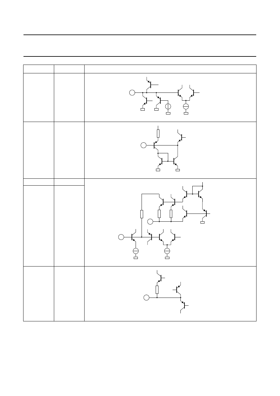
1996 Jul 18
40
Philips Semiconductors
Preliminary specification
Economy Autosync Deflection Controller
(EASDC)
TDA4858
26
HPLL1
27
HBUF
28
HREF
29
HCAP
30
HPOS
PIN
SYMBOL
INTERNAL CIRCUIT
26
5.5 V
MBG589
27
MBG584
76
Ω
28
2.525 V
29
7.7 V
MBG585
1 k
Ω
30
1.7 V
7.7 V
4.3 V
MBG586
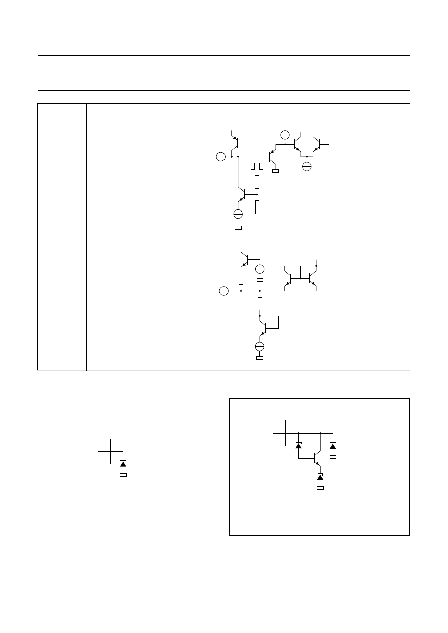
1996 Jul 18
41
Philips Semiconductors
Preliminary specification
Economy Autosync Deflection Controller
(EASDC)
TDA4858
31
HPLL2
32
EWWID
PIN
SYMBOL
INTERNAL CIRCUIT
31
7.7 V
HFLB
MBG587
7.2 k
Ω
1 k
Ω
32
5 V
2 VBE
MBG588
Electrostatic discharge (ESD) protection
Fig.19 ESD protection for pins 4, 10 to 13 and 16.
pin
MBG559
Fig.20 ESD protection for pins 2 to 4, 17 to 24 and
26 to 32.
pin
7.3 V
7.3 V
MBG560
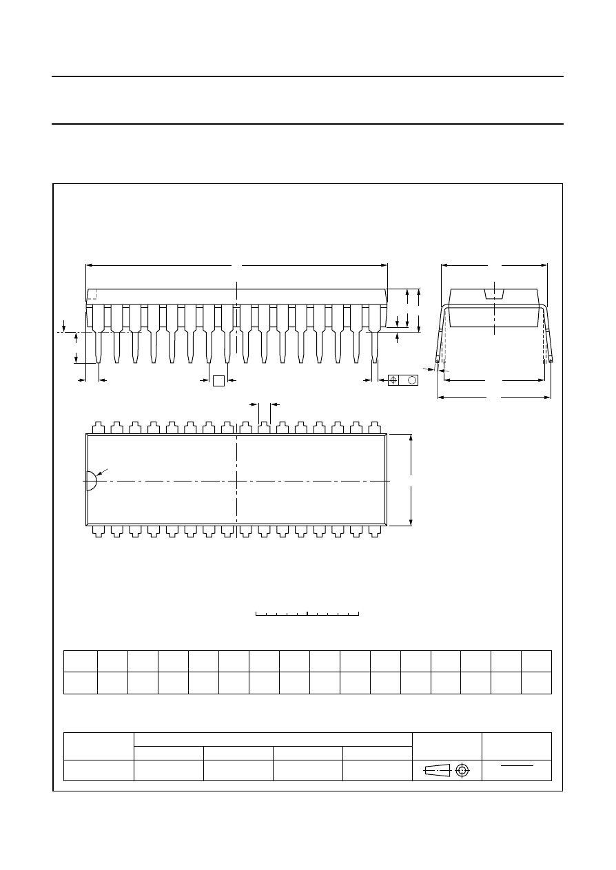
1996 Jul 18
42
Philips Semiconductors
Preliminary specification
Economy Autosync Deflection Controller
(EASDC)
TDA4858
PACKAGE OUTLINE
UNIT
b
1
c
E
e
M
H
L
REFERENCES
OUTLINE
VERSION
EUROPEAN
PROJECTION
ISSUE DATE
IEC
JEDEC
EIAJ
mm
DIMENSIONS (mm are the original dimensions)
SOT232-1
92-11-17
95-02-04
b
max.
w
M
E
e
1
1.3
0.8
0.53
0.40
0.32
0.23
29.4
28.5
9.1
8.7
3.2
2.8
0.18
1.778
10.16
10.7
10.2
12.2
10.5
1.6
4.7
0.51
3.8
M
H
c
(e )
1
M
E
A
L
seating plane
A
1
w
M
b
1
e
D
A
2
Z
32
1
17
16
b
E
pin 1 index
0
5
10 mm
scale
Note
1. Plastic or metal protrusions of 0.25 mm maximum per side are not included.
(1)
(1)
D
(1)
Z
A
max.
1
2
A
min.
A
max.
SDIP32: plastic shrink dual in-line package; 32 leads (400 mil)
SOT232-1

1996 Jul 18
43
Philips Semiconductors
Preliminary specification
Economy Autosync Deflection Controller
(EASDC)
TDA4858
SOLDERING
Introduction
There is no soldering method that is ideal for all IC
packages. Wave soldering is often preferred when
through-hole and surface mounted components are mixed
on one printed-circuit board. However, wave soldering is
not always suitable for surface mounted ICs, or for
printed-circuits with high population densities. In these
situations reflow soldering is often used.
This text gives a very brief insight to a complex technology.
A more in-depth account of soldering ICs can be found in
our
“IC Package Databook” (order code 9398 652 90011).
Soldering by dipping or by wave
The maximum permissible temperature of the solder is
260
°
C; solder at this temperature must not be in contact
with the joint for more than 5 seconds. The total contact
time of successive solder waves must not exceed
5 seconds.
The device may be mounted up to the seating plane, but
the temperature of the plastic body must not exceed the
specified maximum storage temperature (T
stg max
). If the
printed-circuit board has been pre-heated, forced cooling
may be necessary immediately after soldering to keep the
temperature within the permissible limit.
Repairing soldered joints
Apply a low voltage soldering iron (less than 24 V) to the
lead(s) of the package, below the seating plane or not
more than 2 mm above it. If the temperature of the
soldering iron bit is less than 300
°
C it may remain in
contact for up to 10 seconds. If the bit temperature is
between 300 and 400
°
C, contact may be up to 5 seconds.
DEFINITIONS
LIFE SUPPORT APPLICATIONS
These products are not designed for use in life support appliances, devices, or systems where malfunction of these
products can reasonably be expected to result in personal injury. Philips customers using or selling these products for
use in such applications do so at their own risk and agree to fully indemnify Philips for any damages resulting from such
improper use or sale.
Data sheet status
Objective specification
This data sheet contains target or goal specifications for product development.
Preliminary specification
This data sheet contains preliminary data; supplementary data may be published later.
Product specification
This data sheet contains final product specifications.
Limiting values
Limiting values given are in accordance with the Absolute Maximum Rating System (IEC 134). Stress above one or
more of the limiting values may cause permanent damage to the device. These are stress ratings only and operation
of the device at these or at any other conditions above those given in the Characteristics sections of the specification
is not implied. Exposure to limiting values for extended periods may affect device reliability.
Application information
Where application information is given, it is advisory and does not form part of the specification.
Wyszukiwarka
Podobne podstrony:
TDA4851(1)
TDA4850(1)
TDA4850
TDA4855(1)
TDA4857PS
TDA4853 4854(1)
TDA4853 TDA4854(1)
TDA4858
TDA4852
TDA4856 2(1)
więcej podobnych podstron