114
PRZEGLĄD ELEKTROTECHNICZNY, ISSN 0033-2097, R. 84 NR 8/2008
Krzysztof WANDACHOWICZ, Konrad DOMKE
Poznan University of Technology
Measurements of the temperature-dependent changes of the
photometrical and electrical parameters of LEDs
Abstract. In addition to emitting light, high power light emitting diodes also generate a significant quantity of heat. Heat released in the p-n junction
of the semiconductor material markedly increases its temperature and thus indirectly affects the photometric and electric characteristics of LEDs.
This paper presents a test stand designed for measuring such characteristics for a wide range of changes of junction temperatures. Junction
temperature adjustment can proceed independently of the thermal power released in the LED.
Streszczenie.
Wytwarzaniu światła w diodach towarzyszy wydzielanie dużej ilości ciepła. Wydzielające się w złączu p-n materiału
półprzewodnikowego ciepło zwiększa znacząco jego temperaturę i wpływa pośrednio na zmianę charakterystyk fotometrycznych i elektrycznych
diody. W pracy przedstawiono stanowisko badawcz
e pozwalające mierzyć te charakterystyki dla szerokiego zakresu zmian temperatury złącza.
Regulacja temperatury złącza może przy tym przebiegać niezależnie od wydzielanej w diodzie mocy cieplnej. (Pomiar wpływu temperatury złącza
p-n na parametry fotometryczne i elektryczne diod elektroluminescencyjnych).
Keywords: light emitting diode, junction temperature, photometric measurements.
Słowa kluczowe: dioda elektroluminescencyjna, temperatura złącza p-n, pomiary fotometryczne.
Introduction
In addition to emitting light, LEDs also generate a
significant quantity of heat. The assumption is that ca. 75%
of total power is released in the form of heat which must be
carried into the environment. Heat released in the p-n
junction of the semiconductor material markedly increases
its temperature and thus indirectly affects the photometric
and electric characteristics of LEDs.
A thorough examination of LED properties is required to
construct a luminaire system or vehicle lights with preset
input parameters. A factor of basic significance is the
relationship between electric/photometric parameters and
the working temperature T
j
of the p-n junction. Specification
sheets for light emitting diodes provide electric parameters
(forward voltage U
F
) and photometric parameters (luminous
flux
, colour temperature T
C
, chromaticity coordinates xy)
for a set value of the forward current I
F
in the p-n junction
working temperature T
j
of 25
0
C, whereas typical operating
temperature T
j
of the p-n junction in HP LEDs (with the
power value of several watts) exceeds 100
0
C. As the
temperature of the p-n junction rises, luminous flux
and
forward voltage U
F
values drop, accompanied by a shift of
the wavelength
m
representing maximum spectral
distribution
to
a
higher
wavelength.
Luminaire
manufacturers use a variety of means to reduce the
temperature T
j
of the p-n junction. LEDs are typically
installed on heatsinks which, by substantially improving the
process of transferring heat generated in the p-n junction
into the environment, reduce the temperature T
j
of the
junction.
LED structure
Semiconductor LEDs made in the solid state lighting
(SSL) technology can be divided into low power (LEDs) and
high power (HP LEDs). LEDs are p-n junction devices
constructed of different materials (GaAs, GaAsP, GaP,
AlInGaP, InGaN). The junction in a LED is forward biased
and when electrons cross the junction from the n- to the p-
type material, the electron-hole recombination process
produces some photons in the UV, IR or VIS in a process of
electroluminescence (radiative recombination). In non-
radiative recombination events, the energy released during
the electron-hole recombination is converted to phonons.
Phonon is a quantised mode of vibration occurring in a rigid
crystal lattice that increase temperature and produce heat.
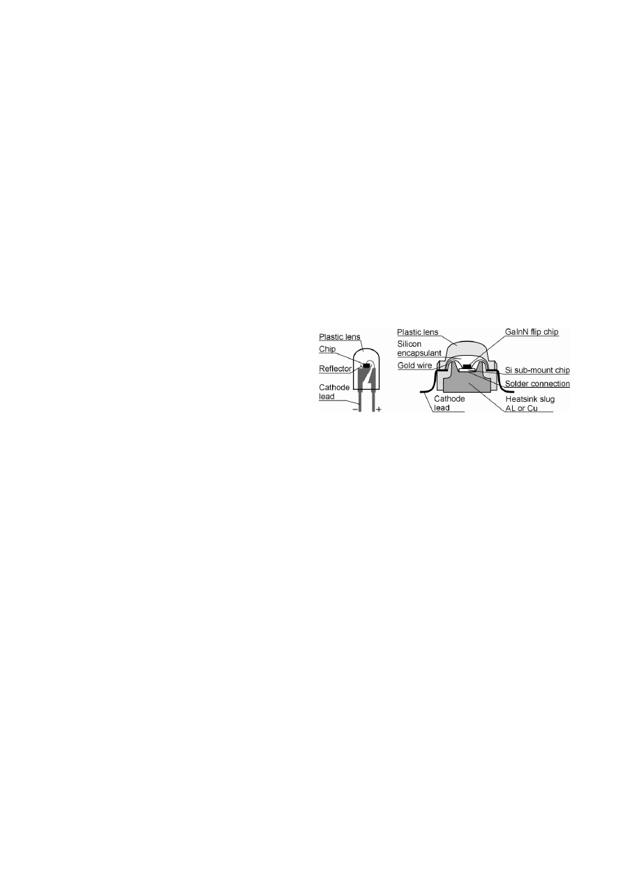
A typical design of low and high power light emitting diodes
is shown in figure 1.
a) b)
Fig. 1. Structure of LED: a) low power, b) high power.
Low power diodes are usually made in the through-hole
technology and operate without additional heatsink slugs.
High power light emitting diodes (HP LEDs) made in the
surface mount technology (SMT) have a different design.
LEDs of this type, are designed in such a way as to allow
easy take away heat from the p-n junction to the metal
diode base, as illustrated in Fig. 1b. HP LEDs are usually
placed on a metal core printed circuit board (MCPCB), often
with an additional heatsink slug. Currently manufactured
LEDs are generally installed on MCPCB sections and they
are assembled in the finished product (e.g. in a luminaire)
by mechanical fastening to the heatsink surface.
Heat flow in LEDs
Processes taking place in HP LEDs generate a
considerable amount of heat. Most of the heat is released in
the p-n junction during the flow of the forward current I
F
.
Joule heat generated in voltage conductors supplying
voltage to the p-n structure is practically negligible. A
characteristic feature to note is the small area S (volume of
the p-n structure) which produces heat. This results in very
high heat power densities q and consequent difficulties with
dissipating such large amounts of heat. Table 1 is illustrated
lists of data for standard currently manufactured LEDs.
Heat generated in the junction must be carried into the
environment. Initially, some heat is dissipated as a result of
thermal conduction via internal LED components from the
p-n structure area to the external LED components (e.g. to
the MCPCB base). A description of the phenomenon is
based on the notion of the so-called thermal resistance R
th
.
Thermal resistance Hewitt and Wong [5, 6] define as:
PRZEGLĄD ELEKTROTECHNICZNY, ISSN 0033-2097, R. 84 NR 8/2008 115
(1)
th
y
x
y
x
,
th
P
T
T
R
where: T
x
, T
y
– temperatures of x or y surfaces, P
th
- thermal
power flowing between those surfaces.
Table 1. Standard HP LED specifications [2, 3, 4].
LED type
P=U
F
I
F
[W]
Efficiency
[%]
Heat power
P
th
=(1-
) P
[W]
T
j
[
o
C]
Heat power
dens q=P
th
/S
[W/m
2
]
C460XB900
-S92xx-A
1.2
14
0.98
125
1.410
6
EZ1000
3.8
28
2.7
145
3.110
6
OSTAR
LEWE3A
27
28
19.4
150
2.910
6
In HP LEDs the direction of the main heat flux is from
the p-n junction to the metal heatsink slug and to metal
anode and cathode leads soldered to the PCB base. The
heat flux through non-metallic elements of the diode to the
external epoxy housing and the lens accounts for no more
than 1% of P
th
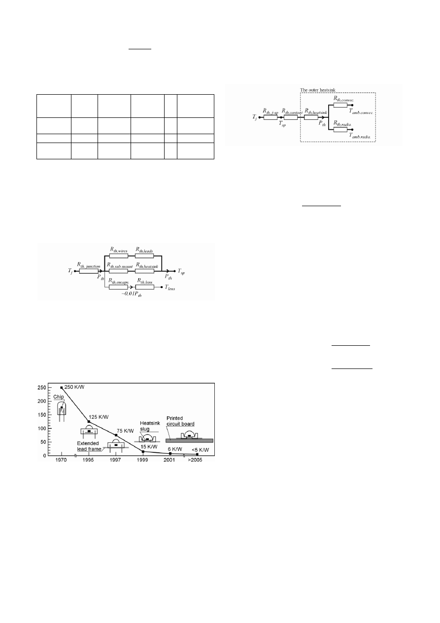
and can be disregarded [1]. Resistances R
th
which occur in the internal heat flow path are referred to as
internal thermal resistances. A connection diagram for
thermal resistances inside a LED is shown in figure 2.
Fig. 2. Diagram for internal thermal resistances of LEDs. Main heat
flow paths are marked with bold lines.
T
sp
– temperature measured
on LED body at the so called solder point.
LED internal thermal resistances are difficult to measure
and are strictly related to the internal design of specific LED
types. Diode manufacturers are striving to work out designs
with reduced thermal resistance levels. Reductions in R
th,j-sp
levels resulting from modifications in LED design are shown
in figure 3.
Fig. 3. Thermal resistance of LED packages
R
th,j-sp
(adopted from
Arik et al., 2002).
Manufacturers generally specify only the total thermal
resistance R
th,j-sp
measured between the semiconductor
junction inside the diode and its metallic core [2, 3, 4]. In
order to ensure adequate cooling of HP LEDs, the base of
the diode is soldered or fastened (e.g. screwed down) to a
suitable outer heatsink with thermal resistance R
th,heatsink
.
Thermal power P
th
is carried from the heatsink surface:
by convection to the gas surrounding the heatsink (with
temperature T
amb.convec.
) and by radiation to other bodies
surrounding the heatsink (with temperature T
amb.radia.
).
Corresponding thermal resistances are marked as R
th,convec.
and R
th,radia.
. In specific cases, temperatures T
amb.convec.
and
T
amb.radia.
can differ. Heatsink manufacturers usually specify
total thermal resistance R
th,heatsink-amb.
and recommend
assuming that T
ambient
= 0.5(T
amb.convec.
+ T
amb.radia.
).
Fig. 4. Diagram for thermal resistances of a LED installed on the
outer heatsink.
The external heatsink is intended to dissipate the
thermal power Pth from the diode into the environment. It
can be calculated using the formula below:
(2)
.
tot
,
th
ambient
j
th
R
T
T
P
)
(
P
1
where: P=U
F
∙I
F
– power of total electric losses on the diode,
- efficiency, R
th,tot.
- total thermal resistance between the p-
n junction and the environment with the temperature T
ambient
.
(3)
.
amb
heatsink
,
th
contact
,
th
sp
j
,
th
.
tot
,
th
R
R
R
R
where: R
th,heatsink-amb.
- total thermal resistance of the heatsink,
R
th,contact
– thermal resistance of the LED-heatsink
connection.
The specifications are provided by manufacturers and
are the basic factors determining heatsink choice. The
formulas given in (2) and (3) show that heatsinks should be
selected in such a way as to make the total thermal
resistance satisfy the relationship (4).
(4)
th
ambient
sp
contact
,
th
.
amb
heatsink
,
th
sp
j
,
th
th
ambient
j
contact
,
th
.
amb
heatsink
,
th
P
T
T
R
R
R
P
T
T
R
R
Test stand
The basic aim of constructing the test stand was to
create appropriate conditions for performing LED tests
focused on electric and photometric characteristics in the
function of the variable temperature T
j
of the p-n junction,
with a constant, freely set value of forward current intensity
I
F
. In order to achieve the objective, it was necessary to
come up with a system which, in addition to standard
measurements of electric and photometric parameters,
would also ensure adjustable inflow or outflow of thermal
power P
th
to the p-n junction. LEDs selected for testing were
mounted on a metallic MCPCB base with high thermal
conductivity
. The base is fastened to the metal core block
(Cu), with a Peltier element placed on the opposite surface
(see figure 5).
When voltage is applied the Peltier element, the current
I
Plt
is generated, producing a temperature difference which
is conducive to the flow of thermal power P
th
from the LED
to the heat exchanger. Therefore, the Peltier element acts
as a pump with adjustable delivery rate, transferring thermal
power from the LED to the heat exchanger. The heat
exchanger is connected with external cooling system, which
is based on liquid cooling radiator placed in a freezer. The
pump forced circulation of cooling liquid with ability of
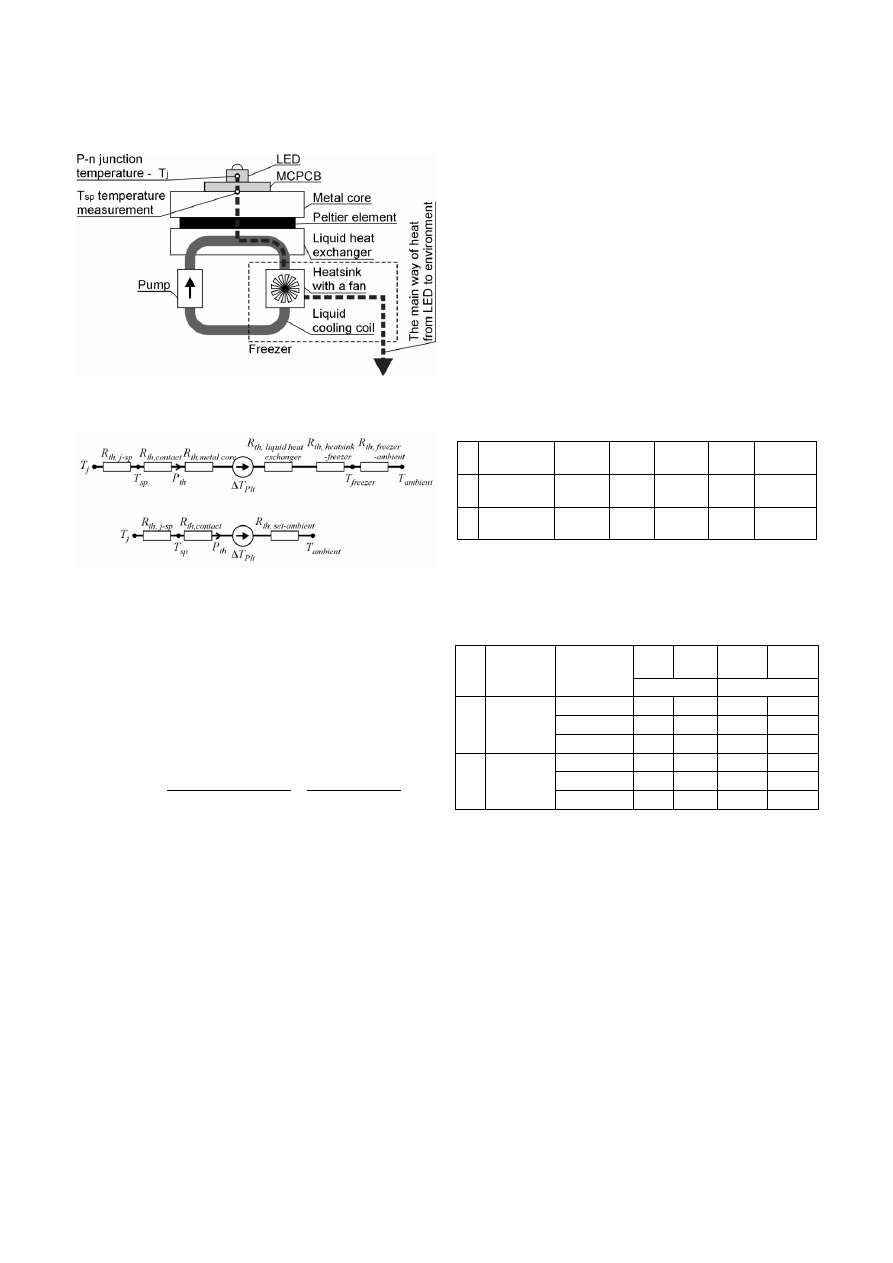
116
PRZEGLĄD ELEKTROTECHNICZNY, ISSN 0033-2097, R. 84 NR 8/2008
changing its velocity. The main way of heat flow from p-n
junction to environment is shown in figure 5. A connection
diagram of thermal resistances of the test stand is
presented below (figure 6).
Fig. 5. Diagram illustrating the test stand designed for performing
tests of thermal characteristics of light emitting diodes.
Fig. 6. Diagram for thermal resistances of the test stand: full and
simplified.
In figure 6, the Peltier element is shown as a source of
temperature difference
T
Plt
(equivalent to the source of
voltage) produced by the flow of current with the current
intensity I
Plt
. The value of
T
Plt
can be adjusted by changes
in the current intensity I
Plt
, while the sign of the temperature
difference
– its direction. Consequently, by changing the
polarity of voltage applied to the Peltier element, you may
obtain an effect of p-n junction cooling or heating. Analysing
the thermal circuit given in figure 6, you derive the following:
(5)
ambient
set
,
th
ambient
Plt
contact
,
th
sp
j
,
th
Plt
j
th
R
T
T
R
R
T
T
P
2
1
(6)
ambient
Plt
ambient
set
,
th
contact
,
th
sp
j
,
th
th
j
T
T
)
R
R
R
(
P
T
where:
T
Plt
=T
Plt1
-T
Plt2
-the temperature difference produced
on the Peltier element.
Analysing the formula in (6), it follows that it is possible
to obtain a preset junction temperature at any power P
th
by
selecting an appropriate value of
T
Plt
=f(I
Plt
). The
temperature is obtained without interfering with the power
P
th
generated in the diode. Given the sufficient efficiency of
the Peltier element, it is possible to achieve junction
temperatures that are lower than the ambient temperature.
The test stand described here thus makes it possible to
obtain preset junction temperatures for a broad range of
changes of thermal power generated in the LED. P
th
and T
j
can be adjusted independently. The temperature of the
junction T
j
was determined indirectly, using the formula:
(7)
sp
F
F
sp
j
,
th
sp
th
sp
j
,
th
j
T
I
U
)
(
R
T
P
R
T
1
where: T
sp
- temperature measured in the central point at
the contact surface of the LED’s MCPCB with the metal
core of the test stand (figure 5).
Temperature measurements were performed using a K
thermocouple (Ø 0.2 mm) in the steady thermal state. The
value of thermal resistance R
th,j-sp
was assumed according to
the manufacturer's specifications. Thermal power was
defined on the basis of measurements of LED electric
parameters. The use of the formula given in (7) to
determine the junction temperature T
j
is recommended,
however manufacturers assumes that thermal resistance
R
th,j-sp
was determined for total power supplied to the diode
P
th
=U
F
∙I
F
.
Measurements
Measurements were carried out for two types of light
emitting diodes [2, 3, 4] (table 2).
Table 2. Catalogue specifications of light emitting diodes: maximum
permitted values are given in brackets.
No
LED type
I
F
[mA]
U
F
[V]
[lm]
T
j
[
0
C]
R
th,j-sp
[K/W]
1
K2 Star
L2K2-MWW4
1000
(1500)
3,72
100
110
(150)
13
2
Ostar
LE W E3A
700
(1000)
20,8
240 ÷
520
150
(180)
3
The test stand made it possible to obtain a wide range
of temperatures to measure temperature characteristics of
the examined diodes (table 3).
Table 3. Minimum and maximum values of temperatures T
j
and T
sp
obtained in test stand.
Lp
LED type
I
F
[mA]
T
j
[C]
T
sp
[C]
T
j
[C]
T
sp
[C]
min
max
1
K2 Star
L2K2-
MWW4
1000
31
-22
166
118
700
18
-17
169
138
350
-12
-28
167
152
2
Ostar
LE W E3A
700
34
-6
173
134
500
19
-10
175
149
350
7
-12
175
157
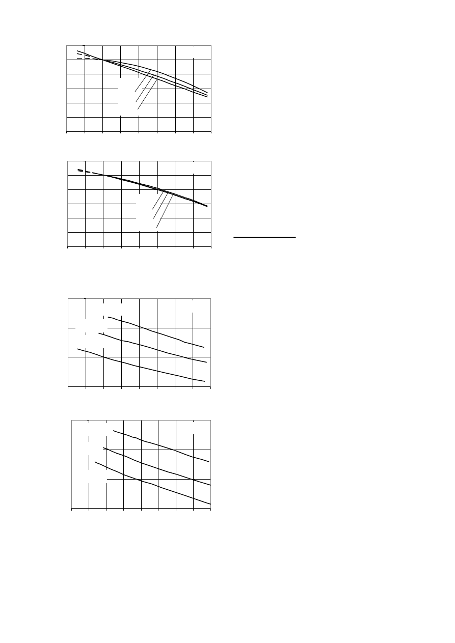
Sample results showing changes of the luminous flux
and the forward voltage U
F
in the function of junction
temperature are given in figure 7 and figure 8. The
characteristics corroborate the relationship between the
luminous flux and the temperature of the junction. For
recommended maximum operating temperatures of the p-n
junction (110
0
C and 150
0
C), flux reduction
– in relation to
catalogue specifications
– is considerable, amounting to
20%÷31% (K2 Star) and 37% (Ostar). The extrapolation of
measurement curves for low temperature (broken lines in
figure 7) resulted from the impossibility to achieve the
assumed temperature of the p-n junction, despite obtaining
negative temperature at the solder point T
sp
. The Peltier
element was not adequately efficient and the value of the
temperature difference
T
Plt
proved insufficient. The defect
will be eliminated in the subsequent version of the test
stand.
PRZEGLĄD ELEKTROTECHNICZNY, ISSN 0033-2097, R. 84 NR 8/2008 117
K2 Star
0
20
40
60
80
100
120
-25
0
25
50
75
100
125
150
175
T
j
[C]
T
/
T=
2
5
C
I
F
1.0A
0.7 A
0.35 A
Ostar
0
20
40
60
80
100
120
-25
0
25
50
75
100
125
150
175
T
j
[C]
T
/
T=
2
5
C
I
F
0.7A
0.5 A
0.35 A
Fig 7. Relative changes of the thermal flux in the function of the
junction temperature T
j
for different values of forward current I
F
.
K2 Star
3,0
3,5
4,0
4,5
-25
0
25
50
75
100
125
150
175
T
j
[C]
U
F
[V
]
I
F
=1.0A
I
F
=0.7A
I
F
=0.35A
Ostar
17,0
18,0
19,0
20,0
-25
0
25
50
75
100
125
150
175
T
j
[C]
U
F
[V
]
I
F
=0.7A
I
F
=0.5A
I
F
=0.35A
Fig 8. Changes of the forward voltage U
F
in the function of the
junction temperature T
j
for different values of forward current I
F
.
Figure 8 presents the temperature characteristics of
changes in the forward voltage U
F
of selected diodes.
Within the range of p-n junction temperature changes
between 50
0
C and 150
0
C, the mean coefficient of forward
voltage change was about 4 mV/
0
C (K2 Star) and 8 mV/
0
C
(Ostar). In view of the typical voltage-current characteristic
of LEDs, where minor changes of the forward voltage U
F
produce major changes of the forward current intensity I
F
,
diode supply should be provided in the form of systems of
stabilised current supplies, not voltage supplies.
REFERENCES
[1] A. A. Efremov, N. I. Bochkareva, R. I. Gorbunov, D. A.
Lavrinovich, Yu. T. Rebane, D. V. Tarkhin, Yu. G. Shreter:
Effect of Joule Heating on the Quantum Efficiency and Choice
of Thermal Conditions for High Power Blue InGaN/GaN LEDs.
Semiconductors. 2006, vol.40, No 5, pp.6005-610.
[2] Cree EZ 000 LEDs.
http://www.cree.com/products/pdf/CPR3CR.pdf
[3] Ostar Lighting: http://www.osram-os.com
[4] Philips Lumileds: http://www.lumileds.com
[5] Hewitt G. F., Shires G. L., Bott T.R.: Process Heat Transfer,
CRC Press, Boca Raton, N. York, 1994.
[6] Wong K-F. V.: Intermediate Heat Transfer. Marcel Dekker Inc.
N. York, 2003.
Authors:
dr inż. Krzysztof Wandachowicz,
E-mail: Krzysztof.Wandachowicz@put.poznan.pl;
dr hab. inż. Konrad Domke, prof. PP,
E-mail: Konrad.Domke@put.poznan.pl;
Poznan University of Technology, Institute of Electrical Engineering
and Electronics, Piotrowo 3a, 60-
965 Poznań, Poland.
Wyszukiwarka
Podobne podstrony:
The Measure of a Marriage
[S] Anne Regentin The Measure of a Man ( c)
[S] Anne Regentin The Measure of a Man
[Friedrich Schneider] Size and Measurement of the Informal Economy in 110 Countries Around the Worl
Guide to the properties and uses of detergents in biology and biochemistry
A Chymicall treatise of the Ancient and highly illuminated Philosopher
Sterne The Life and Opinions of Tristram Shandy, Gentleman
SHSBC418 The Progress and Future of Scientology
Osho (text) Zen, The Mystery and The Poetry of the?yon
Comparison of the Russians and Bosnians
ebook Martial Arts The History and Philosophy of Wing Chun Kung Fu
Herrick The History and Theory of Rhetoric (27)
Becker The quantity and quality of life and the evolution of world inequality
Out of the Armchair and into the Field
The Disproof and proof of Everything
The positive and negative?fects of dna profiling
Cantwell Aids The Mystery And The Solution The New Epidemic Of Acquired Immune Deficiency Syndrom
więcej podobnych podstron