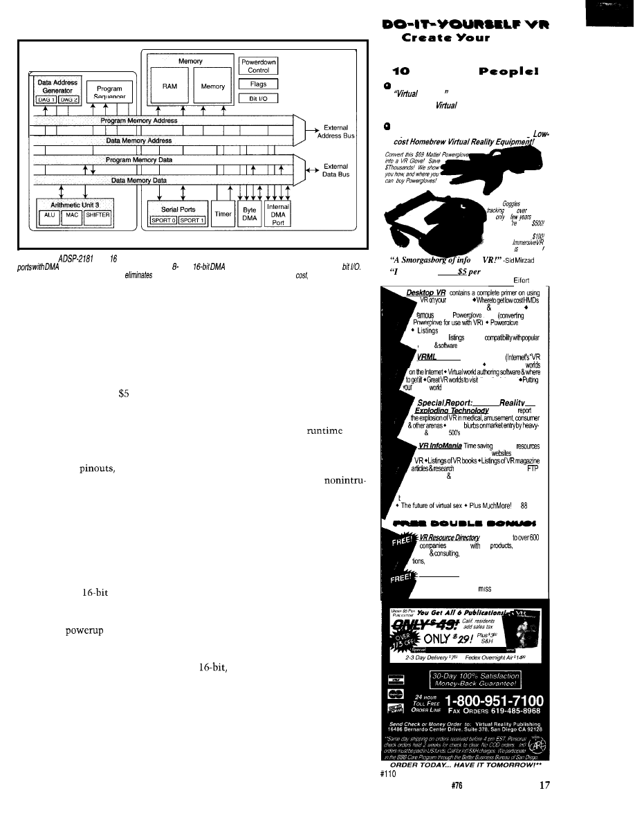
1 4
Building a High-Performance DSP System
by Bob Fine
2 0
Real-Time DSP Modems with a PC and Sound Card
by
Park Brian
3 0
Algorithms and Software for V.34 Modems
by Frank Gao
3 4
Empowered Digital Filtering
by Brian Senese
4 0
Winners of the 8th Annual Circuit Cellar Design Contest
compiled by Elizabeth
4 2
Self-Tuning PD Algorithm for the
68HCll
by Kenneth Baker
4 8
Getting Started with Xilinx
Part
3:
Hands-On Project-Implementation
by David Rector
5 8
The Thrifty Engineer
by Daniel Nygren
6 8
q
From the Bench
Tools
Part 1: Schematic Capture-the Proverbial
Electronic Napkin
Jeff
Bachiochi
7 4
q
Silicon Update
Flash Fight Flares
Tom Can
Task Manager
Ken Davidson
Let Me Ask You
a Dumb Question
R e a d e r
Letters to the Editor
edited by Harv Weiner
Advertiser’s Index
Circuit Cellar INK@
Issue
November 1996
BILL COMES THROUGH
In my article on SDS software (“The Evaluation Board
Saga Continues,”
I mentioned the consequences
of sending SDS a fax asking for help in my microproces-
sor classes. I received some excellent demo software that
I used in my class and in the development of a book.
Since that fax produced so much, I concluded by musing
about what would happen if I sent one to Microsoft.
Bob Davidson at Microsoft read the article and got the
ball rolling. The marvelous result was a generous
donation by Microsoft of NT server and client software,
along with Visual Basic and Visual C++. Also included
were memberships to
and Microsoft Developer
Network and training materials. The total value of these
materials at current
discounts is $34,042
[U.S.).
We are very pleased to receive this donation. Many
thanks to Microsoft and to Todd
Manager of
University Research Programs at Microsoft, for his help
in providing this donation to the University of Calgary.
Mike Smith
Contacting Circuit Cellar
We at Circuit Cellar Mencourage communication between
our readers and our staff, so we have made every effort to make
contacting us easy. We prefer electronic communications, but
feel free to use any of the following:
Mail: Letters to the Editor may be sent to: Editor, Circuit Cellar INK,
4 Park St., Vernon, CT 06066.
Phone: Direct all subscription inquiries to (800)
Contact our editorial offices at (860) 875-2199.
Fax: All faxes may be sent to (860) 871-0411.
BBS: All of our editors and regular authors frequent the Circuit
Cellar BBS and are available to answer questions. Call
(860) 871-1988 with your modem
bps,
Internet: Letters to the editor may be sent to
corn. Send new subscription orders, renewals, and ad-
dress changes to
Be sure to
include your complete mailing address and return E-mail
address in all correspondence. Author E-mail addresses
(when available) may be found at the end of each article.
For more information, send E-mail to
WWW: Point your browser to
FTP: Files are available at
$95 EPROM
PROGRAMMER
Super Fast Programming
to use than others
Does 2764127080
M e g ]
NH
BOARD
COMPUTER
Motorola 56002 DSP Card
General Purpose Card
66 MHz,
56002
Stereo Sound Port
Telephone Port
128 KW, 15 ns SRAM
2 Interfaces with the PC
Supplied with Software
Symbolic Debugger
Assembler by Motorola
$800
Technologies, Inc.
Tel: (972) 578-1121
(972) 578-l 086
www.domaintec.com
6
Issue
November 1996
Circuit Cellar INK@
Edited by Harv Weiner
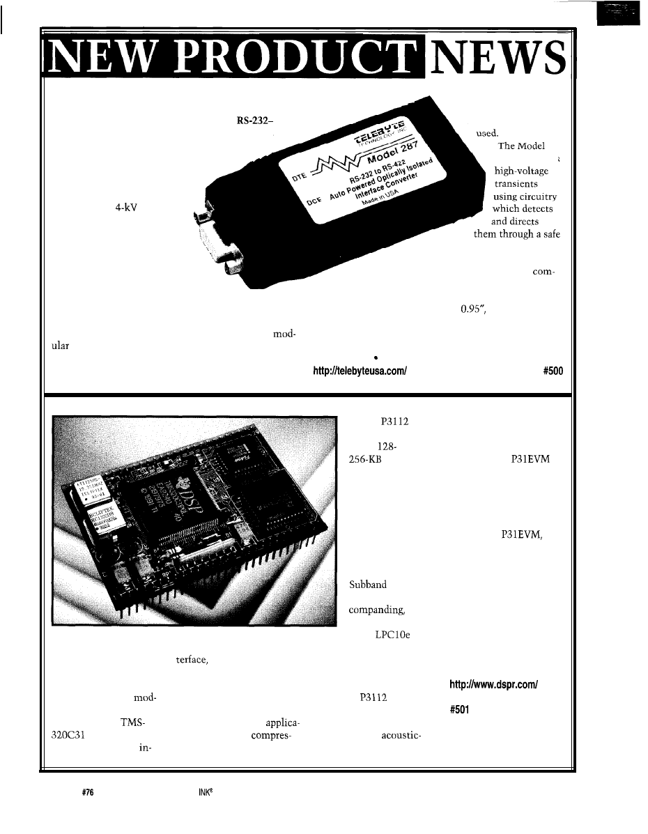
OPTICALLY ISOLATED INTERFACE CONVERTER
The Model 287 miniature Optoisolated
RS-422 Interface Converter
extracts its power from
the
RS-232
interface. The power is further
conditioned to provide an isolated
power supply which operates the
link side of the interface con-
verter. Its isolation capabil-
ity withstands
surges.
link cable if one is
287 withstands
The Model 287 includes
a DE-9 female connector, so
it can attach directly to any
path to ground. The path
PC COM port. A DTE/DCE
includes a ground stud to which is
switch can reverse the transmit
affixed a 12” ground-wire connection
and receive data signals when the
posed of a 16-AWG wire with lug terminals.
Model 287 interfaces to a different type of
The Model 287, which is housed in a small plastic
port. The control signals are also used as a power source.
container measuring 3.3” x 1.7” x
sells for $155.
Data is accommodated at rates up to 19.2 kbps.
The link interface is complemented in an RJ-12
Telebyte Technology, Inc.
connector. The transmit and receive data signals use
270 Pulaski Rd.
l
Greenlawn, NY 11740
the four inner pins of the RJ-12 connector, while the two
(516) 423-3232 Fax: (516) 385-8184
outside pins are reserved for grounding a shield on the
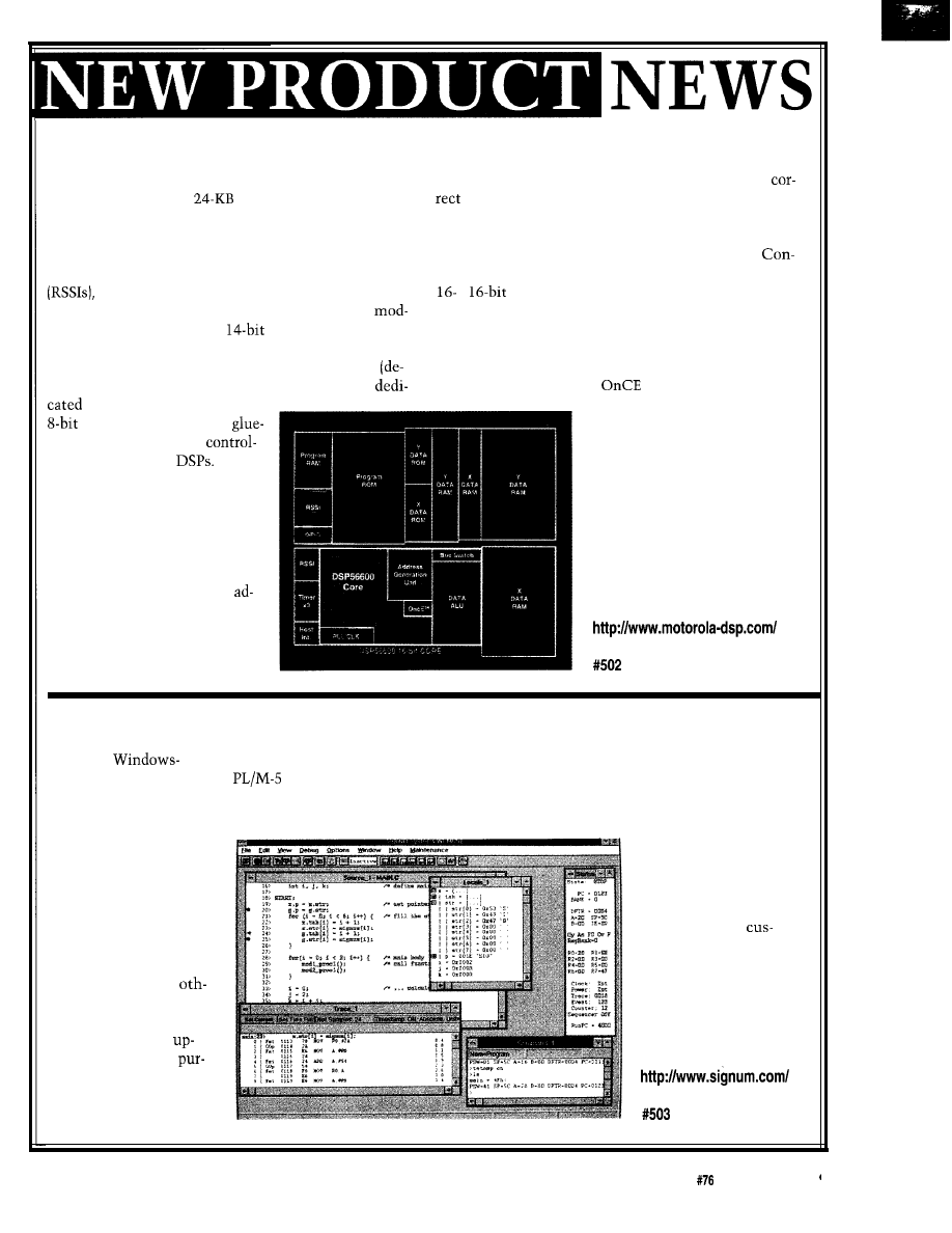
SPEECH-CODING SUBSYSTEM
The Piranha from DSP
on-module A/D-
Research is a complete
D/A conversion with filters,
speech-coding subsystem
an externally clocked serial
on a single plug-in
interface, and 512 KB of
ule. The P3112 is driven
zero-wait-state SRAM. The
at 60 MHz by a
unit is ideal for DSP
processor. It has
tions like speech
a full-duplex analog
sion and fax/modems.
The
stores
user programs in a
single
or
EPROM.
For voice-processing
applications, DSP
Research supplies a
large library of
ready-to-run algo-
rithms, including
ITU 6.728 Low
Delay CELP, G.726
ADPCM, G.722
ADPCM,
6.711 p-/A-law
USFS
CELP 1016, and
USFS
1015.
Algorithms can be selected
by changing the serial clock
rate or by setting mode bits.
The speed and SRAM size
enable the
to support
MIPS- and RAM-intensive
applications such as mo-
dems, line- and
echo cancellation, and very
low bit-rate voice com-
pression.
You can evaluate the
P3112 via the
evaluation platform us-
ing speech input from a
taped source or telephone
handset. Individual
P3 112 modules cost
$1250. The
which comes with a
single P3 112 module
installed, is priced at
$1995.
DSP Research, Inc.
1095 E. Duane Ave.,
Ste. 203
Sunnyvale, CA 94086
(408) 773-l 042
Fax: (408) 736-3451
8
Issue
November 1996
Circuit Cellar
DSP FEATURES LOW POWER AND HIGH SPEED
The Motorola DSP56602 delivers 60 MIPS at 60 MHz
predefined location in on-chip RAM containing the
and 2.7 V. It features a
program ROM along with
or enhanced code replaces the compared instruction.
12 KB of data ROM divided between x and y memories.
The DSP56602 offers a highly parallel instruction set
For RAM, the DSP56602 includes 4 KB each of x and y
which controls the Arithmetic Logic Unit (ALU), the
RAM and 5 12 words of program RAM.
Address Generation Unit (AGU), and the Program
It uses two Reduced Synchronous Serial Interfaces
trol Unit (PCU). The data ALU features a fully pipelined
which offer high-speed serial links to analog
x
parallel multiply accumulator with a 40-bit
converters with different data rates. A triple timer
parallel barrel shifter for single clock-cycle throughput.
ule composed of a common
prescaler and three
It also includes a phase-locked loop that enables the
identical 16-bit timers is also provided. In addition, there
core to run at full speed from low-frequency, off-chip
are 3-3 1 general-purpose I/O (GPIO) lines available
clock sources, even though they are at a much lower
pending on the peripherals enabled) and 3 external
frequency. The enhanced
module lets developers
interrupt lines. An HI08
examine and modify all internal
host interface provides
resources in real time, reducing
less connection to other
software-development efforts.
lers, processors, and
The DSP56602 costs less than
The DSP56602 offers on-chip
$20 in quantity.
program ROM patching. Service
providers can correct or enhance
Motorola DSP Division
software without returning the
MS 0E314
product to the manufacturer. The
6501 William Cannon Dr. W
patch logic consists of four patch
Austin, TX 78735-8598
address registers. Writing an
(512) 891-2000
dress to one of these registers
Fax: (512) 891-3877
starts a c omp a r e each time a new
instruction is fetched from inter-
nal program ROM. A j
ump to a
8051 DEVELOPMENT ENVIRONMENT
Signum Systems has
95, and Windows NT. It
ging and verification tools
ESDS-5 1 features a
released a
supports all major C- and
(e.g., variable quick watch,
cycle-level simulator for
based version of its devel-
1 compilers at the
pass-points, performance
debugging without an
opment environment.
source level with the latest
analysis, coverage analysis,
emulator. It also supports
The Embedded Systems
advanced software debug-
and register breakpoints).
remote debugging via IP
Development Studio
networks. Remote debug-
ESDS-51 operates with
ging enables an ESDS-5 1
the USP-5 1 emulator, a
session to be accessed
state-of-the-art in-circuit
over the network using a
emulator that supports
standard telnet client for
most popular 805 1 -based
co-debugging or
microcontrollers from
tomer support.
Intel, Philips, Dallas
Semiconductor, and
Signum Systems
ers. ESDS-51 is available
11992 Challenger Ct.
bundled with the USP-5 1
Moorpark, CA 93021
emulator and as an
(805) 523-9774
grade for previously
Fax: (805) 523-9776
chased systems.
ESDS-5 1 runs under
Windows 3.1, Windows
Circuit Cellar INK@
Issue
November 1996
DUAL
INTERFACE
The AVT-715 is a dual
interface that enables a
PC to connect to and communicate with a
bus-
equipped automobile. The SAE
is a two-part stan-
dard for an in-vehicle multiplex bus that enables various
sensors, actuators, and controllers to communicate.
Additionally, external test equipment can access the bus
for diagnostics and other maintenance purposes.
The AVT-715 provides both a Variable Pulse Width
(average bit rate = 10.4 kbps) and Pulse Width Modula-
tion (average bit rate = 41.6 kbps) interface on one board.
Functionally, the AVT-715 acts as a protocol translator
and message buffer between a controlling PC and the
bus. Communications between the AVT-715 and
the PC is via an RS-232 or RS-422 serial link (jumper
selected). The serial data rate is jumper selected among
four baud rates (9.6, 19.2, 38.4, and 57.6 kbps).
The AVT-715 is offered as a ready-to-use package for
$1200 or as an OEM module for $800. The ready-to-use
package includes the AVT-715 dual
interface board
housed in a NEMA 4X enclosure, a serial interface cable,
an OBD-II cable assembly, Windows
controller
software, and a user manual. The OEM module consists
of the board and user manual with programmer’s infor-
mation.
Advanced Vehicle Technologies, Inc.
1509 Manor View Rd.
l
Davidsonville, MD 21035
(410) 798-4038
l
Fax: (410) 798-4308
or
only
60
at 9 V
bit-programmable, digital, bits
level
OR
S
ENIOR
MICROMINT, INC.
4 Park Street
l
Vernon, CT 06066
l
Tel: (860) 871-6170
l
Fax: (860) 872-2204
l
in Europe: (44) 1285-658122
l
in Canada: (514) 336-9426
l
WELCOME!
Issue
November 1996
Circuit Cellar INK@
RS-232 TRANSCEIVER
The MAX3237
RS-232 output levels for
3
and 1000
the MAX-
ables the MAX3237 to
speed data transceiver is
data rates to 1 Mbps and
3237’s guaranteed data rate
monitor modems and
ideal for fast modem
above. The charge pumps
(250 kbps) makes it
other external devices
applications. Dual
require only four small
ible with PC-to-PC
without the danger of
nal charge pumps and a
external capacitors.
nication software such as
heavy current (in the
proprietary, low-dropout
normal operating mode
In its megabaud
event that
to an
output stage ensure true
with a worst-case load of
mode (MBAUD = v,.) with
external device is turned
a maximum load of 3
in
off) resulting from
parallel with 250
the
ward bias on a protection
guaranteed data rate is
diode in that device.
1000 Mbps with guaranteed
The MAX3237 comes
slew rates of 24
in a
SSOP and
The MAX3237 contains
costs $3.29 in quantity.
five drivers and three receiv-
ers, providing a complete
Maxim Integrated Products
serial port for notebook,
120 San Gabriel Dr.
subnotebook, and palmtop
Sunnyvale, CA 94086
computers. For modem
(408) 737-7600
support, it offers a
Fax: (408) 737-7194
shutdown mode in which
all three receivers remain
active. This capability
Advanced Vehicle Technologies
multiplex bus products support
the design and testing
network
components.
.
Bus
VPW, PWM,
. Analog
Hardware
. Embedded
Development
. PC
Development
. Hardware Software
Integration
n
Prototype
Hardware Development,
Assembly, and Test
Advanced Vehicle Technologies, Inc.
l
Easy to use schematic entry program
for circuit diagrams,
only $149. Includes netlisting, bill of materials, extensive parts libraries.
l
Powerful, event-driven digital simulator
allows you to check
logic circuitry quickly before actually wiring it up. Works directly within
the
editor from a
menu and displays results in “logic
analyzer” display window. Starting at $149 this is the lowest cost
simulator on the market. Library parts include TTL, and CMOS devices.
l
Analog simulator
for $149. Allows AC, DC and transient
circuit analysis. Includes models of transistors,
and op amps.
l
Circuit board artwork editor and autorouter programs
starting at $149. Produce high quality artwork directly on dot matrix or
laser printers. You can do boards up to 16 layers including surface mount.
Includes Gerber and Excellon file output. Autorouter accepts
and
placement data directly from the
schematic editor.
l
Low cost combination packages with schematics and PCB design:
for
for $649.
Write or
demo disks:
MENTAL AUTOMATION.,.
5415 136th Place S.E.
WA 98006
(206) 641-2141
l
BBS
641-2846
Internet:
Circuit Cellar INK@
Issue
November 1996
1 1
A/D ADAPTER
ADNAV Electronics has
based data-acquisition applications
the
a
that require ultimate portability
low-cost 12-bit A/D adapter for the
and flexibility.
PC parallel printer port. The
comes with
ter is a simple and convenient
software utilities that enable
for acquiring analog signals
time display of acquired
directly on a PC at rates of up to
forms and ASCII-format data
7500 samples per second.
logging to disk, as well as
conditioning information is
resolution spectral analysis of
plied, making it easy to collect data
acquired data. The source code
from analog-output instruments,
C, and assembly) for these
sensors,
loops, and many other analog sources.
utilities is included at no extra cost. Software drivers,
Power for the unit is derived directly from the PC’s
Visual Basic
and programming examples are also
printer port. The micropower design of the adapter’s
provided. The adapter sells for $59.
internal circuitry ensures that it can be used with virtu-
ally any desktop, laptop, or notebook PC. The adapter’s
ADNAV Electronics
design, in conjunction with its small size-a shielded
58 Chicory Ct.
l
Lake Jackson, TX 77566
case
measuring 2” x 2.4“ x
it ideal for
(409) 292-0988
l
Fax: (409) 292-0988
PC BUS MOTION CONTROLLER
The Model 5643 Intel-
ligent
(IP)
Carrier Board,
featuring a
TI
CPU running
ROM-DOS, lets you
develop motion-control
and other applications
using standard PC-based
development tools.
based motion processors
can be added in a modu-
lar fashion to the board.
Acting as a coproces-
sor on the EISA bus, the
5643 ensures that real-
time control functions
are not degraded by the
host CPU overhead or
operating-system limita-
tions. Hence, systems
using a Windows-based
GUI can reliably offload
machine-control func-
tions to the 5643, which
operates independently
from host-PC activities.
The 5643 features
32-KB battery-backed
static RAM for
defined parameter storage
and
dual-port RAM
for fast communication
with the host PC. It has a 2-,
or 6-MB DRAM configu-
ration for running large
programs and an optional
2 MB of flash memory for
additional program storage.
Also available are 48
programmable DIO and an
optional math coprocessor
for applications that de-
mand floating-point calcula-
tions. Dual serial ports
(RS-232 and RS-232/-485)
provide fast communica-
tions with external systems.
The board has sockets for
four single- or two
wide IP modules which can
be I/O or
memory
mapped. The
5643 was
created for up
to 8 axes of
servo and/or
stepper mo-
tion control.
The board’s
modular design allows ADC
and DAC control, encoder
interfacing, and other func-
tions to be incorporated
with motion control. A
interface offers
additional expansion capa-
bilities.
Standard power and util-
ity connectors give the 5643
stand-alone capabilities. A
keyboard is easily imple-
mented in the
utility
interface.
The board’s software
library is compatible with
most C, C++, Visual Basic,
Visual C++, and Turbo Pas-
cal compilers, and it in-
cludes Windows
Tech
80’s
Modular Motion
toolkit lets designers
easily incorporate IP
modules onto the 5643
using a Windows-based
interface. Pricing for the
Model 5643 begins at
$1450. Also available is
the 5643 Development
Kit for easy implementa-
tion in development and
prototype stages.
Technology 80, Inc.
685 Mendelssohn Ave. N
Minneapolis, MN 55427
(612) 542-9545
Fax: (612) 542-9785
12
Issue
November 1996
Circuit Cellar
FEATURES
Building a
Performance DSP System
Bob Fine
Real-Time DSP Modems
with a PC and Sound Card
Building a High-Performance
DSP System
Algorithms and Software
for
Modems
Empowered Digital
Filtering
Winners of the 8th Annual
Circuit Cellar
Design Contest
Self-Tuning PD Algorithm
for the
Getting Started with
Xilinx
The Thrifty Engineer
SP technology is
tools increases and costs come down.
As designers become more aware of
DSP performance benefits, they’re
creating new ways of implementing
DSP in their systems.
For those not familiar with some of
the DSP devices on the market, I’d like
to introduce you to Analog Device’s
ADSP-2100 family of
1’11 look at
the
architecture, walk
through a system-design example, and
discuss issues relating to both hard-
ware and software development.
You should get enough information
to get started on a DSP system design.
FAMILY ARCHITECTURE
All
DSP chips share a
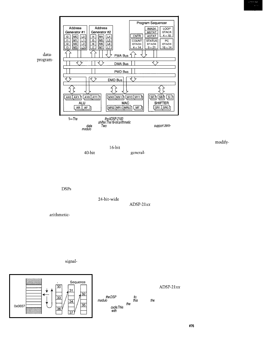
common base architecture. As shown
in Figure 1, this architecture consists
of arithmetic, address-generation, and
program-sequencer sections.
The architecture is rich with regis-
ters and flexible in performing calcula-
tions and moving data. The internal
bus structure also provides flexibility
in data and instruction handling.
Several features of DSP architecture
set it apart from conventional micro-
processor or RISC architecture. Most
notably, DSP performs fast,
1 4
Issue
November 1996
Circuit Cellar INK@
cycle
arithmetic opera-
tions. To ensure that the
processor sustains these
calculations every cycle,
the required data oper-
ands are fetched every
cycle.
The arithmetic,
addressing, and
sequencing sections of
the ADSP-2100 base
architecture are intercon-
nected via a modified
Harvard architecture bus
structure.
A modified Harvard
architecture supports an
instruction fetch from
program memory in the
same cycle as two data
fetches take place-one
from data memory and
the other from program
memory. The ability to
Figure
base architecture for
family consists of an arithmetic section
containing an ALU, MAC, and
units a/so perform multiprecision
operafions for larger
words.
independent data-address generafors
overhead circular
addressing, and a program sequencer supports zero-overhead
nested looping.
fetch two data words and one instruc-
tion in a single cycle is critical for
efficient implementation of DSP algo-
rithms.
ARITHMETIC SECTION
Like a digital filter, many DSP algo-
rithms have arithmetic operations
performed with data and coefficient
values. The key advantage of
over other micros is the ability to
perform arithmetic operations in a
single cycle.
Responding to interrupts in real
time also involves the
section architecture. If the arithmetic
unit is used in the interrupt service
routine, the data used in the main
routine needs to be saved so it can be
restored after the interrupt is serviced.
This technique is called a context
save and restore. A DSP with an auto-
matic context-switching mechanism is
the most efficient for real-time
processing applications.
The arithmetic section consists of a
16-bit ALU, a
MAC with a
accumulator, and a
purpose shifter. Each arithmetic unit
has a number of input and output
registers, interconnected by the bus
structure, which consists of data-mem-
ory, program-memory, and result bus-
es. Through this bus structure, two
operands can be fed to the arithmetic
units in a single cycle.
The
instruction and
the instruction set of the
processors allow a high level of paral-
lelism. Many operations occur in one
cycle, yielding a high MOPS rating.
DATA ADDRESSING
DSP algorithms require two oper-
ands fetched from memory in a single
cycle to be subsequently fed to the
arithmetic units. To supply the ad-
dresses of these two operands in a
flexible manner, two address genera-
tors are required.
0x0030
n
Address
Figure 2-Jhe data-address generators
within
must be able support
circular buffering. In
example,
address is modified by value 3 in each
instruction
modification is
performed
zero overhead so a new
address can be output every cycle.
Given the modified
Harvard architecture,
one address generator
must supply an address
over the data-memory
address bus while the
other supplies an address
over the program-mem-
ory address bus.
DSP algorithms also
require circular buffering
(i.e., data in a buffer is
addressed so the address
pointer wraps from the
end back to the start of
the buffer). Some appli-
cations need to support
circular buffering even
when the pointer ad-
vances by values greater
than one. Figure 2 shows
how this modulo circu-
lar buffering works.
The address-genera-
tion circuitry performs address
and-compare operations in hardware
for optimum efficiency. Performing
these functions in software limits the
processor’s ability to handle real-time
signals.
In Figure 2, a buffer of eight loca-
tions resides in memory starting at
address 30. The address generator cal-
culates the next addresses within the
buffer while keeping the proper data
spacing so two locations are skipped.
The address generator outputs ad-
dress 30 onto the address bus while it
modifies the address to 33 for the next
cycle’s memory access. When address
36 is modified to address 39 (outside
the buffer), the address generator de-
tects that the address is outside the
buffer boundary and modifies the ad-
dress to 3 1. It is therefore connected
back into the start of the buffer.
The update, compare, and modify
occur with no overhead. In one cycle,
address 36 is output onto the address
bus. In the next cycle, address 31 is
output onto the address bus.
The data-addressing section of the
architecture has two ad-
dress generators, each containing four
address (I), four modify (M), and four
length (L) registers.
An address is output to the address
bus by specifying an I register. The
Circuit Cellar INK@
Issue
November 1996
15
address is modified in preparation for
the next operation by the specified M
register. The L register specifies the
length of a circular buffer.
PROGRAM SEQUENCING
The program sequencer must loop
through algorithm code efficiently
without incurring any extra time or
overhead to get from the end to the
start of the loop. This so-called
overhead looping is quite different
from conventional microprocessors.
A typical microprocessor requires
you to maintain program loops in
software. A conditional instruction
placed at the end of the loop deter-
mines whether a j ump directs program
flow back to the top.
With a DSP, the loop’s last instruc-
tion executes in one cycle. In the next
cycle, either the first instruction at the
top or the first one outside the loop is
executed. Of course, hardware support
for nested loops is required, especially
for multidimensional algorithms.
DSP algorithms also involve
world signals converted into digital
Instruction
Program
Data
Rate
Memory
Device
Voltage (MIPS) RAM (words)
Comments
ADSP-2101
03
25
2 serial ports
ADSP-2104
2 serial ports
ADSP-2104L
20
512
2 serial ports
13.8
512
256
ADSP-2105
2 serial ports
20
512
1 serial port
ADSP-2109
256
4 K word ROM, 2 serial ports
3.3
256
4 K word ROM, 2 serial ports
1-K
512 512
2 serial ports
ADSP-2162
8 K word ROM, 2 serial
3.3
K word ROM,
ADSP-2163
512
8
2 serial ports
512
ADSP-2164
4 K word ROM, 2 serial ports
_
512
ADSP-2171
4 K word ROM, 2 serial ports
ADSP-2172
2 serial ports, host port
ADSP-2173
8 K word ROM, 2 serial ports, host
3.3
ADSP-2181
2 serial ports, host
ADSP-2183
2 serial ports, 2 DMA ports
16 K
16 K
2 serial ports, 2
ADSP-2185
DMA ports
33
2 serial ports, DMA
16 K
ADSP-2186
2 serial ports, DMA ports
ADSP-2186L
2 serial ports, DMA ports
ADSP-21 msp58
2 serial ports, DMA ports
2 K
host port, analog
26
4 K word ROM, host port, analog I/O
Table
l-Analog Devices
has one of the largest code-compatible families of
A single development system
lets you develop code for processors listed, so you can migrate from one
device to
another while preserving
code.
representations by the ADC. The ADC
usually lets the DSP know that a data
sample is ready via a hardware inter-
rupt. Since interrupts need to be han-
dled in real time in a DSP application,
the DSP must respond to interrupts
quickly and efficiently.
40;
Your Choice
for
C Compilers
Byte Craft’s optimizing C compilers are fast
and efficient. C extensions provide control
over bit manipulations, I/O port and memory
definitions, as well as support for direct
register access and interrupts.
We respond to your C compiler needs.
Byte Craft
421 King Street N., Waterloo, Ontario CANADA
Tel:
(519) 888-6911 Fax: (519) 746-6751
BBS: (519) 888-7626
MELPS740
COP8
The
program sequencer
determines the next instruction to be
fetched from program memory. It sup-
ports nested and zero-overhead loops,
multiple stacks, and low-latency inter-
rupt responses. Many sequencing func-
tions are performed in the hardware
rather than in the software.
ASSEMBLY-LANGUAGE SYNTAX
The assembly-language syntax of
the ADSP-2100 family is algebraic
rather than mnemonic. As you can see,
an arithmetic operation and two data
fetches are specified in a single in-
struction for single-cycle execution:
MR = MR + MXO MY1
MXO =
MY1 =
The first clause instructs the processor
to multiply the data in register MXO
with the data in register MY 1. This
product is added to the contents of the
multiplier result register, MR, and
stored as the new contents of MR.
The second clause instructs the pro-
cessor to fetch data from data memory
using the contents of the register IO as
the address. While data is being fetched
and stored in register MXO, the address is
modified by the contents of register M2
and reloaded into IO. If length register LO
was loaded with a
value, the
update is performed, keeping the address
value within a circular buffer.
16
Issue
November 1996
Circuit Cellar
ADSP-2100 Base Architecture
ADSP-1281 Integration
Figure 3-The
adds K words ofprogram-memory RAM, 16 K words of data-memory RAM, two serial
capability, a programmable timer, an and
pod, power-down control logic, and
The large amount of on-chip RAM
the need for
external RAM, saving design time,
and board space.
The third clause, like the second
clause, loads the register MY1 with a
value from program memory while
updating the address pointer IS.
are used) to understand what the sys-
tem looks like and flag errors. After
the code is debugged, the PROM split-
ter formats the DSP code for download
to a PROM programmer.
ADSP-2100 FAMILY
The ADSP-2100 family starts with
low-cost devices under and contin-
ues up to high-performance, highly
integrated devices. The members differ
in memory and peripheral configura-
tions.
Analog Devices’ software develop-
ment package supports all fixed-point
processors. It contains the assembler,
system builder, linker, simulator,
PROM splitter, a C compiler and
source-level debugger, C
li-
brary, and librarian.
In some cases, different members
Once the DSP program is loaded
have identical
so a hardware
onto the processor and the hardware is
upgrade can be performed by plugging
running, EZ-ICE can provide
a new DSP into the existing socket.
sive target-based debugging. It uses a
This feature provides a low-cost entry
wide range of functions, including
point with an upgrade path leading to
single-step and full-speed execution
higher performance, larger memory,
with predefined breakpoints, and it can
and more peripherals without changes
view and change contents of the pro-
to the circuit board.
cessor’s registers and memory.
Table
1
summarizes the ADSP-2 lxx
devices and their key features. All
devices have a
timer with a
prescaler, boot address generator for
automatic booting from an external
EPROM at
with no glue logic,
and an external parallel port.
EZ-Lab evaluation boards have small,
low-cost controls (e.g., push buttons and
indicator lights) and an EPROM socket
for stand-alone operation.
ADSP-2181
DEVELOPMENT TOOLS
Simulators let you profile the code’s
performance, plot digital signals on the
screen, simulate I/O capabilities, and
set complex breakpoints. A system
builder creates a description of the
hardware system (e.g., how much
memory and what extra components
The ADSP-218 1 offers the highest
level of integration available in a
fixed-point DSP. It contains
16 K x 16 words of data memory and
another 16 K x 24 words of program
memory for instruction and data stor-
age.
Data-memory addressing is con-
trolled by two programmable address
generators. The address generators can
O w n
V i r t u a l W o r l d s
a n d S h a r e T h e m w i t h
M i l l i o n
Learn How to Build Your Own Virtual Reality
Worlds Quickly and Easily!
0 Explore your
Worlds on Your PC or put
them on the Internet for Others to Explore!
Explore your Worlds with your PC monitor and
keyboard, or with Greaterlmmersion using
VR
with head
cost
$4000
a
ago.
Now
they under
And 3-O VR Shutter
Glasses are under
Now
affordable
on
love it! At under
book, don’t miss
out on this Incredible Value!”
-Pam -
-
PC, plus:
(head mounted displays) other equip The
Mattel
hack
a $39
sources
of virtual world building-software
l
Comprehensive
of HMD
games
l
Plus much more!
l
36 pp.
Primer
explains VRML
Modeling Language”), plus: Building virtual
on the Internet
virtual
on the Internet
l
More!
l
32 pp.
Virtual
an
Exclusive
on
News
weights Fortune
l
The VR marketplace
l
28 pp.
valuable
induding Listings of Internet
devoted to
papers
l
Listings of Internet
download sites VR-related newsgroups
l
Article
listings from back issues of VR magazines
l
Where
to go to experience real VR
l
Reviews of popular VR
books
l
Glossary of VR terms
l
Great VR applications
l
pp
is yourguide
involved
VR
software.
R&D
plus professional bade organize
dubs, more! 80 pp. Yours absolutely FREE!
VR
Cartoons
featuring dozens of funny
cartoons about VR! Yours absolutely FREE!
Limited printing, don’t
out! Order today!
Circuit Cellar INK@
Issue
November
1996
point to data words in data memory as
well as program memory.
A program sequencer controls in-
struction execution and maintains the
address for instructions in the program
memory. The ADSP-2181’s arithmetic
section consists of a MAC, an ALU,
and a shifter. Two serial ports, an in-
terval timer, and interface circuitry
complete the ADSP-2181’s architec-
ture shown in Figure 3.
With a highly integrated DSP, the
memory subsystem is built in, result-
ing in improved data flow.
can
only access external memory once per
cycle because they typically have a
single external bus.
The ADSP-2 18 1 performs three
internal memory accesses each cycle.
program is running. When the transfer
is complete, the processor’s internal
circuitry generates an interrupt to let
the program know that the memory
transfer has taken place.
SYSTEM CONSIDERATIONS
Do you need complex algorithms
requiring high computational through-
put from the DSP! Are you designing
battery-powered equipment or a sys-
tem that has low power consumption?
The benefits of large memory and
the variety of DMA features are fur-
ther enhanced by a
instruc-
tion rate, an enhanced instruction set,
and low-power modes.
The instruction rate deserves a
closer look because rates alone do not
G.721 Wide-Band ADPCM
G.728 LD-CELP
26.8 &sample
GSM Speech Coding
Half-Rate
Speech Coding
1.975
13 ms
IS-54 VSELP Speech Coding
9.78 ms
Complex FFT
1.07 ms
Complex FFT
5.5 ms
Full-Duplex Speaker Phone
9.5 MIPS
modem
15 MIPS
modem
28 MIPS
Table
its
multi-
function instructions,
performs many
operations in a sing/e instruction cycle.
This feature
the
to
execute sophisticated
algorithms in
fewer
fhan other
In 30 ns, the next instruction can be
indicate a processor’s performance. It’s
fetched while one data word is fetched
better to look at how many operations
from data memory and another from
can be performed in a single cycle.
program memory.
In a single cycle, the ADSP-218 1 can:
The ADSP-2 18 1 is a register-based
processor with registers surrounding
the
and outputs of all the arith-
metic units. These registers further
enhance the processor’s ability to effi-
ciently move and store data.
l
fetch a data word from data memory
l
calculate the next address for data
memory with a user-specified value
l
fetch a second data word from pro-
gram memory
The large internal memory and effi-
cient architecture of the ADSP-2181
translate into performance not possible
on other fixed-point processors. The best
example is the
FFT which
executes on the ADSP-2181 in 5.5 ms
with no external memory.
l
calculate the next address for pro-
gram memory with a user-specified
value
ACCESSIBLE MEMORY?
l
detect the passing of a circular buffer
boundary and automatically correct
the memory pointer for both data
and program memories
l
fetch the next instruction from pro-
gram memory
But, on-chip memory doesn’t solve
anything unless it’s accessible. The
ADSP-2181 has several ways to di-
rectly access the memory-serial port
DMA, byte memory DMA (BDMA),
and internal memory DMA
These DMA channels allow data to
be transferred in and out of the
218 l’s internal memory while your
l
detect the termination of an instruc-
tion loop and automatically adjust
the program counter to either the
start of the loop or outside the loop
l
perform an arithmetic calculation
with user-specified source registers
l
store the result of the arithmetic
operation into a specified destina-
tion register
l
update the timer
l
receive and transmit data through
the two serial ports
This cycle runs every 30 ns at the
MHz rate.
This code for the core loop of an FIR
filter illustrates the high degree of
parallelism in the instruction set:
DO TAP-LOOP UNTIL CE
TAP-LOOP: MR=MR+
The value in register MXO is multi-
plied by the value in register
This product is added to the
register contents and stored as the new
contents of the result register.
The registers MXO and MY are
also loaded from the data memory and
program memory, respectively. The
address pointers IO and 14 are modified
by the values in registers M2 and M5,
respectively. At the same time, the
next instruction in program memory is
fetched and decoded.
The external clock only needs to be
half the instruction rate. To run the
processor at 33 MHz, connect it to a
crystal or oscillator.
Because of the low speed, the crys-
tal oscillator or clock is easier to find
and less expensive to buy. And, you
won’t have to worry as much about
the effects of radiated high-frequency
noise.
Many applications require a DSP
with low power consumption. The
ADSP-218 l’s low-power modes extend
battery life, decrease heat caused by
power-supply-regulator power dissipa-
tion, and decrease radiated noise levels
from high-frequency current surges.
SYSTEM COMPARISON
Using an audio signal-processing
system design, implemented conven-
tional and highly integrated
I’ll
compare the cost, design time, and
performance of the systems.
The following DSP system contains
32 K words of static RAM, a host inter-
face, and a boot ROM. Since the DSP
doesn’t have enough internal RAM,
external RAM is added. The access
time required for these
is 12 ns.
18
Issue
November 1996
Circuit Cellar INK@
Power Connector
AD1 847
Mic/Line
Stereo Analog
Stereo Audio
Signal Selector
Input
Soundport
Stereo Analog
output
Emulator
Connector
ADM232
, R S - 2 3 2
ADSP-2181
Driver
Connector
S o c k e t e d
D S P
EPROM
User Push Buttons
and
Expansion Connectors
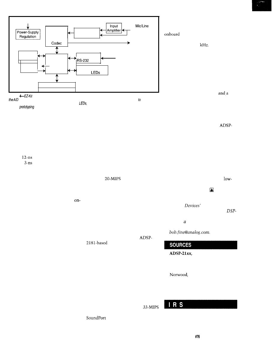
Figure
Life is designed around the ADSP-2181 DSP processor. An AD1847 stereo audio codec provides
and D/A conversion and analog-signal interface. An RS-232 interface connects the kit board a computer
or any system supporting RS-232. User push buttons,
a socketed EPROM, and expansion connectors
simplify
and experimentation.
An address-decoder circuit creates
the various chip-select signals for the
RAM components. The address de-
coder requires -3 ns of propagation
delay from the time the address on the
bus settles to the time the outputs are
valid.
The
access time of the RAM
plus the
address decode time
yields a total access requirement of
15 ns. The host processor connects to
the DSP system bus by an interface
circuit. It can also access the DSP
RAM via the DMA controller circuit.
The DSP system based on the
ADSP-218 1 contains 32 K words of
chip RAM (external memory is unnec-
essary). Since the complete memory
system is on-chip, an address decode
circuit or timing analysis isn’t re-
quired.
The host connects to the DMA port
of the ADSP-2181 with an interface
circuit.
Since the DMA capabilities of the
ADSP-2181 are used, an external DMA
controller isn’t required. The boot
EPROM connects to the byte DMA
port and combines with byte RAM,
yielding 4 MB of additional memory
space-without extra interface cir-
cuitry.
Depending on the cost of the mem-
ory components, a system using a
highly integrated DSP can cost $20
less. Eliminating the memory sub-
system design and related test and
debug can shave weeks off the develop-
ment schedule.
PERFORMANCE BENCHMARKS
Since processors’ performances vary
drastically-even with the same clock
rate-it’s best to look at benchmarks
of algorithms you’re going to run in
your system and operations per cycle.
Judging a DSP by its clock speed or
instruction rate alone can be mislead-
ing. For example, a processor with a
40-MIPS rating that performs only one
operation per instruction is less power-
ful than a
processor perform-
ing three operations per instruction.
Processor bandwidth benchmarks
are usually specified as a percent load-
ing or a MIPS requirement. So, if a
20-MIPS processor implements a par-
ticular benchmark using 10 MIPS, the
processor is 50% loaded.
It may be possible to run two chan-
nels of an algorithm or implement two
algorithms simultaneously. Table 2
lists the benchmarks for the
systems.
EVALUATION AND DEVELOPMENT
SYSTEM
The ADSP-218 1 is supported by the
low-cost EZ-Kit Lite development
system. It includes the EZ-Lab evalua-
tion and development board and the
software development package (see
Figure 4).
The ADSP-218 1 EZ-Lab provides a
good example of an audio-processing
system. The board features the
ADSP-2181, the AD1847 stereo audio
codec, an RS-232 interface
based on Analog Devices’ ADM 232
chip, and an analog input-signal-condi-
tioning circuit based on the Analog
Devices’ SSM2135 dual op-amp. This
codec provides CD-quality
stereo with a programmable sampling
rate from 5.5 to 48
The board connects to the RS-232
or COM port of a PC. The board can
also be configured to run in stand-
alone mode with programs you’ve
developed.
Once the board is connected to a
power supply, a PC’s COM port, an
analog input source (e.g., microphone,
CD player, tape player, etc.],
set
of powered speakers, you’re ready to
install the software.
STARTING OUT WITH DSP
Building a high-performance DSP
system with a member of the
2100 family gives you a low-cost entry
point to DSP with an upgrade path to
high-performance, highly integrated
processors.
Since all ADSP-2100 family mem-
bers are based on the same core archi-
tecture, they are code compatible. This
means you don’t have to recode your
algorithm when moving from one
processor to another. And, with
cost development tools, it’s easy to get
up and running quickly.
Bob Fine is the product line manager
for Analog
fixed-point DSP
products. He has over 10 years of
system-design experience and has
published number of articles on
DSP-design issues. You may reach Bob
at
EZ-ICE, EZ-Kit Lite,
EZ-Lab, datasheets
Analog Devices
P.O. Box 9106
MA 02062-9106
(617) 329-4700
Fax: (617) 329-1241
http://www.analog.com/
401 Very Useful
402 Moderately Useful
403 Not Useful
Circuit Cellar INK@
Issue
November 1996
19
Digitize32 is an upgrade of the
program in real-time spectral displays
using Windows’ low-level audio func-
tions in INK 61. Most of its Windows
code can be directly compiled with
(16 bit) or
(32 bit).
Matt Park
Brian
Real-Time DSP Modems
with a PC and Sound Card
n “Real-Time
DSP with a PC and
a Windows-compatible
sound card and a ‘486 PC were all that
was needed for real-time DSP.
Building on that article, we offer
examples of real-time DSP-based V.22
QPSK and
QAM modem de-
modulators. We also present some DSP
building blocks you can use.
You might ask-why design some-
thing when you can buy a chip set with
20 times the performance? Because:
l
demodulators are great DSP learning
projects. They incorporate funda-
mental DSP building blocks such as
IIR and FIR filters, down sampling,
frequency mixing and shifting,
adaptive equalizers, feedback loops,
and real-time processing constraints.
l
many DSP building blocks are useful
for embedded systems control
l
as embedded controllers and
merge, you’ll implement data com-
munications directly on the con-
troller, reducing chip count and cost
DIGITIZE32
demodulates
V.22
and
modems
in real
time on a
or faster PC.
We wrote Digitize32 using
for Windows 95 and Windows NT.
Most C++ compilers should compile
the DSP functions and C++ classes.
Ctt OBJECTS
is
good for designing reusable
DSP code. We used it over standard C
because many of the functions (e.g.,
filters, time averagers, and storage
arrays) were used more than once in
the demodulator, and each instance
required its own internal storage.
The C++ class and object concept
enabled us to almost “wire” the ob-
jects together to build a very modular
DSP application.
For example, with the filters in the
demodulator, C++ let us write one filter
class and, in the program, create two
unique instances of that filter class.
But, this isn’t a tutorial on
For
that, see Mike Podanoffsky’s “A C++
Programming Tutorial” (INK 57).
SIGNAL MODULATION
Quadrature Amplitude Modulation
(QAM) uses a digital signal to modu-
late a carrier’s amplitude and phase.
QAM is well-suited for transmitting
digital information over telephone
lines and other high-quality,
limited communications paths. QAM
systems are coherent. They require the
receiver to be phased locked with the
transmitter’s carrier and symbol clock.
QAM systems are called M-ary
QAM,
where M is the number of unique
amplitude and phase combinations.
Two values--l and Q-represent any
M-ary QAM signal because any wave-
form can be expressed as a linear com-
bination of orthogonal phasors.
The numbers of unique amplitude
and phase combinations are called
symbols. When plotted on an
or xy
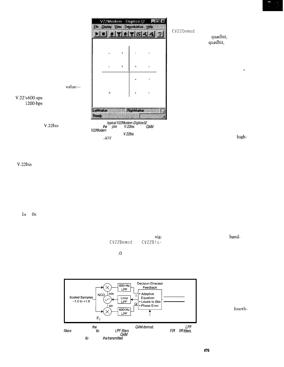
plot, they form constellations. Photo 1
shows the constellation for
Assigning multiple bits per symbol
makes the symbol rate less than the
data rate, reducing the required trans-
mission bandwidth. This reduction is
why we use the more complicated
coherent QAM modulation.
20
Issue
November 1996
Circuit Cellar INK@
The data rate measures how fast the
computer sends bits out of its serial
port (e.g., 1200 bps). The symbol (baud)
rate is the rate that the modem changes
the transmitted waveform (e.g., 600
symbols per second [sps]).
Phase-shift keying (PSK) is a subset
of QAM where the digital signal modu-
lates the carrier’s phase. The CCITT
standard specifies V.22 as a differential
quadrature PSK (DQPSK) signal. For
DQPSK, the phase difference between
two symbols-not the phase
encodes the symbol information.
symbol rate is one
half the
data rate. Each sym-
bol is assigned two bits or a dibit. A 0
degree change is 01, 90 is 00, 180 is 10,
and 270 equals 11.
Both V.22 and
use 1200 Hz
for the low-channel carrier and 2400 Hz
for the high channel. They have simi-
lar frequency spectra and channel
bandwidths. Because they share so
many characteristics, it was easy to
reuse most of the V.22 DSP code for
the
demodulator.
DEMODULATORS
samples of the modulated signal and
uses a quadrature downconverter to
turn them into instantaneous ZQ val-
ues. To demodulator’s performance
can be gauged from ZQ plots which
display ZQ values on a xy graph.
V.22 modems-and most QAM sys-
tems-scramble transmitted data prior
to the transmission modulation to get a
pseudorandom datastream. Random data
gives a constant frequency spectrum and
power density and decreases the num-
ber of or in a row. It’s thus easier
to bit synchronize to the datastream.
Scrambling the data also makes
each symbol equally likely and locates
the optimum symbol-decision thresh-
olds halfway between each symbol.
The bit sync determines when to
sample the instantaneous ZQ values to
make the best estimate of the trans-
mitted bits. And, the descrambler
outputs the correct data bits.
For testing, we used signals from a
pair of standard two-wire modems,
operating in the leased-line mode and
connected directly to each other and
the sound card’s line input. For tele-
phone and other two-wire modems,
both the low- and high-band channels
are present in the audio signal.
A DEMODULATOR IN Ctt
All demodulators must input an ana-
log signal and output the best estimate
of the received bits. Demodulators con-
tain signal-to-levels, levels-to-bits, and
bit-synchronizer (bit-sync) blocks as seen
in Figure 1.
We designed our code to be modu-
lar, work with data from several digi-
tizers, run on different platforms and
compilers, and take higher speed
nals.The
and
Demod classes accept single samples
scaled from -1 to + 1 .O and output the
demodulated bits once per symbol.
The class is constructed with specific
signal and demodulator information such
It isn’t necessary to band-pass filter
the V.22 signals before the demodula-
tor. Mixing with the appropriate car-
rier places the undesired channel’s
signal outside the pass band of the
mixer’s low-pass filters.
By changing the carrier frequency,
the identical DSP code demodulates
either channel. However, not
pass filtering requires a higher order
LPF, which means more time-consum-
ing multiplies per second.
We implemented both FIR and IIR
filters. Linear phase response is impor-
tant for QAM signals. Designs some-
times use FIR filters
QAM modems also
have carrier-tracking and
descrambler blocks.
Newer high-speed QAM
telephone modems need
adaptive equalizers to
correct phase and ampli-
tude distortions in the
transmission path.
The signal-to-levels
block accepts digitized
Descrambler
=
1200
Hz,
2400
H z
Bit Sync
Figure l--These are basic building blocks of any
The NCO, mixers, and
convert the signal levels. The
can be implemented as either
or
Adaptive equalizers are optional for some
demods. The external bit-sync signal triggers
signal sampling determine
data symbol.
l
Photo 1-A
window
displays IQ
for a
X-point
signal.
enables you to demodulate and display
data from live V.22 and
modem signals or
sampled
files.
as
sample and symbol rates, bandwidth,
gains, and feedback-loop coefficients.
outputs an integer value
equal to the dibit or
the string
value of the dibit or
or the ASCII
value of the transmitted character.
It’s handy to have all the demodula-
tor code in one class that can be called
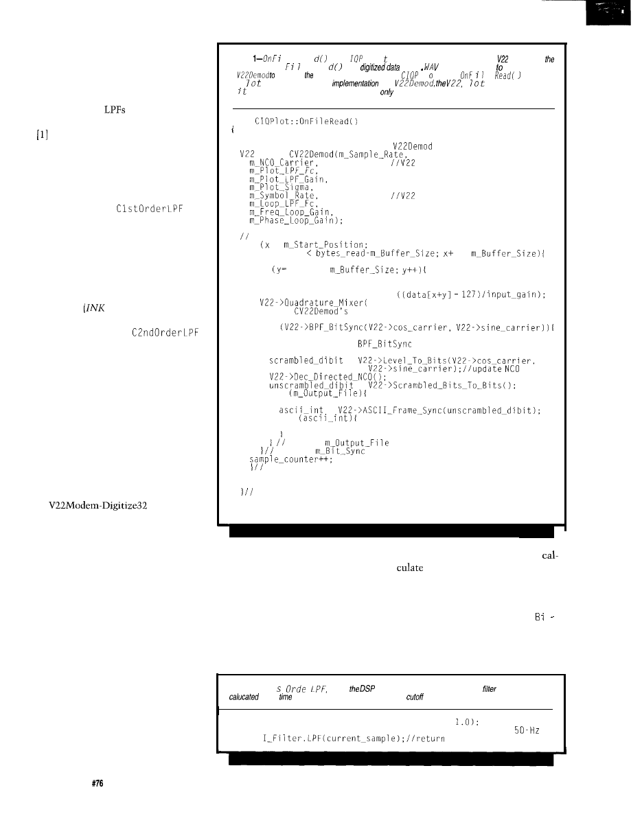
by a real-time or file-based routine.
Listing 1 shows how to use the CV 22
Demod class from a file-based routine.
SIGNAL TO LEVELS
The quadrature downconverter or
mixer operates on each sample and
converts the audio signal from a re-
ceiver or phone line into Z and Q sig-
nals. The frequency mixer multiplies
the current incoming sample by the
carrier numerically controlled oscilla-
tor’s (NCO) sine and cosine values.
The low-pass filters filter out the
frequency terms the mixers produce.
because of their better
linear phase response
and the ease of match-
ing the LPF to the de
sired transmission filter.
We first used
order IIR filters since
they provided high
attenuation for fewer
multiplies and were
easier to implement
Circuit Cellar INK@
Issue
November 1996
21
than FIR filters. This choice originally
meant faster real-time performance
and less time writing code.
We determined the necessary degree
of the filter by trying second-, fourth-,
and sixth-order
designed by using
the Interactive Filter Design Web Page
and looking at the quality of the IQ
plots. However, these predesigned
filter coefficients were only valid at a
single-sample rate.
Since we wanted to experiment
with different sampling rates at run
time, we designed
and
C 2
n d 0 r d e r L P F
low-pass-filter classes.
These classes calculate the IIR-filter
coefficients based on a specified sample
rate and cutoff frequency at program
run time (see Listing 2).
We used equations and procedures
from Do-While Jones’ “Digital Filter
Alchemy”
61)
to
design filter
classes for fast real-time applications.
We
first cascaded two
filters to make a fourth-order filter for
each arm of the quadrature mixer (see
Listing 3).
We used FIR filters to improve the
demodulator’s performance by design-
ing a LPF that better matched the im-
pulse response of the transmission filter
and channel. Because FIR filters require
many more multiplies than equivalent
IIR filters, we oversampled I and Q
signals and downsampled (decimated)
the signals to reduce the time needed
for the FIR filter.
samples the
analog signal using the sound card at a
standard rate of 11,025 Hz. Therefore,
the
I
and Q signals are oversampled at
over 18 samples per signal.
The follow-on equalizer only re-
quires two samples per symbol. So, by
decimating the
I
and Q signals, we
saved significant processing time for
improved real-time performance.
Typically, to eliminate aliasing, a
LPF band limits a signal before deci-
mation. The antialiasing filter operates
on each sample at the higher sample
rate and uses a lot of processing time.
But, a FIR filter can combine filter
and decimate functions because its out-
put only depends on the samples in the
filter at the output time. Every sample is
shifted into the filter, but output calcu-
lations are only performed on 2 of every
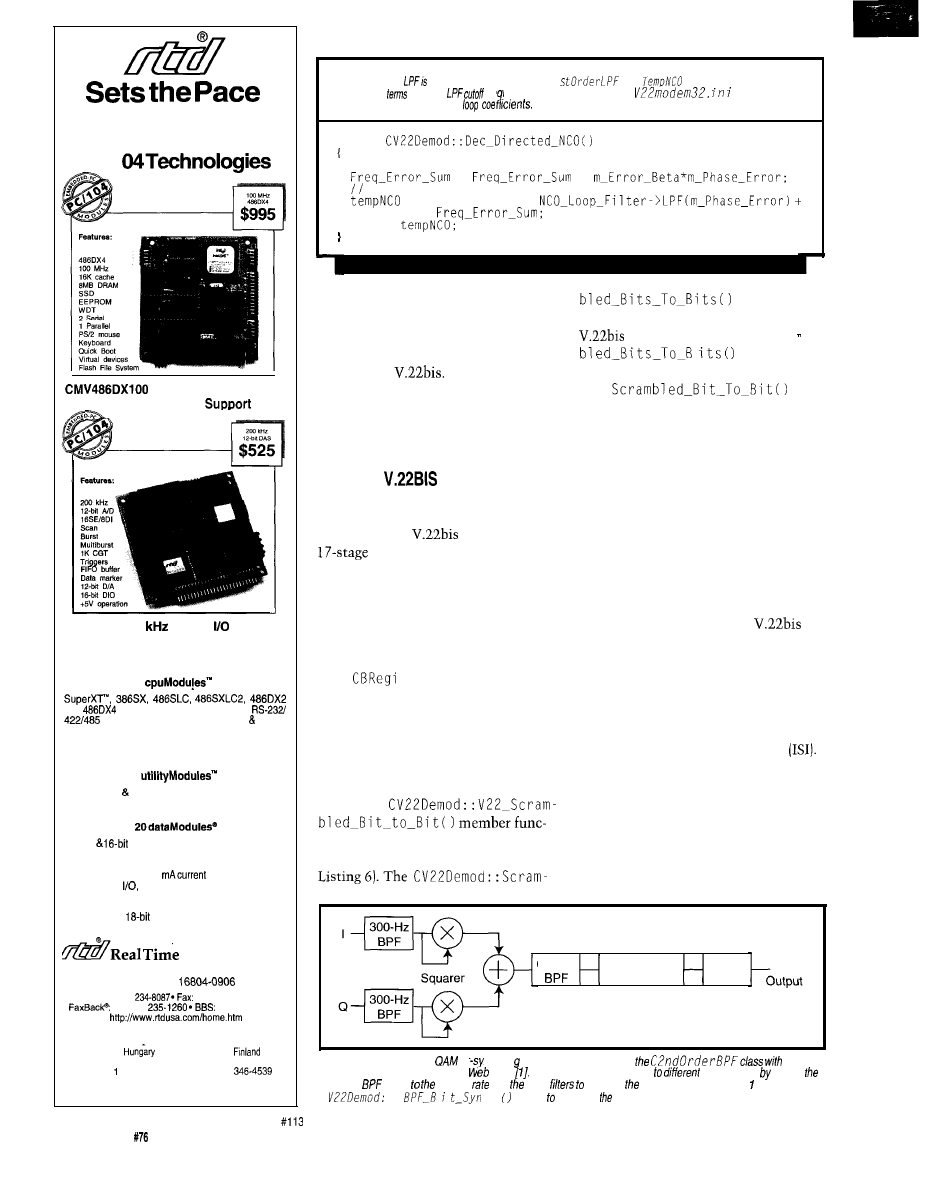
Listing
7 e Rea is the C
7 o member function associated with the
Demod from
file dialog box. On
e Re a reads
from a
file and shows how use
C
implement V.22 demodulator. The complete
7 t : :
e
is in
i qp
. cpp. For a real-time
of C
P
P
O
in t, and
B
Syn c P
O
i n t pointers should be global and
created and deleted when the modem is started and
stopped.
void
(read data buffer from data file)
//construct an instance of the
class
= new
= 1200 or 2400 Hz
//needed for mixer low-pass filter
//needed for mixer low-pass filter
//needed for mixer low-pass filter
= 600 sps
//needed for carrier-tracking loop
//needed for carriertracking loop
//needed for carrier-tracking loop
main loop to process data in buffer
for =
x
=
for
0: y <
//model the real-time buffers received from sound card
//calculated once per sample
double tempdata = (double)
tempdata);
//call
quadrature mixer function
(fill a point array for plotting to screen)
if
//check if bit sync has fired
//all code inside
loop runs once per symbol
=
freq.
//for carrier tracking
=
if
//if output to file is chosen
=
if
(output the ascii character to screen or file)
end of
end of
end of buffer read
//sample number processed
(option to display IO point array)
(option to display bitsynced symbol assignment)
end of data file
18
samples for an effective IQ sampling
It took about the same time to
rate of 1200 Hz or 2 samples per symbol.
the IIR and decimating FIR
For oversampled signals, using a
filters. In the end, the overall demodu
decimating FIR filter helps to increase
lator design drove the choice of using
system performance when using a FIR
an IIR or FIR filter.
filter. If we didn’t implement this
The equalizer design in C
V 2
2 s
function, the 39 tap FIR filters would
Demod
uses two samples per symbol
take too many multiplies and adds to
for the symbol-to-bit, carrier-tracking,
run in real time on a ‘486.
and bit-sync functions, so it uses the
Listing 2-/n Cl t
r
one of
building blocks for this project, the
coefficients are
at run
based on a specified sample rate and
frequency.
ClstOrderLPF I-Filter = ClstOrder(11025.50.0,
//construct a 1 pole,
LPF
temp =
a filtered value
22
Issue
November 1996
Circuit Cellar INK@
FIR filters. The open-loop bit-sync
design operates at a higher sample rate,
so it uses the IIR filters. Both demodu-
lator designs run at similar speeds.
The C De c i ma t e class implements
the decimating FIR filters. It defines all
decimation functions and three FIR
low-pass filters-hamming, hanning,
and raised cosine. It inputs the
converted I and Q signals as a complex
number.
The decimation interpolates between
samples to allow for noninteger deci-
mation rates. However, this requires
two filter calculations per output.
mate has two main member
functions to process the data. The first
is CBDecimate::PutSample, which
inputs a new complex sample. Put
S a mp 1 e
tests and returns TRUE if
it’s time to calculate a new output
sample. CBDecimate::GetSampleO
is then called to calculate the filter’s
complex output.
CARRIER TRACKING
As shown in Listing 4,
a
data member of the
class,
holds the desired carrier frequency. It
is the feedback or input variable for
this NCO. We use the
as part of the
carrier-tracking phase-locked loop by
changing the t e m p NC 0 frequency once
persymbolin
Directed_NCOO.
QAM signals require
local
carrier’s
to be phased locked to the trans-
mitter’s carrier. This requirement isn’t
straightforward because QAM modula-
tion results in a suppressed carrier.
C V 2 2 Demod uses decision-directed
feedback (DDF) to track the carrier.
Whenever the bit sync fires, determin-
ing that the symbol should be sampled,
DDF calculates the phase difference
between the current symbol and the
nearest constellation point. That phase
difference becomes the input to the
carrier-tracking loop.
Part of designing real-time systems
is discovering and optimizing critical
time-consuming portions of code.
While there are no hard and fast rules,
a typical DSP project might contain
over 90% high-level code and less than
10% hand-assembled code.
The
_M i xe r
member function generates
the (cosine) and Q (sine) carriers. A
frequency sets the phase change per
sample. The
calculates the in-
stantaneous phase
ans) for
each sample by adding
the phase change per
sample (tempNCO*two_
pi_X_inv_m_Sample_
Rate) to the previous
phase value or sum.
The NC 0 value is calculated once per
sample and is a good place for future
real-time optimization. The I NCOS
'487 assembly-language instruction
calculates both sine and cosine values
in one instruction. By converting the
Quadrature_Mixer'sNCO
assembly language, we can potentially
increase the speed by 1.5 times.
Since the mixer’s low-pass filters
are called every sample, they’re a good
place to start optimizing code-espe-
cially since both the NC 0 and the
pass filters have a high potential for
reuse in future projects.
The
also shows that, when
possible in
we precal-
culate constants or use the inverse of
constants (e.g., t
i *i n
Sampl
and multiply instead of
divide. On the ‘486, it takes five times
longer to divide two floating-point
numbers than to multiply them.
One disadvantage of using DDF for
carrier tracking is that
and car-
rier feedback loops are interdependent.
But,
big advantage is that
decision- and feedback-loop calcula-
tions take place once per symbol (i.e.,
600 per second) instead of once per
sample (i.e., 11,025 per second). The
carrier-tracking loop is also indepen-
dent of the signal sample rate.
Figure 2 and Listing 4 show the
carrier-tracking loop filter and the
code. The loop filter is a standard pro-
portional-integral (PI) design.
We determined the filter structure
and coefficients by trial and error using
sampled modem WAV files.
E r r o
is the output of a integra-
tor (pole at zero) and sets the DC loop
gain. The one pole LPF filter,
1 ter, is an instance of the
class.
For a carrier fre-
quency of 1200.0 Hz,
the phase change is
0.6839 radians per
sample. For 1201 .O Hz,
the phase change is
(calculated in
G =
2-A standard proportional-integral feedback system tracks the transmitted carrier.
empda a in
d i ans code. The
of the mixer is then low-pass filtered.
void
//multiple by the
carriers
=
_
=
Q-value =
0.6845 radians per sample. The stan-
dard s n
and cos
functions use
the new instantaneous phase to calcu-
late the I and Q carrier waveforms.
BIT SY NCS
There are many
methods of bit or sym-
bol synchronization.
open-loop bit sync,
while
has a closed-loop bit
sync.
The open-loop de-
sign in Figure 3 uses
band-pass filters and
24
Circuit Cellar INK@
mixers to regenerate the symbol clock
and provide the bit-sync signal. We
used an interactive Web page to calcu-
late the resonating, high-Q IIR
pass filter coefficients used by the
Once again, the C++ class concept
let us build one band-pass-filter class
that is used three times in the bit sync.
We chose high-Q IIR filters because
they have narrow bandwidths with
only a few multiplies and adds. The
output of the bit sync’s final
filter is a sine wave.
The trick to using this open-loop QAM
bit sync is finding where in the
BPF filter’s sine-wave output the bit sync
should fire to sample the signal.
Before writing the bit-sync function
class, we modeled it with a spreadsheet.
Since zero crossings are easy to detect,
we used the positive-going zero cross-
ing as a reference and determined the
optimum delay time during modeling.
A disadvantage of this BPF technique
for the bit sync is that it requires three
filters and two squaring circuits per
sample for a total of 17 multiplies and 12
adds each sample. At = 11,025
there are 18.3 samples per
significantly more than necessary.
Similar to the decimating FIR fil-
ters, if you think of the I and Q
pass filters as 600-Hz antialiasing
filters, you can discard three out of
four samples and still have the signal
oversampled by 4.5 times.
Eliminating every three samples
saves four times the number of multi-
plies and adds, increasing the overall
demodulator speed by 1.5 times. We
interpolated the zero crossing and
I
and Q values for the bit sync to work
with decimated samples.
The closed-loop bit-sync design
uses the asymmetry of equalizer taps
as the error signal to adjust the demod-
ulator’s symbol clock. As the symbol
clock slowly drifts out of phase with
the signal, the center of the coeffi-
cients slowly slides to left (early) or
right (late] within the equalizer.
LEVELS TO BITS
The
B i t
function uses a series of If
statements to determine which sym-
bol is closest to the current I and Q
500 MHz Logic Analyzers
Get the
speed you
need with our
instruments. Like our 500 MHz
PC based logic analyzers with up
to 160 channels,
of memory
per channel, and optional digital
pattern generation.
(starting at $1350)
200
Digital Oscilloscope with Logic Analyzer
Simplify your testing with easy
hardware setup and
straight forward software.
Instruments like our 200
Digital
give you 2 or 4 scope
channels with long 128K memory buffers, 8 or 16 channels
of logic analysis, and FFT spectrum analysis, all integrated
into one card.
Our DOS and
Windows based
software helps
get you started
right away.
(starting at
$1799)
Model 3100 Device Programmer
Our device programmer 3100
programs
EPROMs, Flash, serial memories, and
from your desk!
($475)
Link Instruments
(201)
369 Passaic Ave
l
Suite 100
l
Fairfield, NJ 07004
l
Fax (201) 808-8786
Web:
l
Circuit Cellar
Issue
November
1996
25
in Low Power,
High Performance
PC/l
Fully Integrated PC-AT
with Virtual Device
DM5408 200
Analog
Module
with Channel-Gain Table
Make your selection from:
6
and
processors. SSD. 8MB DRAM,
serial ports,
parallel
port, IDE floppy
controllers, Quick Boot, watchdog timer, power
management, and digital control. Virtual devices
include keyboard, video, floppy, and hard disk.
7
SVGA CRT LCD, Ethernet, keypad scanning,
PCMCIA, intelligent GPS, IDE hard disk, and floppy.
12, 14
data acquisition modules with high
speed sampling, channel-gain table (CGT), sample
buffer, versatile triggers, scan, random burst 8
multiburst, DMA, 4-20
loop, bit program-
mable digital
advanced digital interrupt modes,
incremental encoder interfaces, opto-isolated digital
I/O&signal conditioning, opto-22 compatibility, and
power-down.
voltage to frequency converter
module.
Devices USA
200 Innovation Boulevard
l
P.O. Box 906
State College, PA
USA
Tel: 1 (814)
1 (814) 234-5218
1 (814)
1 (614) 234-9427
RTD Europa
RTD Scandinavia
Budapest,
Helsinki,
Tel: (36) 1 325-l
130
Tel: (356) 9 346-4536
Fax: (36)
326-6737
Fax: (358) 9
RTD is a founder of the PC1104 Consortium and the
world’s leading supplier of intelligent ISA DAS interfaces.
Listing
4-The
an instance of the Cl
class.
is measuredin
radians. The
two gain
and fhe
fre
experimenting with different
uency can be modified in fhe
file for
double
//Update the local oscillator's frequency
=
+
perfect integrator
= m_NCO_Carrier +
return
values and to assign the proper bits to
member
the transmitted symbol.
function is customized for V.22 and
Two If statements determine the
dibits and quadbits. S c ram
quadrant change for V.22 and the sec-
ond dibit of
V.22 levels to bits
can also be implemented with a series
of Ifs to determine the delta phrase
between the current I and Q values
and the previous symbol’s phase angle.
V.22 AND
DESCRAMBLERS
The descrambler is the last step in
producing output bits in the demodu-
lator. V.22 and
share the same
scrambler and descrambler.
The descrambler is a tapped shift
register that stores the last 17 bits [see
Figure 4). The descrambler MOD2 adds
transmitted bits 17, 14, and current
together to form the unscrambled bit.
We implemented the descrambler
using
ster, a shift-register C++
template class that stores data in a circu-
lar buffer. It’s a fast and efficient way to
access a series of values that need to be
shifted one register per sample, as in FIR
filters, time averagers, or delay lines.
The descrambler is implemented in
theprivate
tion which takes a scrambled input bit
and returns a descrambled bit (see
is calledafter
each symbol is demodulated. It in turn
calls
one
bit at a time.
ADAPTIVE EQUALIZER
The equalizer adjusts or adapts the
phase and frequency response of a FIR
filter’s coefficients. It’s an attempt to
correct for distortions in the commu-
nications channel and produce the best
estimate of the current symbol.
An adaptive equalizer constantly ad-
justs coefficients, while a fixed equal-
izer only adjusts them once per train-
ing sequence. The V.22 and
specs don’t require equalizers, but
higher speed modems do.
Bandwidth-limited transmission
channels are unable to transmit perfect
(i.e., infinite) symbol pulses and smear
past, current, and future symbols,
causing intersymbol interference
By using a proper transmission filter
with zero energy at integer multiplies
of the symbol time, the contributions
of the smeared pulses are zero. How-
ever, distortion in the channel’s phase
and frequency response and truncated
filters cause improper pulse alignment,
600-Hz
Zero-Crossing
Detector
Delay
Once per Symbol
Figure
3-This open-loop
bit-s nc desi
coefficients was designed using a
page
n using three instances of
filter
The design can be adapted
symbol rates seffing
summing
equal symbol
and input
one ha/f symbol rate. See Listing and
C
:
c
for code implement bif sync.
26
Issue
November 1996
Circuit Cellar INK@
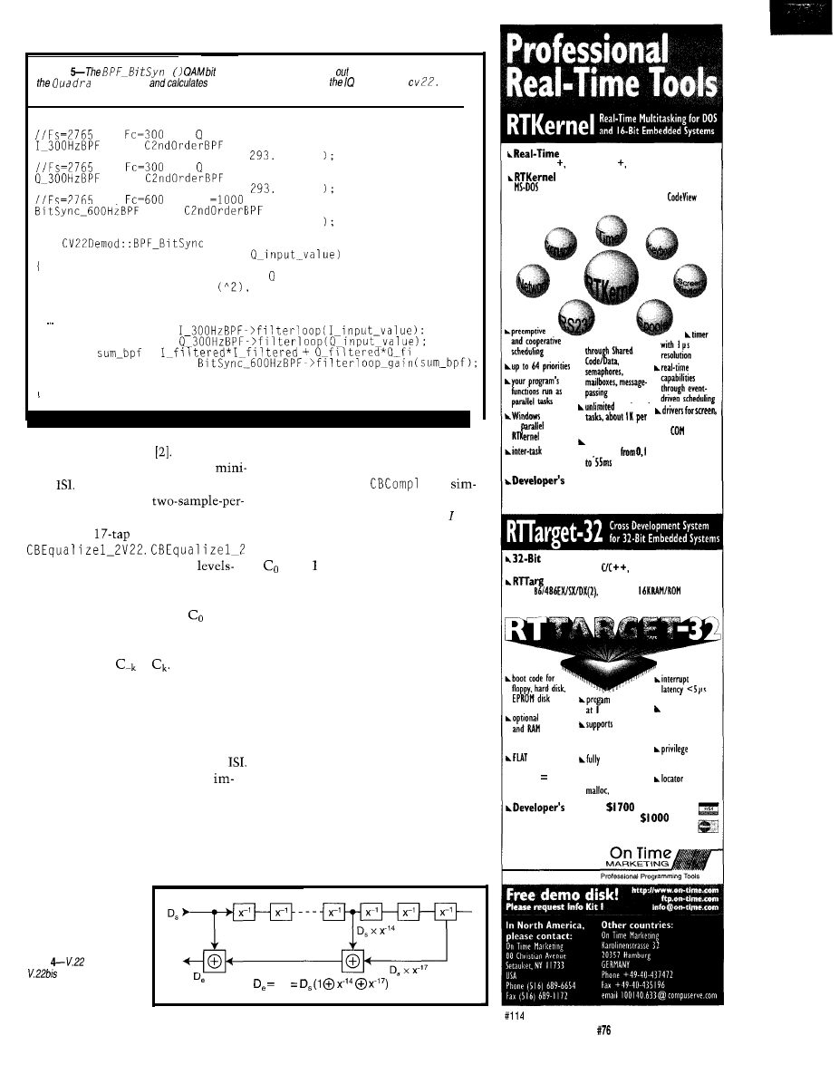
Listing
c
synchronizer decimates three of four output samples from
t u r e Mixer
the optimum time to sample values. See
cpp
for the complete listing.
BPF CONSTRUCTORS:
Hz,
Hz, = 100
= new
(-0.9931839456, 1.5448876939,
Hz,
Hz, = 100
= new
(-0.9931839456, 1.5448876939,
Hz.
Hz. Q
= new
(-0.9864142558, 0.4002915270,
4248888
147. 2131352
4248888
INT
(double I-input-value, double
//routine to band-pass filter I and arms,
then square each output
//add results and band-pass filter at symbol rate = 600 Hz
(calculate filter values every fourth sample)
double I-filtered =
double Q-filtered =
double
=
ltered;
double baud-filtered =
(remainder detects zero crossings and interpolates I and C! values)
creating additional IS1
The equal-
symbol complex linear adaptive-equal-
izer using a
complex FIR filter in
izer tries to adjust its response to
also uses the equalizer for the
mize
to-bits and bit-sync functions.
We implemented a
register in the filter contains the and
est overall mean squared error from
Q values as a complex number.
the expected constellation points.
A complex class,
ex,
plifies the mathematics. Each storage
The equalizer algorithm starts with
set to and all other coefficients to 0.
Once per symbol, the equalizer calcu-
lates the output symbol from the sum of
the coefficients times the tap values.
A nine-symbol equalizer (17 taps]
worked well. The center tap con-
tains mostly energy from the current
symbol and some from the past and
future symbols
to
The equalizer adds the current-sym-
bol center tap with scaledversions of the
past and future symbols. With the cor-
rect symbol clock and tap coefficients,
the energy from past and future symbols
can be subtracted out, reducing the
Figure 5 shows how an equalizer
proves the SNR of a V.22 signal.
The output symbol is subtracted
from the closest point in the constella-
tion (DDF). This produces a complex
phase-error vector that is scaled by a
small value (0.2).
The scaled error is multiplied by each
tapped value in the filter and added to
the coefficients. The complex phase
error is also used as the feedback signal
for the NC 0 carrier-tracking loop.
Our complex linear adaptive equal-
FRAME SYNC
izer (see Figure 6) uses the minimum
mean squared error to calculate the
new tap coefficients. The equalizer
converges to the
coefficients pro-
ducing the small
The frame synchronizer recognizes
a valid frame marker and groups the
demodulated bits into data blocks.
Figure
and
modems use a
shift register to descramble
the transmitted bit.
D ,
Multitasking for:
Borland C/C+ Microsoft C/C+ or Borland Pascal
supports:
3.0 or higher, Embedded Systems without DOS,
Paradigm Tools (info available), Turbo Debugger,
can run
n u m b e r o f
i n
with
task needed
keyboard, up to
tasks
38
ports, IPX
timer rate
services, floppy
a d & a b l e
disks, hard disks,
communication
etc.
License:
5550
complete Source Code: add $500
no run-time royalties
Development System for:
B o r l a n d U C + + , M i c r o s o f t
W a t c o m U C + +
et-32 supports:
Intel 38
as little as
d o w n l o a d
1 5 2 0 0 b a u d
serial
paging
standard
communications
remapping
PCs and controller
library
boards
memory
level
model with
supports the
0 or 3
C/C+ + run-time
physical logical
systems (printf,
for Win32
addresses
etc.)
PE-files
License:
complete Source Code: add
no run-time royalties
C i r c u i t C e l l a r I N K @
Issue
November 1996
27
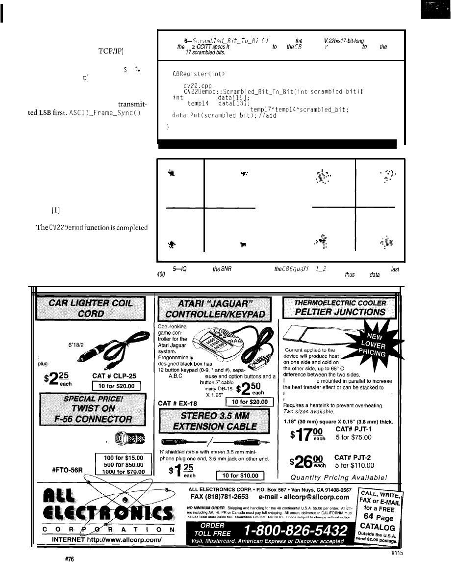
Data blocks and frame markers are
defined as part of the communications
protocol (e.g., ASCII or
and are
not part of the modem’s specifications.
The CASCII class (found
in
c a c i
h
and
c
a
s c i i . c p
contains the ASCII
frame-sync code to detect the start of the
ASCII character or data block and re-
verses the bits since ASCII is
returns an integer equal to the ASCII
character value of the data block.
For ASCII asynchronous data, the
mark condition or no transmitted data
is al, the same as a stop bit. The pat-
tern 10 occurs if two data blocks are
sent immediately after one another or
if there is a period of no transmitted
data followed by a valid data block.
ASCI I_Frame_Sync
searches for a
stop bit and start bit (0) followed by
eight data bits.
after the ASCII value is returned. The
program has several options to display
the demodulated bits or ASCII data to
Listing
t implements V.22 and
descrambler
previous
from V.22
ecs. demonstrates how use Reg is t e template class store
From cv22.h header file
data:
//defines data as integer register
From
int
temp17 =
int
=
//seventeenth storage location
//fourteenth storage location
int unscrambled-bit =
scrambled bit to register
return unscrambled-bit;
the screen or a file for testing and anal-
ysis like a simple data analyzer.
Figure
plots show
improvement using
ze
adaptive-equalizer class. The
symbols are plotted. Adaptive equalizers allow for denser symbol constellations and
higher
rates.
Heavy-duty cigarette lighter plug with remov-
able
AGC
2 amp fuse.
Will handle
higher current with larger
fuse. Black,
SPT-2 cord with
2.5 mm co-ax
rate
buttons, p
four-way direction
terminated with hi-de
connector. 6.5” X 5”
Modules can b
achieve high differential temperatures. 127 ther-
mocouples per device. Operates on 3-12 Vdc.
We recently made a large
purchase of this twist-on co-ax
connector for RG-6 cable.
Special pricing while
the supply lasts.
CAT
CAT# CB-357
1.57” (40
mm) square X
0.15” (3.8 mm) thick.
28
Issue
November 1996
Circuit Cellar INK@
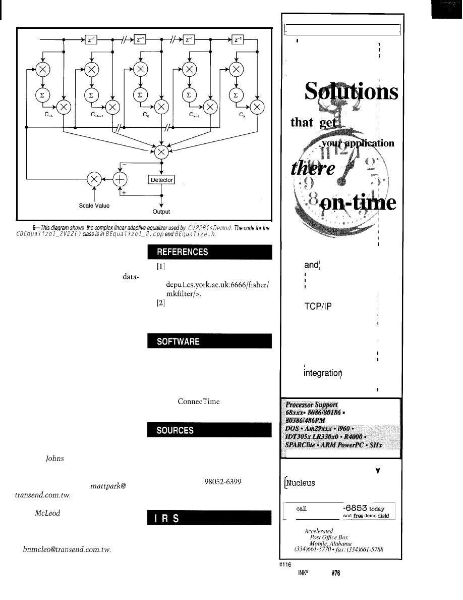
Input
Figure
Watching the ASCII characters gives
feedback about the demodulated bits.
For embedded systems, add a custom
frame marker, data-block detector,
logging capability, or other data-process-
ing functions to the demodulated bits.
WHERE TO GO FROM HERE
We aren’t done optimizing the real-
time code. A few routines could ben-
efit from some assembly language.
We’ll next experiment with higher
speed QAM modems since C
V 2
2 Demod
is almost already a generic QAM de-
modulator. The idea of real-time fax
demodulation is intriguing.
We hope you’ve gained some ideas
on how you might use DSP in your
own embedded controllers and com-
munications projects.
q
Matt Park holds a BSEE from The
Ohio State University and an MSEE
from The
Hopkins University.
He is an engineering consultant for
communications and electro-optics.
You may reach Matt at
Brian
holds a BSEE from Ak-
ron University and is an engineering
consultant for communications and
signal processing. You may reach him
at
G. Fisher, “Interactive Filter
Design Web Page,” <http://
J.G. Proakis, Digital Communi-
cations,
McGraw-Hill, New
York, NY, 1983.
Software from this article can be
downloaded from the Circuit
Cellar BBS, the Circuit Cellar
Web site, and from Software on
Disk for this issue. Please see the
end of
for down-
loading and ordering information.
Visual C++ 4.0, Visual C++
1.52,
Windows 95, Windows NT
Microsoft Corp.
One Microsoft Way
Redmond, WA
(206) 882-8080
Fax: (503) 244-726 1
404
Very Useful
405 Moderately Useful
406 Not Useful
Accelerated Technology, Inc.
Real-Tim&
I
I
Nucleus RTX
Real-Time Kernels
Nucleus NET
Real-Time
I
I
I
I
Real-Time Software]
800-468-6853
d
for more information and
demo
Technology, Inc.
850245
36685
Circuit Cellar
Issue
November 1996
2 9
Frank Gao
Algorithms and Software
for V.34 Modems
merest in soft-
ware implementa-
flexibility and attractive cost-perfor-
mance ratios software modems offer.
Traditionally, implementations of
modem and fax data pumps are burned
into dedicated chip sets. Engineers
using these off-the-shelf,
mable chips can usually ignore their
internal operational mechanisms.
But, with the increasing popularity
of the software implementations of
modem and fax, designers need to
understand their operational principles
and software building blocks.
In this article, I present the major
signal-processing functions a V.34 data
pump requires and its software imple-
mentation. The principles are common
to other fax/modem techniques, but I
use V.34 software from GAO Research
and Consulting as an example.
V.34 MODEM HANDSHAKING
The V.34 modem data-pump soft-
ware is composed of three parts-the
handshaking, the transmitter, and the
receiver.
The V.34 modem startup has four
phases. Phase
1
is defined in ITU V.8, a
universal
scheme for mo-
dems, faxes, and other communica-
tions devices. Phase 2 sets the modem
parameters and performs line probing
and ranging. Phase 3 is used for initial
training of the equalizer and echo
canceler, and Phase 4 offers the final
training and exchange of data-mode
modulation parameters.
V.34 MODEM TRANSMITTER
The transmitter’s structure (see
Figure
1)
follows the ITU V.34 stan-
dard. It has five parts-the scrambler,
framer, encoder, filter, and modulator.
The scrambler randomizes the in-
put binary data to spread the
signal spectrum over the transmit
band. It facilitates effective transmis-
sion of data over the telephone chan-
nel and improves the convergence of
the adaptive equalization and echo
cancellation in the receiver.
The framer includes a superframe, a
data frame, and a mapping frame. The
superframe consists of seven or eight
data frames for different symbol rates.
The data frame has
12-16
mapping
frames for different symbol rates. The
mapping frame has four 4D symbol
intervals, each consisting of two 2D
symbol intervals.
The encoder consists of a shell
mapper, a differential encoder, a
coder, a Trellis encoder, and a nonlin-
ear encoder. Three new techniques are
employed in the encoder-multidi-
mensional Trellis-coded modulation
(MD-TCM), shell mapper, and
ing equalization.
MD-TCM combines coding and
modulation so the modem benefits
from high reliability with limited
transmission frequency bandwidth.
The standard recommends three con-
volutional encoder structures for the
transmitter. The three Trellis
32-state
and
all with 4D QAM
constellation-can achieve asymptotic
coding gains of -5
Scrambler
Framer
Encoder
Filter
Modulator
Figure l--The transmitter of the V.34 modem processes the data to be transmitted minimize the effects of
channel noises and improve the convergence of the adaptive equalization and echo cancellation in the receiver.
30
Issue
November 1996
Circuit Cellar INK@
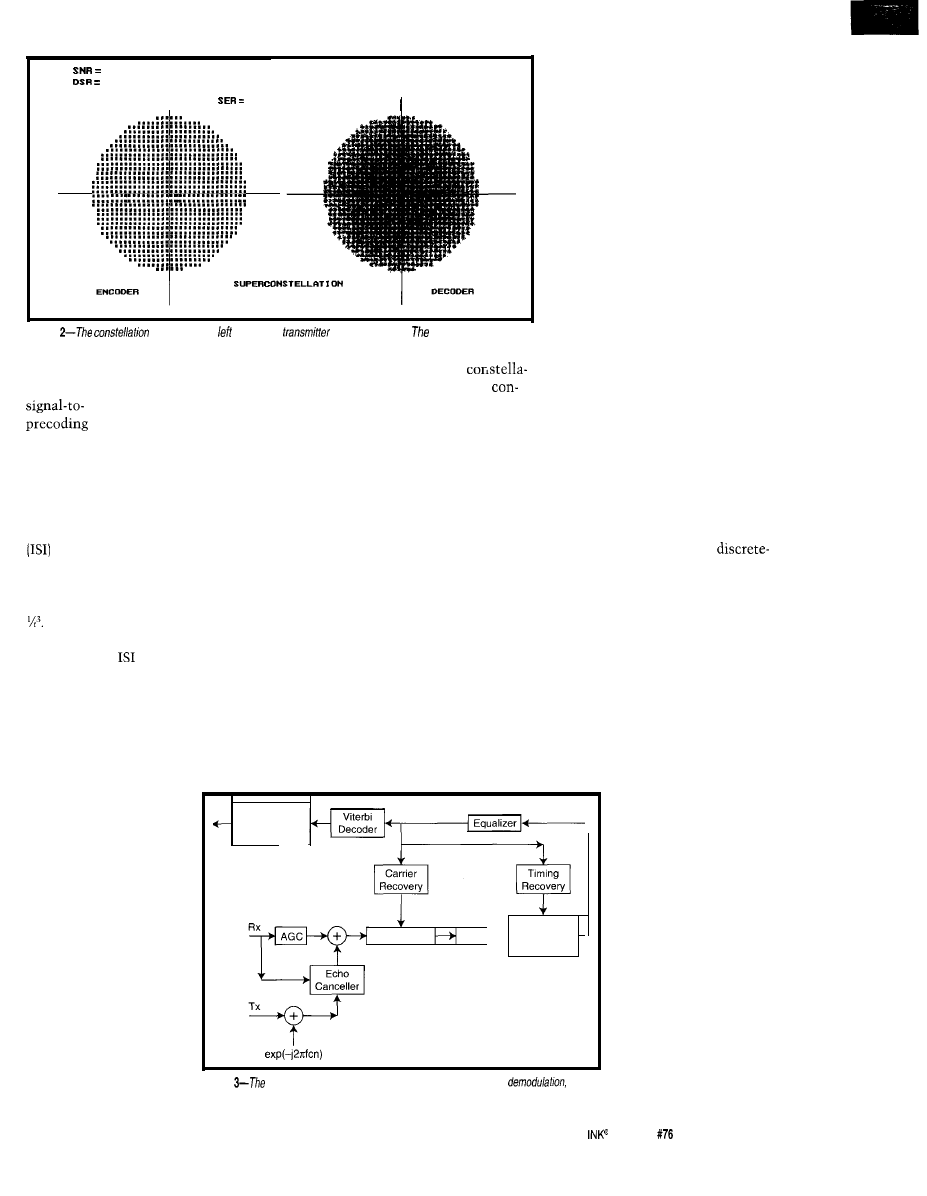
3 0
945
2 8 8 0 0
0 . 0 1 5 7 0 7 5 8 4 0 9 7 9 8 1
I
0 . 0 0 0 0 4 1 3 3 5 9 7 7 5 8 5
Figure
diagram on fhe is from the
of a V.34 modem.
one on the right is
from the receiver.
Shell mapping reduces the average
Figure 2 shows the signal
signal energy and improves modem
tion for the V.34 modem. Signal
performance with the same
stellations consist of complex, valued
noise ratio. The
technique, a
s i g n a l p o i n t s .
nonlinear equalization scheme, re-
duces the effects of noise enhancement
i n t h e e q u a l i z e r .
The pulse-shaping low-pass filter in
Figure 1, called a raised cosine filter,
eliminates intersymbol interference
on the band-limited PSTN.
The point with the smallest magni-
tude is labeled 0, the point with the
next larger magnitude is 1, and so on.
When two or more points have the
same magnitude, the point with the
greatest imaginary component is first.
Unlike the ideal pulse-shaping fil-
ter, the raised cosine filter is realizable
and has tails of decay proportional to
So, the timing errors in the modem
have a much less dramatic effect on
the amount of
in the raised cosine
filter. The pulse-shaping filter usually
spans four baud intervals.
V.34 MODEM RECEIVER
The ITU V.34 modem uses quadra-
ture amplitude modulation (QAM) in
the transmitter and receiver. The en-
coded digital sequence is amplitude
modulated and con-
verted to analog signal
for transmission.
The ITU V.34 standard doesn’t
specify the receiver’s structure, so the
implementation is more flexible.
As shown in Figure 3, the receiver
is a more complicated component.
Several functions are the inverse of the
transmit functions. The receiver con-
sists of seven major functional blocks.
The AGC operates over a wide
dynamic range and maintains the out-
put signal at a constant level necessary
The samples received by the mo-
dem suffer from IS1 which results from
the linear amplitude and phase disper-
sion in the channel. These broaden the
transmitted signals and cause them to
interfere with one another.
To increase transmission perfor-
mance, a filter estimates the channel’s
inverse transfer function and performs
channel equalization. Usually, a linear
adaptive transversal filter is used. Its
coefficients are adjusted by the Least
Mean Square (LMS) algorithm.
The purpose of timing recovery is to
recover a clock at the symbol rate or a
multiple of the symbol rate from the
modulated waveform (see Figure 4).
This clock converts the received con-
tinuous-time signal into a
time sequence of data symbols.
Timing recovery imposes require-
ments on the modulation technique
not present when a separate clock is
available. The strength of the timing
information in a signal is affected by
the statistics of the signal, line code,
and pulse shape.
The double-sideband
QAM in the V.34 mo-
dem is an efficient mod-
ulation technique in
terms of bandwidth. In
QAM, two quadrature
carriers are modulated
by two separate informa-
tion-bearing signals-the
real and imaginary parts
of QAM. The V.34 mo-
dem signal set was de-
signed to give enough
distance between mem-
bers of each subset.
Inverse Framer
and
Descrambler
In pass-band systems, the carrier
frequency is generated by a timing
reference in a transmitter. Coherent
demodulation of a pass-band signal
requires the same carrier
frequency and phase to
perform the demodulation.
If symbol timing is
known, carrier frequency
can be derived. Symbol
timing can be derived with-
out knowing the carrier
phase. When a receiver
starts receiving data, it
should derive the timing
before estimating the carrier
phase and adapting the
equalizer.
Interpolating
Demodulator
AGC
Decimating
Filter
Figure
receiver of a V.34
modem performs such functions as
decoding, echo cancellation, equalization, and carrier and timing recovery.
for the proper operation of the receiver
algorithms. In the receiver, several
modules use amplitude thresholds to
make their decisions.
Receive signals are typically ad-
justed by two AGC stages. The first
signal is set during training and re-
training, and the second is dynami-
cally adjusted.
The hybrids in a typical
telephone system cause
near- and far-end echoes,
which are harmful for data
Circuit Cellar
Issue
November 1996
3 1
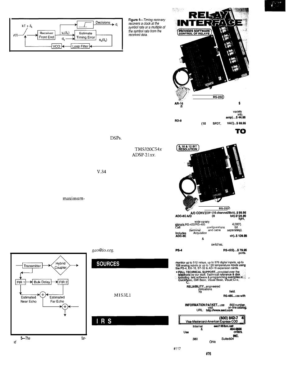
transmissions over telephone net-
works.
The far-end echo canceler is weaker
than the near-end echo. However, the
far echo may be frequency translated
when it passes through frequency
converters (i.e., modulators and de-
modulators) on the four-wire circuits.
This phenomenon, called phase roll
or frequency offset of the far echo, is a
nonlinear impairment. So, nonlinear
compensation techniques must be
used for far-echo cancellation.
Near- and far-end cancelers elimi-
nate the echoes. The echo cancelers
use the received and delayed transmit-
ted signals to estimate the echoes.
They cancel them by subtracting the
estimated echo signals from the re-
ceived signals as shown in Figure 5.
To model the echo response pre-
cisely, the echo canceler must be
trained using adaptive algorithms. The
LMS algorithm is most widely used
because of its computational efficiency.
The Viterbi decoder is a
likelihood decoder used in the V.34
modem. It chooses the symbol se-
quence most like the transmitted sig-
nal sequence via some metric (e.g., the
minimum Euclidean distance).
The symbol sequences in the V.34
modem consist of 4D symbols. One
4D symbol is the concatenation of two
Remote Signal
+ Echoes + Noise
Remote Signal + Noise
gure
echo canceler consists of
Rear-
and
cancelers.
consecutive 2D symbols which are
points in the QAM constellation.
V.34 MODEM IMPLEMENTATION
The increased interest in the V.34
modem technology has been partially
due to such new applications as the
DSVD modem and H.324 video phone.
GAO has developed V.34, DSVD, and
H.324 software for DSP- or micropro-
cessor-based soft modems.
The software has three versions.
One version, coded in ANSI C, is for
Pentiums, microprocessors, and float-
ing-point
The two others are
coded in the DSP assembly languages
of Texas Instruments’
and Analog Devices’
SOFTWARE-MODEM MARKET
modems have been driving the
modem market since ITU released the
standard in 1994. This should continue
another six or seven years.
Software implementations of V.34
offer attractive cost-performance ratios
and flexibility. I believe they’ll soon
play a more significant role than mo-
dems with fixed-function IC chips.
q
Frank Gao is the founder and CEO of
GAO Research and Consulting, a
leading supplier of software-modem
technologies. You may reach Frank at
V.34
modem and software
GAO Research and Consulting, Ltd.
55 Nugget Ave., Ste. 204
Scarborough, ON
Canada
(416) 292-0038
Fax: (416) 292-2364
407
Very Useful
408 Moderately Useful
409 Not Useful
(CO
NNE
C
T
S
To
RELAY INTERFACE (16 channel) . . . . . . . . . . . . 89.96
Two channel (TTL level) outputs are provided for
connection to relay cards or other devices (expandable
to 128 relays using EX-16 expansion cards). A
of
relays cards and relays are stocked. Call for more
AR-2 RELAY INTERFACE (2 relays, 10
REED RELAY CARD (6 relays, 10 VA) . . . . . . $49.96
RH-8 RELAY CARD
amp
277
A N A L O G
D I G I T A L
,
( C O N
N E C
TS To
A D G 1 6
CONVERTER* channel/IO
Input voltage. amperage. pressure, energyusage.
joysticks and a
of other types of analog
available (lengths to
for info on other AID
and 12
converters
block
sold
Data
software for Windows 95 or 3.1
TEMPERATURE INTERFACE* (8
Includes term. block 8 temp. sensors (-40’ to 146’ F).
STA-8 DIGITAL INTERFACE’ (8 channel) . . . . . . . . . $99.96
Input on/off status of relays,
HVAC equipment,
security devices, keypads, and other devices.
PORT SELECTOR (4 channels
Converts an RS-232 port into 4 selectable RS-422
CO-422 (RS-232 to RS-422 converter) . . . . . . . . . . . . . . . . . . . $ 39.96
l
EXPANDASLE...expand your interface to control and
Turbo
Assembly and others are provided.
l
HIGH
for continuous 24
hour industrial a
with 10 years of proven
performance in t energy management
. CONNECTS TO US-232 RS-422 or
IBM and compatibles, Mac and most computers. All
standard baud rates and protocols (50 to 19,200 baud).
FREE
our
Fax or E-mail to order, or
our Internet
Technical Support (614) 464-4470
24 HOUR ORDER LINE
842-771
E-mail:
international Domestic FAX: (614)
for information, technical support 8
ELECTRONIC ENERGY CONTROL,
South Fifth Street,
Columbus,
43215-5491
Circuit Cellar INK@
Issue
November 1996
33
Empowered
Digital
Filtering
Brian Senese
0
ilter design using
DSP techniques is
very simple if you can
calculate the coefficients
necessary for its implementation. I
find it frustrating, however, after read-
ing about digital filters, to discover
that the most critical information (i.e.,
the filter coefficients) isn’t readily
available.
In this article, I’ll discuss filter
design and provide you with a
based software tool that calculates
coefficients. The many facets of digital
filtering should be treated as simply as
they’re presented. General filter deri-
vation, sampling theory, and coeffi-
cient quantization are topics best left
for your own investigation.
BASIC SAMPLING
To begin, let’s explore a basic sam-
pling system. A typical configuration
consists of front-end preparation, sig-
nal processing, and back-end signal
reconstruction.
Preprocessing the analog signal
involves passing signal energy through
an antialias filter, which removes
frequency components above the high-
est frequency the digital filter can
handle.
Next, a sample-and-hold function
makes a copy of the signal at a particu-
lar instant in time and holds this
Figure
waveform
is sampled at a
sampling rate, capturing
relevant frequency information.
ple, so it provides a steady signal to the
ADC.
The ADC then transforms the ana-
log signal into its digital counterpart,
so it’s ready for processing. The rate at
which analog signals are sampled is
often governed by a timer, ensuring
that samples are taken at constant and
periodic intervals.
The processor manipulates this
signal, as in the case of filtering, and
writes the result to a DAC, which
generates an associated analog value.
Because digital values are written at
periodic intervals, the analog output of
the DAC appears stepped.
A reconstruction filter smooths the
step-like response. That is, all
frequency components created as a
result of the D/A transformation are
removed.
The maximum frequency acceptable
for processing by the filter is linked to
the sampling rate and defined as:
Max frequency= Sampling rate
2
Removing analog-signal energy
above the maximum frequency pre-
vents aliasing from corrupting the
desired filtered result. Sampled sys-
tems are characterized by this effect.
Signal energy appearing above the
maximum frequency is reflected back
into the frequency band of interest.
The analog signal is captured through
a sample-and-hold process that freezes
the analog-signal level, allowing an
accurate conversion by the ADC from
its analog to digital representation.
The digital word’s size determines
many things-most importantly, the
signal-to-noise ratio (SNR) of the sys-
tem. For example, 16-bit representa-
tions take longer to convert from the
analog source and are often more ex-
pensive to implement.
However, they yield superior re-
sults. As a general rule, 6 of SNR is
Waveform Frequency 10
Sample Rate 20
m s
0.1 ms
0.15
0.2 ms
0.25 ms
X ( 2 ) =
X ( 4 ) =
34
Issue
November
Circuit
Cellar
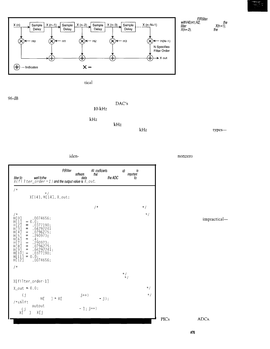
Addition of Digitized Signals
0
Indicates Multiplication of Digitized Signals
gained for every bit in the sample.
That is, 16 bits of unsigned data de-
fines a system capable of achieving a
SNR.
The processor reads and stores this
sample, using it to calculate the next
filtered value to be written to the DAC
for signal reconstruction. Several input
samples taken at consecutive time
intervals are required to generate a
single output value.
Reconstruction of an analog sig-
nal-the final step-is accomplished
by writing the calculated digital-value
to that used in capturing the
original analog waveform. A low-pass
filter inserted at the output of the
DAC removes unwanted harmonics
generated by the
step action.
A
sinusoidal waveform
requires the sample rate to be at least
20
(see Figure
1).
All signal energy
from 0 Hz to 10
is also captured.
Signals appearing above
10
alias back into the band of interest and
cause distortion. But, an antialiasing
filter prevents this.
So, in a basic sampling system, you
stream to a DAC at a sample rate
should remember to:
Listing l--This
routine is a realization of a
of
order 13.
are set prior execution
and are extracted from the filter-design
Note coefficient accuracy is very
for your
respond
original specification. The
value read from
is assigned
placeholders for sampled data, filter coefficients, and
final value
double
int filter-order;
t coefficients for the filter as provided by the software
=
filter-order = 13;
define filter order
se
=
Run this code segment after reading ADC value. Each value (and
preceding value) is used to calculate the filter output. All
data values are shifted before next calculation.
/*data input value is digitized sample read from ADC
= data input value;
/*clear calculated value
I
for = 0; j < filter-order;
/*calculate filter output
X out += j filter-order 1
all data sample values in the filter before generating next
filter
value*/
for = 0: ‘j < filter-order
j =
+ 11;
Figure 2-A
is represented
and so on being
coefficients and X(n),
and so on being ADC data
samples.
l
sample at a rate slightly
greater than twice the max-
imum frequency you wish
to process (this gives you a
safety margin since digital
filtering is an imperfect process)
l
filter the incoming analog signal and
eliminate any energy above the
maximum frequency as defined
earlier
l
filter the output of the DAC to re-
move generated harmonics
FILTER CONCEPTS
There are two basic filter
Finite Impulse Response (FIR) and
Infinite Impulse Response (IIR).
FIR filters are labeled as finite be-
cause an output is generated only as
long as a
sample is present in
the filter. They are the easiest filters to
design and are generally used in com-
munications-specific applications. In a
modem design, for example, the filter
output displays a desirable linear phase
response over frequency.
FIR filters require more coefficients
than IIR filters to realize the same
filter-response characteristic. More
processing cycles and memory are
needed, making the implementation of
FIR filters sometimes
especially for microcontrollers.
IIR filters use feedback to generate
an output. They have an infinite re-
sponse since energy is always fed back
into the filter. They require fewer taps
(or stored signal samples)
to
realize the
same response as an FIR filter.
One disadvantage of an IIR filter is
in its group-delay characteristic. The
output-signal phase response is nonlin-
ear over the frequency band, and this
characteristic is undesirable for com-
munication systems.
IIR filters are an excellent choice for
data-acquisition systems and are best
suited for embedded-microcontroller
systems. The PIC application hand-
book outlines an IIR design for use on
equipped with
Circuit Cellar INK@
Issue
November 1996
35
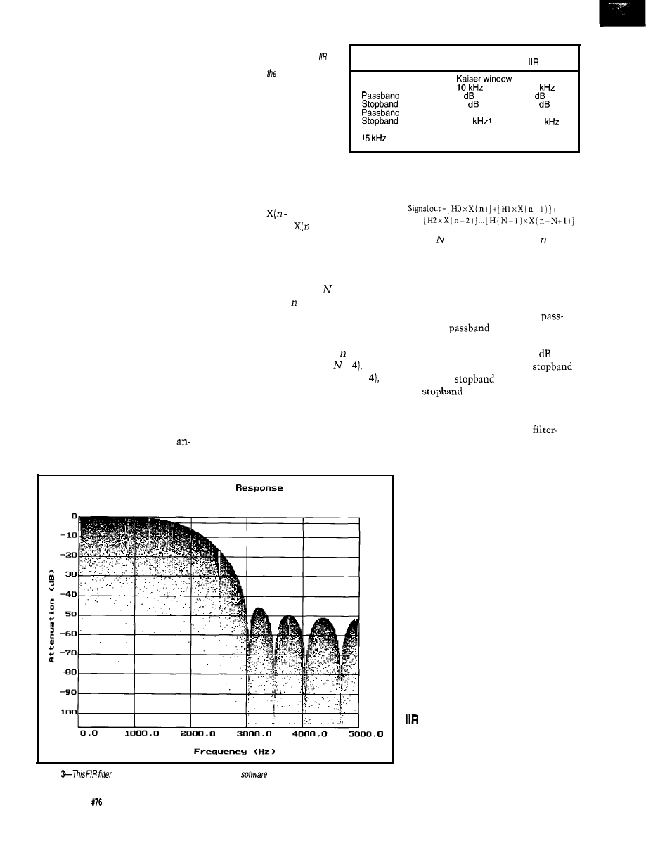
Filters are defined mathematically
and use a series of past data-sample
values with a set of filter coefficients.
Through a series of multiplications
and additions, a singular, filtered out-
put value is generated each time a new
input is read. All processing must be
completed before the next data sample
is made available from the ADC.
The algorithm is interrupt driven,
with the interrupt source being a clock
that determines the sample rate. On
invoking the routine, the previously
calculated data point is written to the
output DAC.
A new data sample is read from the
ADC, calculations are made, and a
new output value is generated. This
value is held in memory until the next
interrupt cycle.
The routine then shifts all sampled
data in preparation for the new data
value to be read in on the next cycle.
Following that, the routine waits for
the next interrupt.
Variations on this theme are pos-
sible. Other processes or instructions
can be executed in place of the wait
state I use. The most important rule of
the system is that the filter interrupt
routine must be serviced immediately
and allowed to complete before
other filter interrupt is generated.
Table l--These parameters define
fhe desired filter responses for
and FIR filters. Calculated filter
coefficients in examples are
based on
these specifications.
FIR
Low-Pass Filter
System Sample Rate
Butterworth
10
Ripple
1
2
Attenuation
40
30
O-l 000 Hz
O-1000 Hz
3-5
4-5
is half the sample rate.
FIR filters use previous
knowledge of the sampled
signal to generate a fil-
tered version of the incoming signal.
The FIR filter is depicted in Figure 2.
Mathematically, the filter is ex-
pressed as:
X(n) is the digitized value read from
the ADC.
1)
is the previously
sampled value,
2) is the value
read two sample periods ago, and so
on. The filter order (or length) deter-
mines the roll-off response. Larger
filter orders provide better filter char-
acteristics. In Figure 2, defines the
filter order and identifies the sample
just taken.
Imagine, for example, that the ADC
presents the sample marked as X(5)
from Figure
1.
In this case, is 5 and,
for a filter order of 4 (i.e., = you
require previous sample values X(
X(3), and X(2). These values are used to
compute the next single output value.
The next sample read by the proces-
sor would be X(6). All sample values
inside the filter must shift to the right
for the new calculation to be correct.
F i l t e r
Figure
response is generated by fhe filter-design
using fhe simulation mode of operation.
36
Issue
November 1996
Circuit Cellar INK@
where is the filter order and repre-
sents the current sample value.
An FIR filter design starts by defin-
ing parameters that govern its perfor-
mance.
For instance, you must know how
much ripple is tolerable in the
band, the
frequency (the
frequency where the filter attenuates
the signal by approximately 3 with
respect to the passband), the
frequency,
attenuation, and
the
ripple. The system sam-
ple rate must also be known.
After specifying all filter param-
eters, enter the values into a
design program. It first determines the
filter order required to provide the
desired response.
Then, it generates the coefficients
for the filter. The order of the filter
tells you how many taps to include in
the algorithm. The filter coefficients
are entered as constants.
The code segment in Listing
1
(writ-
ten in C) realizes a FIR filter of order
13.
Filter constraints for the design are
shown in Table 1.
Entering these parameters into the
digital-filter program yields a set of
coefficients. These constants are as-
signed to an array which facilitates
easy data manipulation.
Figure 3 illustrates the filter re-
sponse of the designed FIR filter as
presented by the digital filter-design
program.
FILTERS
Designing an IIR filter is very differ-
ent from the FIR design process. An
IIR filter is realized by cascading sec-
ond-order IIR filter sections.
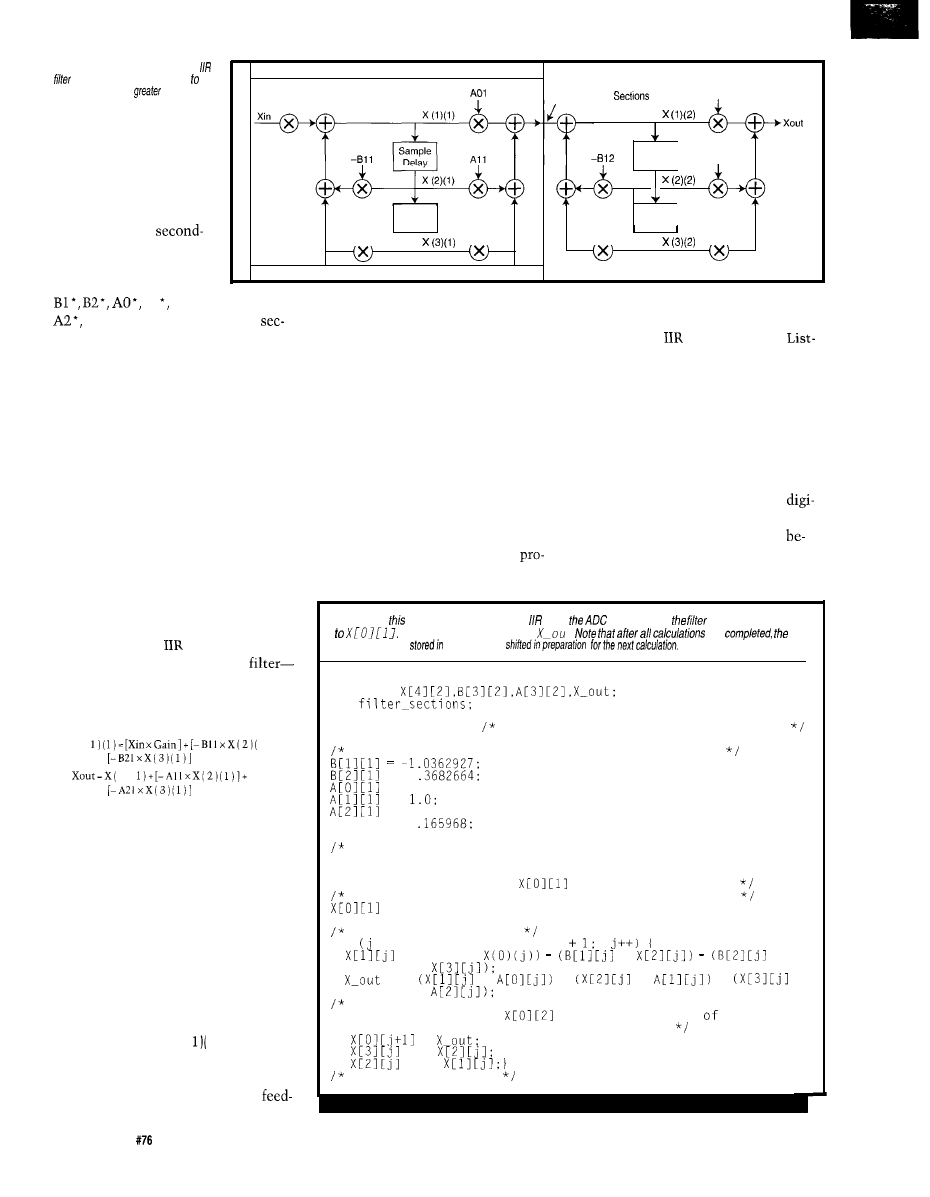
Figure 4-Several second-order
sections can be
cascaded
create
filters of
order which
generate better filter-response
characteristics.
Gain
Second-Order Filter Section
Distribute Gain
Between Filter
A02
Sample
Delay
Al2
-621
Sample
Delay
A21
-822
Sample
Delay
A22
In Figure 4, a
order filter section is
identified. Filter coeffi-
cient values, defined as
Al
and
are associated with specific
back is used by the filter, the input
The code segment realizing the
ond-order filter sections.
signal Xin must be reduced to prevent
second-order
filter is given in
In Figure 4, the second identifying
filter instability. It is recommended
ing 2. Filter constraints for the design
integer is linked to the filter-order
that in an actual filter design of order
are shown in Table 1.
section. This link becomes important
greater than 2, the Gain be spread
The filter-response plot generated
when assigning coefficients to the
across several sections equally.
by the filter-design software displays a
filter structure because they’re labeled
If, for example, you’ve generated all
characteristic that adheres very closely
as
such in the filter-design software.
An IIR filter of a given order is sim-
pler than a FIR filter of the same
order, thanks to the use of feedback.
Feedback applied to the incoming
signal has the effect of reducing filter
order.
In other words, it may only take a
fourth-order IIR filter to yield the same
filter response (in amplitude) as an
eighth-order FIR filter.
Designing the
filter is almost
identical to developing the FIR
only the algorithm changes. Math-
ematically, the second-order IIR filter
section can be expressed as
:
X (
1 ) ] +
1)(
Realizing an IIR filter with an order
greater than 2 is accomplished by cas-
cading sections together as illustrated
in the fourth-order filter of Figure 4.
The output of the first second-order
section becomes the input to the next
filter section.
Filters of even greater order are
created by the continued addition of
second-order sections. Note that Xin
(the data sample value from the ADC)
is not the same as the value entering
the first data buffer (X( 1)).
A new coefficient, Gain, now ap-
pears in the equation and is required to
scale the filter response. Because
the filter coefficients and have a Gain
to the specification.
factor of 0.04, use a Gain of 0.2 for the
first section and a Gain of 0.2 for the
ROLL YOUR OWN
second section (providing an overall
You now know how to design
Gain of 0.04). Gain is only shown in
tal filters without experiencing the
one location in Figure 4 to prevent
pain of understanding the theory
confusion since the filter-design
hind their operation. The benefits of
gram provides a single value.
this technology include being able to:
Listing 2-h
example of a second-order filter,
value fed info
algorithm is assigned
The calculated output value is
t.
are
data values
fhe filter are
/*placeholders for sampled data, filter coefficients and final value*/
d o u b l e
int
filter-sections = 1;
specify one second-order filter section
set coefficients for filter as orovided bv software
=
=
0 . 5 ;
=
=
0 . 5 :
Gain =
Run code segment after reading ADC value. Each value is used
(as are preceding data values) to calculate filter output. Data
values are shifted before next calculation. The input value Xin
in Figure 5 is labeled
in following equation.
data input value is digitized sample as read from ADC
= data input value;
Calculate filter output
for = 1;
j < filter-sections
= (Gain *
*
*
=
*
+
*
+
*
Shift data sample values in filter before generating next
filter-output value.
now contains output filter
and can feed the next filter section or DAC.
=
=
=
end of FOR statement
38
Issue
November 1996
Circuit Cellar INK@
l
remove noise from an incoming
signal without expensive hardware
l
adjust the filter response characteris-
tics in real time by simply changing
filter coefficients on-the-fly
l
filter a frequency to eliminate an
unwanted signal [e.g., 60-Hz noise)
Enhancing your data-acquisition
system or embedded-controller appli-
cation through the use of digital filter-
ing is now within your grasp. Consider
yourself empowered.
q
Brian Senese has developed wireless
data-communication systems at
Northern Research and PCSI for the
last eight years. DSP is one of many
technologies that hold his interest. He
may be reached at
Anatoniou, A., Digital Filters:
Analysis and Design,
Hill, New York, N.Y., 1976.
Oppenheim, A.V., and R.W.
Schafer, Digital Signal Process-
ing, Prentice-Hall, Englewood
Cliffs, N.J., 1975.
Williams, C.S., Designing Digital
Filters, Prentice-Hall, Englewood
Cliffs, N.J., 1986.
Software for this article is avail-
able through the Circuit Cellar
BBS, the Circuit Cellar Web site,
and on Software on Disk for this
issue. Please see the end of
for downloading and
ordering information.
Practical Digital Filter Design
Manual
DSP Solutions
13269 Sparren Ave.
San Diego, CA 92129
410
Very Useful
411 Moderately Useful
412 Not Useful
NEWSSTAND PRICE
Upcoming INK issues will feature:
December
Graphics Video
January 1997
Embedded Applications
February 1997
Distributed Control
March 1997
Home and
Building Automation
April 1997
Robotics
our always-popular
BONUS SECTION
covering the Embedded PC market
One year (12 issues) for only $21.95
$31.95 Canada Mexico, $49.95
other non-U.S. addresses
(U.S. funds drawn on U.S. bank)
IT’S EASY TO SUBSCRIBE!
Tel:
875-2188
l
Fax:
871-0411
l
BBS:
871-l
or visit our web site at:
Circuit Cellar INK@
Issue
November 1996
39
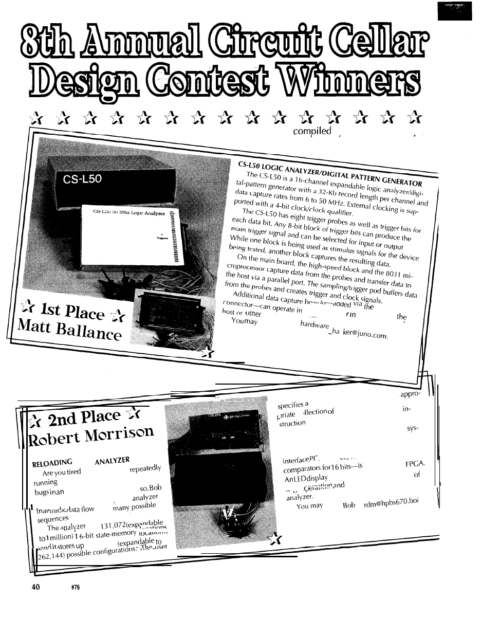
bv Elizabeth Laurencot
expansion boards
dependently
o
expansion
reach
Matt
at
tandem with
c
STATE
of
wasting time
state analyzers to locate firmware
embedded processor! If
designed a small reloading state
__
over
before initiating tracing.
has
to 65,536
tree of possible outcomes
and
states for all expected
co
sequences. That is,
all known possible
trigger sequences are stored and the target
tem is run only once.
The reloading state
analyzer
-including state
interface match configuration,
and
stored in one
provides constant feedback
target
recording status of the
reach
at
hp.com.
issue
November 1996
Circuit Cellar INK@
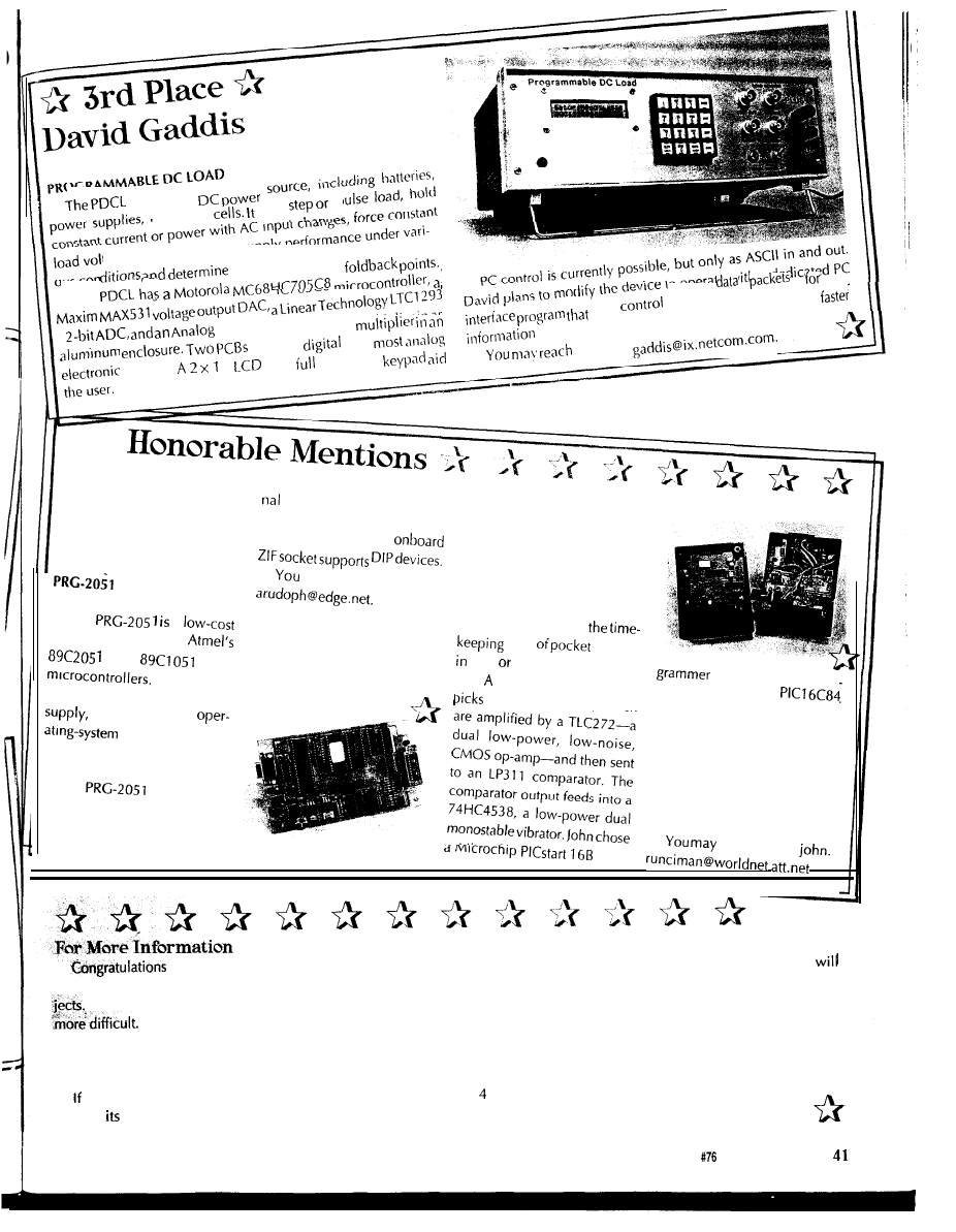
William
Rudolph
DEVICE
PROGRAMMER
program the device. An
may reach William at
Runciman
The
a
device programmer for
and
flash
The single-
board design includes a
power
and the device is
independent. The
user interface shows all device
functions in a single help screen.
The
connects to a
computer via DE-9 female con-
nector. After setting up a term;-
POCKET-WATCH TIMER
This timer measures
error
watches
plus
minus
seconds per
day. clipped-on microphone
up tick vibrations, which
and MPLAB to pro-
gram and debug a
microcontroller for this small,
low-power project.
After a 4-s test period, the
error displays on the top line of
the LCD,
while the frequency
mode is shown
on the bottom
line.
pro-
reach John at
tests any
and solar
can
P
current limits and
codes and
,
hold all
and
Devices AD633 analog
uses
c
o m p o n e n t s
,
6
and
n u m e r i c
exchange.
David at
emulator and uploading an
Intel hex file, you’re ready to
John
to all the winners. From analyzers and testers
wait for the full article to appear in an upcoming issue. We
to programmers, the entries encompassed a wide range of pro-
not give out the phone numbers or addresses of the project
No two
were alike-and that made judging them all the
designers.
If you don’t have E-mail access, we’ll forward your letter to
We encourage all Design Contest winners and entrants to
the designer. Just send it care of:
write complete articles about their projects. Design Contest
Design Contest Winner
articles are highlighted with the finish-line logo.
Circuit Cellar INK
you’d like more information about a project, you may
Park St.
contact designer via E-mail. Otherwise, you must patiently
Vernon, CT 06066
Circuit Cellar
INK”
Issue
November 1996

Kenneth Baker
Self-Tuning PD Algorithm
for the
. very control
engineer is familiar
with the problem of
tuning the parameters of
a
digital controller to suit the charac-
teristics of a specific plant. Parameters
perfect in one system may be wildly
unstable or ineffective in another.
The engineer adjusts the control
parameters by trial and error-guided
by instinct and experience, sometimes
using heuristic rules-until the plant
exhibits the desired behavior. The
controller is then sent to the plant
with the assumption that it will re-
main reasonably constant.
But, what if that assumption turns
out to be false? Many systems have
characteristics that change with power
supply, mechanical load, or wear on
the parts. In these cases, the quality of
the control may degrade because the
controller is no longer properly tuned.
We need a self-tuning controller that
automatically deduces a plant’s charac-
teristics and adjusts control parameters
to maintain the desired behavior.
The self-tuning control algorithm I
present starts with a discrete-time
proportional-derivative (PD) control
algorithm. Piggybacked on that is a
recursive least-squares (RLS) algorithm
borrowed from adaptive DSP theory,
which estimates the plant’s character-
istics from its I/O datastreams.
The PD and RLS algorithms are
well known and understood. What’s
not obvious is how to feed the results
of the RLS back into the PD.
SYSTEM ANALYSIS
Figure 1 shows a typical system.
Signal d(k) is the desired plant output,
and y(k) is the actual output. The error
signal x(k) is the difference between
these outputs. The error signal is usu-
ally represented as e(k), but I’m reserv-
ing that symbol for something else.
The controller output is u(k).
For all signals, I prefer to normalize
full scale to 1. That way, the control
algorithm can run independent of the
application. Other software in the
controller can include scaling factors
as necessary.
In discrete time, the plant output is
described by:
y ( k + l ) = - a y ( k ) + b u ( k )
where
a
and
b
are the plant param-
eters. The controller function is de-
scribed by:
where and are the respective
proportional and derivative control
parameters.
Assuming the controller can main-
tain this plant at all, the output y(k)
eventually reaches a steady state in
response to a step input in d(k), at
which time x(k) = 0 within some band
of tolerance. But, “eventually” doesn’t
necessarily constitute good, predict-
able control.
I’d like to optimize the plant’s tran-
sient response to a step input accord-
ing to a defined measure by specifying
the desired response time and over-
shoot.
In general, analytical solutions to
discrete-time equations aren’t possible,
so to describe the transient response,
Figure
a
feedback
system, the
target and
plant outputs are d(k) and y(k),
respectively.
4 2
Issue
November 1996
Circuit Cellar
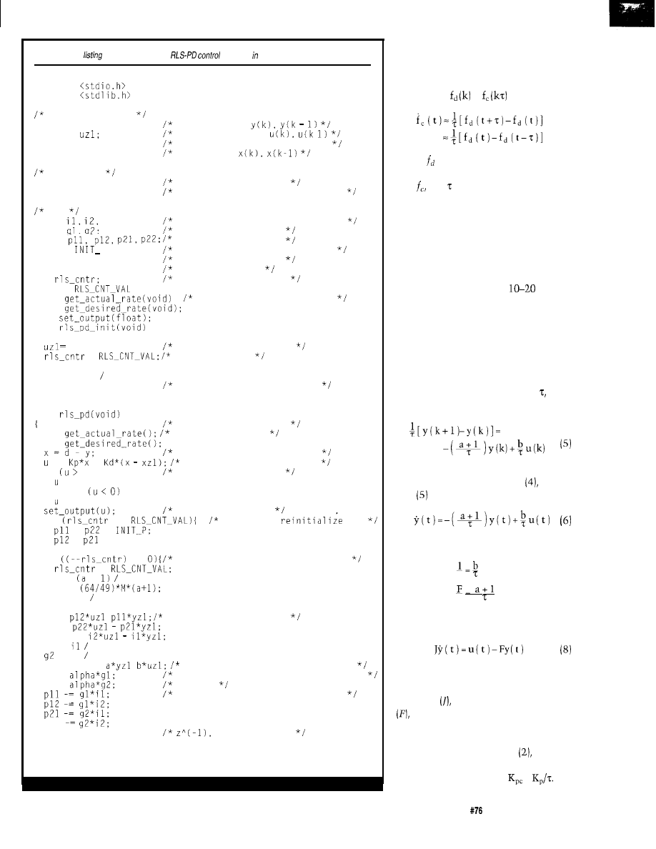
Listing l--This
shows the combined
algorithm C.
#include
#include
Run-time Signals
float y, yzl:
float u,
float d;
float x, xzl;
Controller
float Kp, Kd;
float M, coeff:
RLS
float
1;
float
float
#define
P
1000
float a, b;
float alpha:
int
#define
10
float
plant output
control signal
desired (target) plant output
rate error
PD control parameters
intermediate value for
K
D
and Kd
intermediate values for vector g
elements of vector g
elements of matrix P
estimate plant parameters, and
elements of vector w
estimation error
RLS iteration counter
called function prototypes
float
void
void
yzl =
xzl = 0;
clear run-time signals
=
initialize RLS
a = b = O ;
coeff = 64 49;
Kp = 1;
set arbitrary PD parameters
Kd = 1;
void
Eq. 2, Control Output
y =
get run-time data
d =
calculate rate error signal
+=
+
calculate control signal
if 1.00)
bound u to 0 to 100%
= 1.00:
else if
= 0:
set control output
if
==
if time to
RLS
=
=
=
= 0;
if
==
if time to calculate Kp and Kd
=
M = + b;
Kp =
Kd = M 7;
il =
Eq. 19, Gain vector g
i2 =
1 = 1 +
gl = 1;
= i2 1:
alpha = y +
Eq. 22, Estimation Error alpha
a +=
Eq. 21, Estimated Plant Parameters a
b +=
and b
Eq. 20, Inv Correlation Matrix P
p22
xzl = x;
Increment Time
yzl = y;
uzl = u;
I’ll convert equations
(1)
and (2) to
continuous time using these approxi-
mations:
=
(31
( 4 )
where is the discrete-time-sampled
version of the continuous-time vari-
able and is the sample period.
This approximation is not without
risk. If the sample period is too long
relative to the system’s time constants
or rise time, the first-derivative ap-
proximation is too inaccurate to be
useful.
I developed the algorithm on a sys-
tem with time constants
times
the sample period. In this case, the
magnitude and phase distortion intro-
duced by sampling was negligible.
The next step is to convert the
continuous-time versions of equations
(1)
and (2) to a single equation describ-
ing the response to a step input. By
subtracting y(k) and dividing by
equation
(1)
can be rearranged as:
Using the continuous-time approxi-
mations in equations (3) and
equa-
tion becomes:
J
J
(7)
then equation (6) simplifies to:
which is the familiar equation for a
rotating system relating the moment
of inertia the coefficient of friction
and the driving force (u) to rota-
tional speed (y).
To derive the continuous-time
approximation to equation
first
define the continuous-time propor-
tional control parameter
=
Circuit Cellar INK@
Issue
November 1996
43
Then, by rearranging and dividing by
equation becomes:
Using equations (3) and
equa-
tion (9) becomes:
(IO)
By differentiating equation (8) and
substituting (IO), we obtain the sec-
ond-order differential equation for the
combined plant-controller system:
The transient response of equation
(11)
to a step input needs to be ana-
lyzed to quantify the response time
and maximum overshoot. To analyze
the transient response, take d(t) to be a
unit step function and assume
= 0,
y’(O) = 0, and d(0) = 0.
Then, taking the
transform
of equation
(11)
and substituting:
D(
which is the
transform for a
step function of
1, we get:
Js
The interesting characteristics of
equation (12) can be gleaned by rewrit-
ing it as:
where the natural frequency
the
zero
and the damping coefficient
are defined as:
K
J
K
+F
For the controller to be self-tuning,
it must know what constitutes being
in tune.
The desired behavior of the plant
must be defined in terms of a set of
mathematical criteria that use data
available to the controller.
Three criteria to consider are the
type of response (underdamped, criti-
cally damped, or overdamped), the
damping coefficient, and the maxi-
mum overshoot to a step input.
If some overshoot can be tolerated,
the quickest convergence of the re-
sponse to the desired value can be
achieved with an underdamped sys-
tem, meaning the damping coefficient
is between 0 and
1.
A damping coefficient close to 0
yields a shorter rise time but greater
overshoot. With a damping coefficient
close to
1,
overshoot is small but the
rise time is longer.
Unless there are other system re-
quirements that affect the selection of
the damping coefficient, 0.5 is a good
compromise between reducing over-
shoot and shortening the response.
For a given damping coefficient in
an underdamped system, one more
factor affects the overshoot: the ratio
Issue
November 1996
Circuit Cellar INK@
between the zero (-c) and the real part
of the pair of complex poles
If the ratio:
is close to 1, the overshoot can be as
high as 70%. Larger ratios reduce the
overshoot, and by the time a = 4, the
overshoot is down to about 20%.
The minimum possible overshoot is
about 14% as a approaches infinite.
used
16 to keep overshoot below
20% allowing for some noise, but any
number greater than 4 is just as good.
By setting the damping coefficient
to 0.5, = 16 reduces to:
From this and the definition of
equation
it
follows that:
K
RLS ALGORITHM
Now that we can calculate and
from the plant characteristics and
what next? We know the sample
period and and are functions of a
and b, in equation (6).
So, if we can calculate a and b, we
are done. To do that, I returned to the
domain of discrete-time and borrowed
the RLS algorithm from DSP theory.
Least-squares is a method of finding
the best solution to an overdetermined
set of simultaneous equations. The
solution to the least-squares equation
is computationally expensive, involv-
ing n-dimensional matrix inversion
and multiplication, where is the
number of simultaneous equations.
Such a calculation may be beyond
the capability of a simple microproces-
sor. But, there’s a recursive solution to
the equation in which a simpler set of
calculations is performed for each
equation individually, and the results
from one set of calculations are fed
into the next.
To get the recursive solution, I need
to cast the problem into a standard
form known as the deterministic nor-
mal equation. First define the data
vector a:
and the estimated parameter vector w:
The performance measure used to
judge the estimated parameters is the
difference between the measured out-
put y(k) and the predicted output ob-
tained from the estimated parameter
vector in equation (1). This estimation
error e(k) is:
=y(
For a datastream of samples, we
get n instances of equation
which
can be cast into matrix form by defin-
ing the data matrix A:
Memory mapped variables
In-line assembly language
option
Compile time switch to select
805
1 or
Compatible with any RAM
or ROM memory mapping
Runs up to 50 times faster than
the MCS BASIC-52 interpreter.
Includes Binary Technology’s
cross-assembler
hex file
Extensive documentation
n
Tutorial included
Runs on IBM-PC/XT or
n
Compatible with all 8051 variants
508-369-9556
FAX 508-369-9549
q
Binary Technology, Inc.
P.O. Box
.
Carlisle,
MA 01741
Serial LCD
Modules
Want to spend time coding your application, not
debugging the LCD interface? We can help. We offer
that work off RS-232-style serial hookups.
Connect
ground, and serial data at 2400 or
9600 baud. That’s it!
Contact us or
download sample
user manuals,
catalogs, schematics
and other
from
our
archive.
serial-to-LCD
chips and boards
available at great
quantity discounts
Scott Edwards
ph: 520-459-4802 fax: 520-459-0623
Electronics
e-mail:
Circuit Cellar INK@
issue
November 1996
4 5
102
202
Figure 2-Control is sluggish for the
first ten samples until new control
parameters are
At the
second sfep input in d(k), the
controller is tuned.
Once a and b are estimated, the
control parameters and are found
from equations (7) and
which
reduce to:
7b
(23)
the error vector e:
and the measured data vector y:
1’11 simply assume that a miracle
curs and jump right to the solution.
First, I need to define one new
trix, two vectors, and a scalar. The
gain vector g is defined as:
In equation
the control param-
eters seem independent of the sample
rate, and in a sense they are. The
ple rate doesn’t directly contribute to
the control parameters, but a.different
sample rate would be made manifest
by different plant parameters a and
b.
From these definitions, e equates to:
where the inverse correlation matrix
is:
k ) = y ( k ) - a ( k ) w
( 2 0 )
In the least-squares method, the
square of e should be minimized. The
squared error function is:
The surface defined by this function
forms a bowl shape over the
a-b
plane.
The
a-b
coordinates under the lowest
point in the bowl define the point of
minimum error between the measured
output and the estimated output calcu-
lated from the estimated and b.
The estimated parameter vector w =
is evaluated by:
( 2 1 )
where the estimation error is:
The RLS parameter estimation
algorithm proceeds as follows. First,
equation
calculates the gain vector
At this point, the gradient of the
g, and equation (22) calculates the
error surface equals zero or:
estimation error
Using g and a, the estimated
rameter vector w is recursively up-
=o
dated in equation (21). In the last step,
equation (20) recursively updates
P.
which reduces to:
The algorithm is initialized at = 0
with
= 0, and
= where is
an arbitrary number greater than 1.
This is the deterministic normal
equation for least-squares parameter
estimation, and the solution w pro-
vides the necessary
a
and b.
Deriving the recursive solution to
equation (18) is a rocky trek through
linear algebra. But, now that the prob-
lem has been made to fit
wise into the standard form
there’s
Figure 3-At
the output
no need to reinvent the wheel. Instead,
overshoots. Again, the controller is
tuned at the second step input.
CONTROL ALGORITHM
Several issues need to be considered
before the RLS algorithm is ready. One
is the value of used to initialize
The only constraint on the value of
p-that the correlation matrix
has to stay invertible-is met by set-
ting to a number greater than 1
Otherwise, p’s value has little effect on
the results, except that a larger num-
ber results in faster convergence.
Another consideration is when to
recalculate the control parameters
and
The estimated plant parameter
vector w is inaccurate for a short time
after initialization. Control parameters
calculated from immature parameter
estimates don’t result in good control.
In a noisy system with a constant
target rate, the system reaches a steady
state with the error signal equal to
zero plus a noise component. In this
case, the RLS algorithm can get con-
fused and calculate plant parameters
that reflect the noise more than the
true plant characteristics.
You could skip recalculating the
estimated plant parameters unless the
target rate changes by an amount
0
105
202
502
46
issue
November 1996
Circuit Cellar INK@
nificantly greater than the magnitude
through the field to apply a constant
of the noise.
amount of fertilizer per unit area.
I found empirically that I can obtain
good results by running ten iterations
of the RLS algorithm before using the
estimated plant parameters to recalcu-
late the control parameters. Then, I
reinitialize the RLS algorithm and
recalculate the control parameters
after every ten iterations to keep up
with changing plant characteristics.
To complicate the issue, the ma-
chinery’s response changed with pow-
er-supply voltage, load, and usage as
bearings and gears jammed with fertil-
izer and dust. Also, the operators
wanted to use the same controller on
several different systems and to switch
from one to another at any time with-
out retuning the controller.
Listing 1 shows the combined
RLS control algorithm in C. The inter-
mediate vector i used in calculating
is also used in the calculation of
This works because i = PA in
so
=
which is what (20) needs.
The algorithm proved to be robust.
The controller could connect to a new
system and be tuned in l-2 s. And, the
tuning changed with plant characteris-
tics, keeping response consistent.
SYSTEMSUCCESS
Figures 2 and 3 show data obtained
from trial runs on the same system. In
each case, the target rate is 0.5 from
time 0 to time 2.5 s, after which it
goes to 0. At 4 s, it returns to 0.5 again.
In Figure 2, the control parameters
start at = 0.001 and = 1. The
result is a sluggish response for the
first second until the control param-
eters are recalculated. The response to
the input pulse at 4 reaches the tar-
get rate within 1 s, overshoots by about
and then settles down.
In Figure 3, the control parameters
start at = 1 and = 0.001, which
results in almost 50% overshoot in the
first second. But again, the response to
the input pulse at 4 is well-behaved.
COMPUTERS IN THE FIELD?
This algorithm allows the control-
ler to calculate automatically the pa-
rameters needed to achieve the desired
response. It produces a transient re-
sponse with specific characteristics,
but other characteristics can be cho-
sen. Different combinations of the
damping coefficient and the zero in
equation (13) simply change the con-
stants used in equation (20).
I implemented this algorithm on a
controller with a 12-MHz
clock. I was able to use a sample pe-
riod of 100 ms with plenty of time
available for other system functions.
The controller was used on a fertil-
izer spreader-literally, “in the
in which the fertilizer application rate
varied with the speed of the truck
Ken Baker works as a senior design
engineer at
a
d e v i c e c o m p a n y . Y o u m a y r e a c h K e n
at
The algorithm in 68HC 11 assembly
code, available on the Circuit Cellar
BBS, makes use of floating point
functions available on the Internet
at
is freeware
maintained by Motorola.
K . O g a t a , Modern Control Engi-
neering, Prentice Hall,
A d a p t i v e F i l t e r
P r e n t i c e H a l l , E n g l e w o o d
Cliffs, NJ, 381, 1986.
D i g i t a l C o n t r o l S y s -
S p r i n g e r - V e r l a g , B e r l i n ,
367, 1989.
68HCll
Motorola
MCU Information Line
P.O. Box 13026
Austin, TX 7871 l-3026
(512) 328-2268
Fax: (512) 891-4465
413 Very Useful
414 Moderately Useful
415 Not Useful
Data Acquisition
new Value-Line has
uncompromising design features
and high quality components at
prices below the low cost guys!
Just check out the specs:
5500MF
8 channels
A/D,
16
digital
Counter/Timer
H i g h S p e e d
8 channels
A/D,
DMA
M u l t i - F u n c t i o n D M A
5516DMA
16 channels 12-bit A/D,
DMA, 16 digital
H i g h R e s o l u t i o n
5500HR
16 channels
A/D,
DMA, 8 digital
learn more:
voice
800-648-6589
fax
web
www.adac.com
American Data Acquisition Corporation
70 Tower Office Park,
MA 01801 USA
Circuit Cellar
Issue
November 1996
47
David Rector
Getting Started With
Xilinx
Part 3: Hands-On Project-Implementation
fter you read this
series, I’ll bet you
discrete gate compo-
nents again. Erasable Programmable
Logic Devices
contain every
imaginable logic configuration bundled
into a single chip.
In Parts 1 and 2, Conrad and I de-
scribed the implementation of a design
into a Xilinx EPLD chip. If you’re on a
tight budget, skip the schematics in
Part 2, download the equation files,
and go on to implementation with
inexpensive implementation software.
In Part 2, I described the concept
and design of a timer/counter circuit
with microsecond accuracy that pro-
duced an analog waveform represent-
ing the counter’s current status. Many
applications use an analog waveform
(i.e., AIL code) to synchronize recorded
data, especially when many analog
waveforms are written onto a
chart recorder.
In this final installment, I’ll tell you
how to connect the chip into a circuit
that plugs into an IBM-compatible
computer. Then, you’ll be able to pro-
gram and use the timer/counter/wave-
form circuit. But first, you must select
the appropriate chip for the design,
CHOOSING SILICON
Speed isn’t a major concern-I need
l-MHz clock rates-but future expan-
sion to finer resolution waveforms
makes the
high speed essential
over
(up to 17 MHz for this
chip and up to 83 MHz with a faster
EPLD and less functionality in the
counter/address generator).
First, estimate the size of the chip.
Xilinx makes chips with several gate
densities and in various
from the XC73 18 (with 18 macrocells)
to the XC73144 (with 144 macrocells).
Count how many flip-flops you
need in your circuit. You need at least
one macrocell for each flip-flop or
output equation.
The AIL-chip design has 82
flops, so I chose the ‘73108 series. If
Photo 1-A complete waveform
card fits on a half-size PC card with plenty of room to
experiment.
48
Issue
November 1996
Circuit Cellar
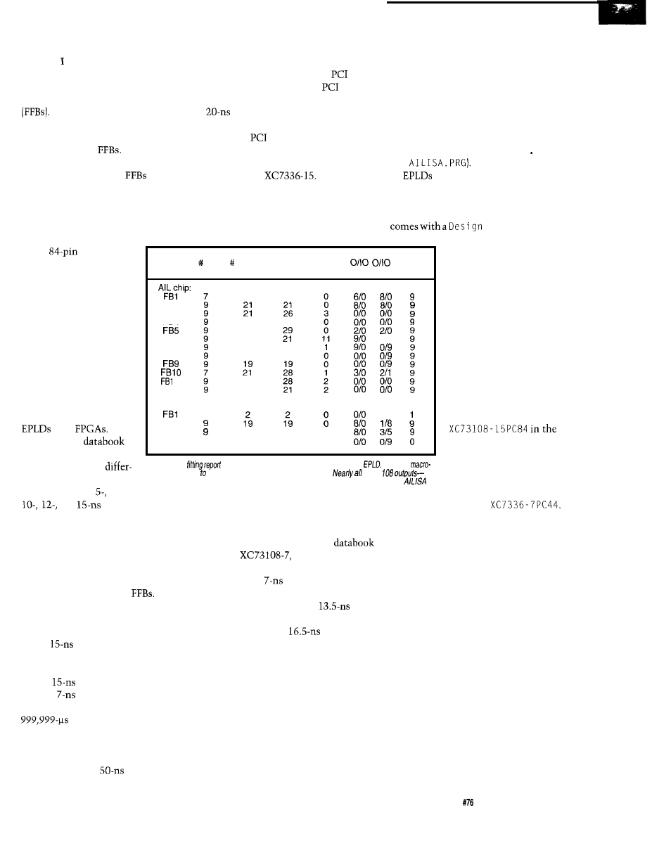
Xilinx’s implementation program are
you have complicated logic to imple-
ment, as did, some equations are split
into more than one macrocell.
Recall that
18
of the macrocells of
the ‘73 108 are in Fast Function Blocks
They operate faster but imple-
ment less logic (see Part 2, INK 75).
The XC73 18 and XC7336 are made
exclusively from
I chose the
XC7336 for the ISA interface because
of the high speed of the
and be-
cause of the number of I/O pins.
Finally, count the number of I/O, 0,
and I pins you need to get signals on
and off the chip. The AIL-chip design
requires few pins, so the
PLCC
package was
enough. If you need more
external pins, go to a
higher-pin package (e.g.,
the QFP 160).
FB2
FB3
delay for zero-wait-state communica-
tion with a 16-MHz bus clock. If you
ever wanted to hook up to a
inter-
face-which is easy with a
add-on
chip-you can’t tolerate more than
delay for 33-MHz operation.
Most of my PC-interface designs
target the
bus, so I required the
speed of the -7 grade XC7336. If you
stick exclusively to ISA, you can spend
less with the
Determining your design’s speed
can be tricky if there are multiple
macrocell levels. And, various signal
paths operate with longer or shorter
very good at describing the resources
needed and the resulting timing.
If cash is limited, bypass the sche-
matic-entry phase and download the
equationfiles(AILCHIP.XFFand
A I L I SA . X F F). Use Xilinx’s DS-550
design-manager software to generate
the programming files (A I LC H I P P RG
and
are programmedin three steps.
After the schematic is entered, the de-
sign is translated into an equation file.
The Xilinx stand-alone base system
Managerprogram
that performs this opera-
tion and is similar to the
DS-550 described in Part 1
(INK 74).
Part
of
of
Input
Signal
# of
S i z e
Name Outputs Lines Used Inputs Shared Pt Req. Avail. Factor
SELECTING SPEED
GRADE
To make a microsec-
ond counter, the chip
must operate at 1 MHz.
Predictable timing be-
tween inputs and outputs
is another advantage of
over
The Xilinx
lists timing specifications
FB4
FB6
FB7
FB8
1
FB12
AILISA:
FB2
FB3
FB4
24
24
19
19
2 i
21
20
26
19
19
019
2 0
21
0
18
18
0
0
0
0
019
The Windows-based
software is amazingly
easy to use. After specify-
ing the AIL-chip design
in New Project, click
Translate, andchoose
the XC7000 family.
The translation rou-
tine comes up with a
device-specification win-
dow. You must select
device specification for
the AIL-chip design if
you haven’t entered the
device in the schematic.
For the AILISA interface
for each of the five
Table l--The
describes how well your design fits into the
Unused
ent speed grades for their
cells
are the key how much room you have for expansion.
of the
each representing a single macrocell-are used in the All-chip implementation. The
chips. There is a 7-,
chip is only ha/f utilized, so you can improve performance by making a synchronous interface.
chip, use
Next, implement the equation file
for the chip. The implementation
routine fits the equations on the chip
and produces various performance
reports and timing files.
Try implementing the AIL chip
with different speed grades to see what
you get in the timing reports. Use all
the default options.
If you’re packing a lot of logic into a
chip, turn the timing optimization off
or your design won’t fit. Of course, you
can try having the timing optimization
on. Your design runs much faster, but
more resources are required.
If you’ve wired the chip and need to
freeze the pins, select Gu i de Des i gn
and choose the last version that uses
your pin configuration. Usually, you
can freeze the pins without much
trouble.
and
guar-
anteed delay from the fast clock input
to output valid.
Keep in mind that, if your output
equations get complicated, multiple
macrocells cascade with increased
delay. Some paths are faster if they
pass exclusively through
The AIL-chip design requires at
most 1000 ns from fast clock input
transition to outputs valid (count time),
so the
XC73108 is plenty fast for
my project. The exact timing specifica-
tions are in the timing report.
The
chip operates at 17 MHz,
and the
chip at 34 MHz. If you
simplify the circuit by cutting out the
reset and decade seconds
counters, you could scream at
83.3 MHz.
For the ISA interface chip, the bus
specifications list
maximum
delays, depending on how the fitting
software implements your circuit.
Look closely at the Xilinx
For the
if you use the fast
clock to drive a flip-flop, there’s a
maximum of
delay. But, the same
flip-flop driven with a regular input as
the clock line gives you a
de-
lay. For a pure logic equation with no
flip-flops, there’s a
delay from
input to output.
PROGRAMMING EPLDS
After your design is drawn into the
schematic-capture software or you
have written the equation files, you
can program the logic in the EPLD.
Once you have a general idea about
which chip to target, run Xilinx’s de-
sign manager to see how everything
turns out. The reports provided by
Circuit Cellar INK@
issue
November 1996
49
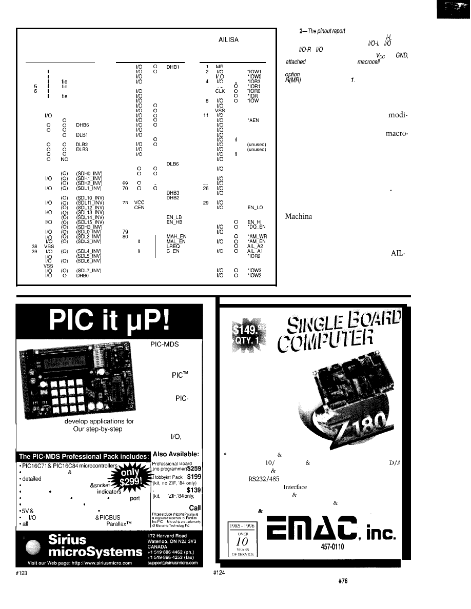
Table
lists each pin on the device,
and how it is used. Some abbreviations are = input
uses latch, I-R = input uses register,
= uses
latch,
= uses register, NC = not connected/not
a v a i l a b l e , t i e = u n u s e d
must be tied to
t o u s e d
gefthiswhenyouusethedrive
eset
AIL Chip
Pkg Pin Pin Pin
Pin Type Use Name
AIL Chip
Pkg Pin Pin Pin
Pin Type Use Name
Pkg Pin Pin Pin
Pin Type Use Name
1
MR
2
tie
3
tie
4
tie
7
8 VSS
9 CLK I
10 CLK 0
1 1
0
12
CLK
13
14
15
0
16
v s s
17
18
19
20
21
0
N C
22
v c c
23
24
25
26
27
v s s
28
29
30
31
32
33
34
35
36
37
40
(0)
41
42
(unused)
(unused)
(unused)
(unused)
(unused)
(unused)
45
0
46
MA10
47
MA1 1
48
0
MA12
49
v s s
50
0
MA18
51
0
MA2
52
0
MA17
53
54
MA19
MA8
55
MA20
56
MAO
57
MA1
58
MA3
59
0
MA16
60
VSS
61
MA4
62
MA6
63
0
MA7
64
VCC
65
0
0
66
67
DLB5
DLB4
68 0 0
DHB7
0
3
0
0
5
6
CLK
7
9
I
10
AD3
‘BALE
AD4
AD5
AD6
AD7
If you’ve made some major design
changes, conserve some pins by
fyingAILCHIP.GYD.Thistextfileputs
specific equations into specific
cells and directs I/O to specific pins.
Find the . GY D file you want as the
base and delete the equation lines and
any pin specifications that may make
it difficult to fit the new design. If
everything goes well, you’ll get a P RG
file with all the report files. Put the
chip in the ZIF socket of the Deus Ex
programmer and run X P GM.
The software provided with the
XPGM programmer needs to know
what kind of chip you’re programming
and the image file name. For the
chip design, use this command to
select the device, the package, and the
input file to program (see Part 1):
CLK
MA13
MA5
MA15
DLBO
I
12
I
13
I
14
I
15
I
16
17
tie
18
tie
19
20
I
21
v c c
DLB7
AS8
AS8
(unused)
(unused)
22
I
23 VSS
24
I
AS6
AS5
AS4
AD9
AD8
AD1
ADO
0
DHBS
DHB4
71
0
0
72
0
0
25
I
I
27
I
28 I
I
I
30
0
31
v s s
32
VCC
33
34
35
0
74
0
MA14
75
CEN
0
MA9
76
FOE I
77 FOE I
78
v c c
DIR
AD2
I
I A2
36
37
38
39
FOE
40
FOE
0
41
v c c
42
I
I
I
81
82 I
83
84 I
A l
43
44
43
44
The
is a
complete training
and development
environment for the
mid-range
microcontrollers.
Proven in class-
rooms, the
MDS lets you
learn to use and
r PIC microcontrollers
This board has the I/O and
Processor power to handle
demanding applications:
Serial, A/D, D/A, LCD,
Keypad, Real Time
Clock, EEPROM. and
Flash. This board has
got it all at a price that is
out of this world!
8
High-Drive Outs 16 Programmable Digital I/O Lines
* 8 Channels of
12 Bit A/D Optional 4 Channels of 12 bit
* 2, 16 bit Timers 2 optional 16 bit Counters
* Up to 3
Serial Ports
* Backlit Capable LCD
* Optional 16 Key Keypad Interface
* 1 Meg of Memory Space Total, 32K ROM 32K RAM Included
* Assembler Monitor Included, BASIC and Forth Optional
quickly and easily.
examples guide you from
simple programs through to keypad scanning, serial
LCD
display, A/D conversion, data logging, and interrupt routines.
EPIC Programmer PM assembler_
training manual with disk
in-circuit programming cable
ZIF socket buffered LED port
Hobbyist Board
2 X 16 LCD display 2 analog pots RS-232
no
256 byte serial EEPROM crystal/resonator socket
no programmer)
variable DC power supply AC voltage adapter
Teachers manual
all
pins on screw terminals
connector
code examples in Microchip and
syntax
8
618-529-4525 Fax
BBS 529-5708
P.O. BOX
2042, CARBONDALE, IL 62902
Circuit Cellar INK@
Issue
November 1996
51
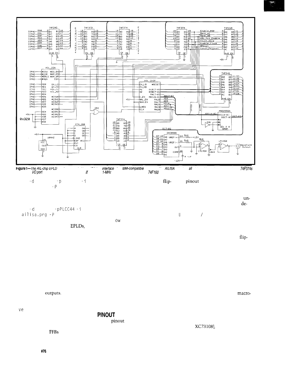
can De connected to an ISA-bus
of an
computer. The
chip does of fhe address decoding, and three
register fhe
data for three of the addresses.
you
get a
clock chip, you can cut fhe
decade counter.
used only fast clock lines to drive
the
report for each output and
flops. If any outputs are tristated, the
input.
enable line must be driven with the
It also lists the power and ground
special BUFFOE line.
lines and instructs you about the
If you have one or more regular
used lines. Some can be ignored
function blocks with fewer than nine
pending on how you set the
D r i v e
XPGM XC73108 PLCC84
ailchip.prg
For the AILISA chip, use:
XPGM XC7336
If you need to erase your
be
sure to erase the chip completely.
Incomplete erasure is not always indi-
cated by a blank check (see Part 1). It
is, however, indicated by erratic out-
puts [usually held high) or high run-
ning temperature (so hot you can’t
hold your finger on it).
FITTING REPORT
The fitting report describes how the
EPLD components are used. Each
block has nine
You can see
that nearly all of the outputs are used.
Your design doesn’t fit if you get
0 r
f 1 ow
function blocks in the fit-
ting report. If you can’t fit your design
into a particular chip, but you know
you’re close, try these tricks.
Underutilized
are solved by
paying strict attention to the rules. I
outputs used and few outputs on the
Over f 1 function blocks (i.e., the
total number of outputs doesn’t exceed
the available macrocells), you have too
many inputs on some equations.
You can split complicated equa-
tions in your circuit by placing a BUF
symbol between logic levels. This
technique increases delay time but lets
you pack more logic into the chip.
Table
1
summarizes the fitting
report for the AIL chip. Much more
information is provided, including how
macrocells were assigned to each equa-
tion. Any tricks the program played
while you weren’t optimizing perfor-
mance are also listed here.
REPORT
The
report is straightforward
(see Table 2). If you were careful about
labeling all of your nets (i.e., wires on
the schematic), these names appear on
n
u s
ed I 0
option, and some have to
be tied high or low.
The Master Reset line is always on
pin 1. This pin is useful if you’re short
on space-but be careful. If the
flops are reset by the same signal, you
can tie all of them low and use the
Master Reset line to reset the chip
instead of using macrocell resources.
This technique can significantly
reduce the amount of logic needed, but
depending on how the flip-flop is im-
plemented, it does different things. If
the flip-flop is part of an output latch,
it resets high. If it’s inside the
cell, it resets low.
Also, the Master Reset pin can take
a few milliseconds to complete the
chip initialization. Be prepared to wait.
Lastly, on chips like the XC7336
(not the
the Master Reset
pin can be used as a regular input sig-
nal pin. This must be specified either
52
Issue
November 1996
Circuit Cellar INK@
in the schematic or the implementa-
tion options.
TIMING REPORT
As far as your design’s performance is
concerned, the timing report is the most
important and most useful. It tells you if
your design will fly in the real world.
If your clock is going at 20 MHz and
the timing report says 1
maxi-
mum external clock rate, you better
use a faster chip. Otherwise, the be-
havior is unpredictable.
The timing report summarizes the
signal delays between input and out-
put pins, as well as delays from clock
edges to output valid.
If your design isn’t complicated or if
y o u u s e d t h e o p t i m i z e
tion during the implementation, the
timing report should merely be a copy
of the
timing specifications
for your chip. Otherwise, this report
shows how the split equations are
going to affect the timing delays.
For the AIL-chip design, I suffered a
significant loss in speed due to my
split equations, since my maximum
external clock rate is 17 MHz. With no
split equations, I’d expect 45 MHz.
The I/O delays also help assess how
the design performs in my circuit. For
example, a change at pad Al to select
the output byte takes, at most, 36 ns
until the output data bus is stable.
This is adequate for an ISA zero
state interface running at 16 MHz, but
not fast enough for a 33-MHz
bus
transfer.
BOARD CONSTRUCTION
Once your chips are programmed,
you can construct the PC board. rec-
ommend programming the chips be-
fore wiring the sockets because if you
have trouble implementing the design,
you may want to change the chip’s pin
configuration.
Figure 1 illustrates the schematic of
the completed circuit. The AILISA
chip
handles all of
the glue logic between the host com-
puter and the rest of the board.
A
acts as the data bus buffer,
another
buffers data to pro-
gram and reads the SRAM chip, and a
latches external inputs. Three
register control outputs, and a
third
reads back one of the
control registers.
One of the three output registers
controls AIL-chip operation, such as
latch request, reset, single stepping,
waveform-bank selection, and SRAM
programming. The second output reg-
ister drives the SRAM upper bits dur-
ing programming, and a third output
register drives external outputs.
I inadvertently discovered that the
are terrible at implementing
the registered output signals of the
Unfortunately, Xilinx doesn’t
provide enough ground pins, so occa-
sional spikes may occur on output
lines not registered by the fast clock
signals.
So, if any of your static outputs
(e.g., LREQ) drive a clock or enable
line which isn’t in sync with the fast
clock line of the signal source EPLD,
you may get an occasional erroneous
trigger on that line from ground spikes
within the signal source EPLD chip.
As a rule, I always register my static
output lines with something like a
and leave the signals governed
by the master clock signal to the EPLD.
As long as the output signals are syn-
chronous with the clock signal, I
haven’t had problems with the EPLD.
As you can see in Photo 1, the en-
tire circuit fits onto a half-size PC
board. Of 15 chips, 2 are used for exter-
nal I/O and are not needed for the AIL
circuit. The EPLD implementation
also requires fewer wires than discrete
components, which cuts down on
construction time and error.
WAVEFORM GENERATION
The address lines MAO-MA20 from
the AIL chip drive the address inputs
of an SRAM chip. In this example,
lines MAO-MA7 are ignored, which is
too fine of a resolution for right now.
So,
connect to address
lines AO-A12 of a 32-KB SRAM chip.
For my design, I use the upper two
bits of the SRAM address space (Al3
and A14) as waveform-bank storage.
You can select up to four different
waveforms by setting these bits of the
control I/O. The SRAM can be pro-
grammed by cycling through timer/
counter addresses with the single-step
control and writing to the SRAM.
You’ve
heard about the Dallas
and
805
compatible
CPU. It can really get the job
done fast, but you need to get
started right now. The 320SBC
features the ‘320 on a board that
is ready to go -- NOW.
32OSBC features:
. High speed 805 1 Instruction
set, executes instructions up
to 3X as fast as a standard
805 1 at the same crystal
speed.
l
Cost effective: $179 for the
50 development version,
$149 for the -10 OEM
version in single qty.
l
Two serial ports: RS-232
l
Optional 3rd RS-232 serial
port can be used to free both
the ‘320 serial ports for your
application.
l
On board monitor eliminates
the need for an ICE in most
cases.
l
Development tools for C
or ASM
l
Production ready design
Now
l
Special configurations
available that will reduce
cost and meet your specific
needs by including only the
features you need.
l
Compact size fits anywhere!
Equipment Corporation
566-1892
l
Fax: (619) 530-1458
Circuit Cellar INK@
Issue 876 November 1996
5 3
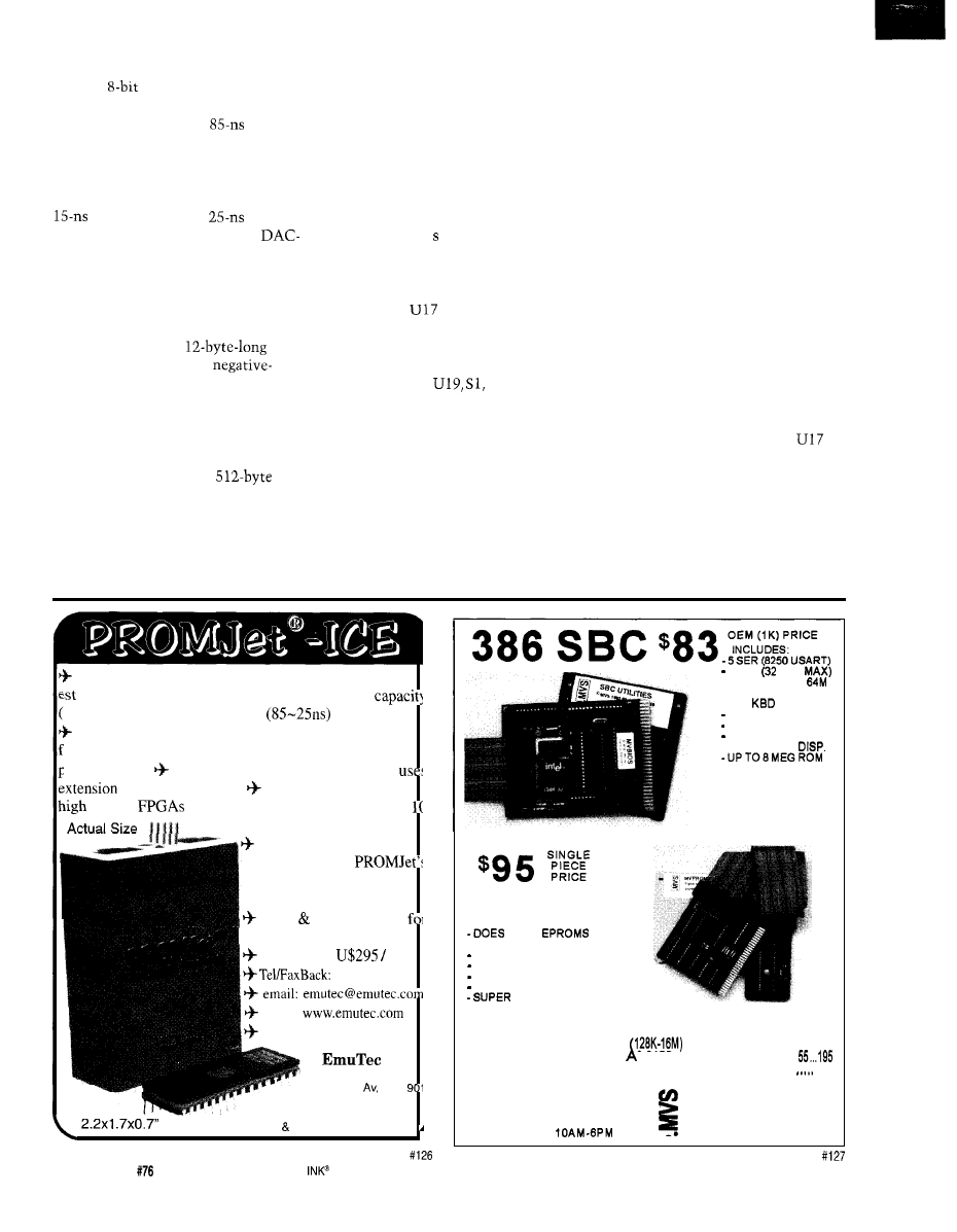
The data lines of the SRAM chip
drive an
DAC0808 and amplifier.
This example only updates the DAC
every 0.25 ms, so a slow
SRAM
and cheap DAC are adequate.
which is short or tall depending on the
state of S19.
For higher performance waveform
generation-one that updates each
microsecond, or up to 17 MHz for the
EPLD-use a good
SRAM
chip with a latchable DAC (e.g.,
0830) and drive the DAC latch with
the timer clock. For easier SRAM pro-
gramming, I added tristate controls of
the MA address lines on the AIL chip.
Another negative deflection is fol-
lowed by a positive deflection set by
S18.
This process continues until all
the second bit states are displayed
(excluding SO-S3).
Between each BCD number, a base-
line level separates seconds digits, and
between each 10 are more baseline-
level sequences. More specifically,
whenever SO or S3 is high, a baseline-
level sequence results.
The waveform file used to program
the SRAM has four 5
se-
quences. Sequence 0 is a
going deflection. Sequence 1 is a posi-
tive deflection with a small amplitude
hump, and sequence 2 is a positive
deflection with a tall hump. Sequence
3 is a baseline, flat level. The AIL code
is made up of 80 of these
sequences every 10 s.
Whenever
is low, we get a
negative deflection. Whenever U17 is
high, we get a positive deflection set to
the state of the seconds-counter bit
selected by U18,
and S2.
Look at the SRAM address-genera-
tor circuit to see how this is done. I
wrote a C program and a sample wave-
form file for you to test your circuit.
SOFTWARE TESTS BOARD
The SRAM address-generator cir-
This program resets your AIL chip,
cuitry determines the sequence display
loads the waveform file into the SRAM
order. Every
10 s,
a negative deflection
chip, continuously reads the AIL chip,
is followed by a positive deflection,
and displays the counter’s status. I list
the I/O ports you need and describe
each one in the program.
The program requires you to enter
the I/O port address of your board as a
parameter when starting the program.
The file
AI LWAVE. DAT
must be in the
same directory for the waveform to be
loaded.
To load the waveform into the
SRAM, the program cycles through the
microseconds counts in single-step
mode to generate the lower 10 address
bits. The upper three bits are set by
clearing bit 7 of the AIL control I/O
port which disables the upper three
bits from the AIL chip and drives them
independently.
Since the SRAM ignores the lower
8 bits of the microseconds, it writes a
value to the SRAM only after every
256 steps. Based on the state of
and the upper 3 bits of the SRAM ad-
dress IO port, a value from the wave-
form sequence is written to the SRAM.
Once the waveform is programmed,
the program’s second part continu-
ously latches, reads the AIL count
state, and calculates the time between
Ultra compact EPROM and FLASH emulator with high.
download speed (l-4 Mb/S), largest memory
l-32Mb) and fastest access time
in the industry
Other features include 3V target support, jumperless con
iguration, battery backup, 128 bit bus support and externa
lower supply. Fits directly into memory socket or
cable for flexibility. Compact design based or
density
and double-sided surface-mounted
layer PCB for added reliable operation
ICE option allows simulta-
neous access to
memory while target is run-
ning without waitstate signal.
Plug Play drivers
industry standard debuggers.
Priced from
MBit
206.337.0857
www:
Fax: 206.337.3283
Inc
Everett Mutual Tower
2707 Colby
Suite
Everett, WA 98201, USA
30 day money-back policy
Visa Mastercard accented
3 PAR
BITS
-32K RAM, EXP
-STANDARD PC BUS
-LCD,
PORT
BATT. BACK. RTC
IRQO-15 (8259 X2)
a237
DMA
a253
T M R
-BUILT-IN LED
-CMOS NVRAM
USE TURBO C,
BASIC, MASM
RUNS DOS AND
WINDOWS
EVAL KIT $295
UNIVERSAL
PROGRAMMER
a
M E
G
-CMOS, EE, FLASH, NVRAM
EASIER TO USE THAN MOST
POWERFUL SCRIPT ABILITY
MICROCONT. ADAPTERS
PLCC, MINI-DIP ADAPTERS
FAST ALGORITHMS
OTHER PRODUCTS:
8088
SINGLE BOARD COMPUTER . . . . . . . OEM $27 . . .
l 95
PC FLASH/ROM DISKS
16 BIT 16 CHAN ADC-D
. . . . . . . . . . . . . . . . . . 21 . . . . . 75
C CARD . . . . . . . . . . . . . . . . . . . . .
WATCHDOG (REBOOTS PC ON HANGUP) . . . . . 27
95
‘EVAL KITS INCLUDE MANUAL
BRACKET AND SOFTWARE.
MVS BOX 850
5
YR LIMITED WARRANTY
FREE SHIPPING
a
MERRIMACK, NH
HRS: MON-FRI
EST
(508) 792 9507
54
Issue
November 1996
Circuit Cellar
reads.
It does a line feed if something
is wrong with the time difference.
The AI L-RESET routine clears the
Master Reset pin and waits for the
LREQ latch to go low (i.e., not ready
on the UH14 line). This change indi-
cates that the chip is finished resetting
and can take as long as a millisecond.
NO MORE GUESSWORK
Now, you’re ready for your own
design. Once you get through your first
EPLD implementation, logic design is
a breeze. No more guessing about how
discrete components will interact.
If you perfect the art of synchronous
design, you’ll eliminate race condi-
tions. You can sit back in your most
comfortable chair and simulate the
design until you’re sure it works. Then,
burn the part and wire it up.
I think discrete logic gates will soon
be obsolete, so I hope you’re now feel-
ing comfortable with the next genera-
tion of logic design tools.
q
David Rector is a post-doctoral fellow
in the neuroscience program at UCLA.
He is continuing research on imaging
light-scattering changes in brain tis-
sue. You may reach David at
An AIL-chip test software sample
is available via the Circuit Cellar
BBS, the Circuit Cellar Web site,
and Software on Disk for this issue.
Please see the end of
for downloading and ordering infor-
mation.
Nu Horizons
31225 La
Dr., Ste. 104
Village, CA 91362
(818) 889-9911
Fax: (818)
Marvac Dow Electronics
2001 Harbor Blvd.
Costa Mesa, CA 92627
(714) 650-2001
Fax: (714)
DS-550, XACT
DSVL,
FPGA, EPLD Data Book
Xilinx Corp.
2100 Logic Dr.
San Jose, CA 95 124
(408) 559-7778
Fax: (408) 559-7114
Deus Ex
programmer,
Xilinx parts, and software
Corp.
701 Brooks Ave.
Thief River Falls, MN 56701-0677
(218) 681-6674
Fax: (218) 681-3380
EPLD programmer
Deus Ex
1377 Spencer Rd. W
Saint Paul, MN 55108
(612) 645-8088
Fax: (612) 645-0184
416
Very Useful
417 Moderately
418 Not Useful
56
Issue
November 1996
Circuit Cellar INK@
The Thrifty
Engineer
Daniel Nygren
eing thrifty
comes naturally to
was born tight as
a OS-mm pitch quad
flatpack, and this carries over to my
work as an engineer. This trait-and a
certain pack-ratish quality-comes in
handy when I’m cobbling together a
circuit to meet a deadline.
The project I’m about to share with
you is atypical for me because it in-
volves an IBM PC clone. Most hard-
ware types like myself sneer at PCs for
embedded systems because 80x86
assembly language is painful, the ISA
bus stinks, and MS-DOS is neither real
time nor multitasking.
These problems-and the fact that
the great unwashed think a PC can do
anything, and if it can’t, just get a
faster one-tend to make engineers
overlook PCs, if only at first.
REVIEW
Here’s the project in a nutshell. I
needed to take in a continuous stream
of asynchronous data at 4800 bps with
RS-422 levels, interpret it, and display
it on a number of standard composite
video monitors.
Well, I helped design a Motorola
68302
pro-
tocol conversion board, but it had no
video output. I considered taking the
data in on one RS-422 port on the
68302, formatting it, and sending what
was destined to be composite video
out RS-232 to an old Micromint Ter-
mite terminal or other RS-232-to-video
board. But, my cheaper instincts beck-
oned me elsewhere.
We had an abandoned 19”
mount IBM PC/AT clone lying around
our lab. It dawned on me that the IBM
PC/XT CGA cards had an RCA jack
that was an composite video output.
I
set up the little-AT-that-could, ripped
out its VGA card, and slapped the
CGA card into an
slot.
Warning-while genuine IBM PC/
have two
expansion slots,
not all AT clones have them. Most
CGA cards are of the full-length vari-
ety that won’t fit into a
slot
because the lower part of their circuit
board hangs down too low.
I wrote a program in Borland’s Tur-
bo C++ V. 3.0 for DOS after a cursory
inspection of its built-in communica-
tion routines. A tight loop of C code
continuously polled the communica-
tions port and printed the incoming
characters on the screen.
Well, the little AT couldn’t. It drop-
ped incoming characters regularly. Of
course, my final program didn’t have
to print to the screen continuously,
but I considered it a good benchmark
to see what the system could do.
REPAST
Over lunch at the local squat ‘n’
gobble, I whined to a couple engineers
about my predicament and how if IBM
had wanted PC design done right, they
should have asked me. After the
sided diatribe, one of my buddies said
he knew someone who used a PC to do
communications programs with some
canned C/C++ callable routines.
So, I hunted this guy down. He told
me he’d used Blaise Computing’s C
Manager with success. The
subroutines he purchased implement
an interrupt-driven communication
port buffer that stores up characters
until a main routine is ready for them.
Since he was done with the program, a
quick license check followed by eras-
ing the files off his hard disk meant I
was back on track.
If you’re still too cheap to spring for
a nice package like Blaise Computing
puts out, don’t despair. Similar subrou-
tines are available on the Internet.
All I needed was a way to get asyn-
chronous RS-422 data into my PC. I
contemplated using a couple of Maxim
MAX233 dual RS-232 transmitters and
receivers chips and some AMD
1 and
quad RS-422
line drivers and receivers on a spare
Issue
November 1996
Circuit Cellar
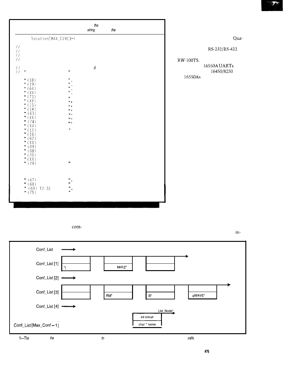
Listing l-An array of character
pointers is used to store string indicating the location of the handset on
each circuit. When a handsef comes off the hook, the
displays on appropriate conference.
char *
The string to be displayed when a circuit joins a conference
is held in this array. The length of the message in quotation
marks is fixed at 19 chars. Start with a space and put in 4
chars and a space for the number. This leaves 13 for the name.
(HANDSET NUMBER) NAME CIRCUIT
19 chars always!
//comment
DATA 3
DATA 3
RADAR 15
RADAR 14
CTRL 3
CTRL 3
RM 13
RM 13
RADAR 12
RADAR 16
CTRL 2
CTRL 2
EW OPS 1
PDPS
EW ACQ
EW PED
SAFTEY
CIRCUIT 2
SAFTEY
MIR 2
CIRCUIT 3
, //circuit 4
//circuit 5
//circuit 6
//circuit 0
//circuit 1
//circuit 7
//circuit 2
//circuit 3
//circuit 8
//circuit 9
//circuit 10
, //circuit 20
could pass information to each other
simultaneously.
GRUM
PES 2
MATS
a communication port. There had to be
a better way.
I just happened to get a catalog of
PC data-acquisition boards from
tech earlier that week. I paged through
until I found a nice
asynchronous communication board,
the
For a few extra bucks, I
could get it with
in-
stead of the common
chips.
The
have a 16-byte receive
FIFO that the Blaise Computing rou-
tines can take advantage of. I thought
I’d get an extra margin of safety in case
my code got more complicated than I
thought, so I sprang for the board with
the 16550s to make my major expense
for the project about $230.
RECAP
The data I was monitoring and
displaying came from an old custom
telephone switch that joined a large
number of handset circuits onto any
number of conference calls. The callers
However, without a way to monitor
//circuit 140
which caller was on which conference,
some users were concerned about
l/circuit 143
security. Anonymity encouraged mal-
contents to occasionally yell exple-
tives on certain conferences. Basically,
I was implementing Caller ID on our
system. The handset-site locations are
XT bus wire-wrap board to do a quick
But, it seemed kludgy to have the
given in Listing 1.
and dirty level conversion to RS-232.
RS-422 signals come into the PC, be
The switch was microprocessor
That way, I could use a standard
converted on my wire-wrap board, and
based. Earlier, I found the spot on the
munication port board.
looped back out, only to be taken in by
backplane where the CPU passed
[0]
NULL
NULL
6
20
60
15) RADAR 15”
“(20)
“(43) C&C LAB”
NULL
NULL
Figure
structure of array of
linked lists makes if easy build up, modify, and break down groups of phones in conference
Circuit Cellar INK@
Issue November 1996
59
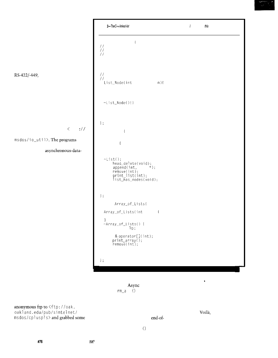
formation about who was on which
conference to the other system compo-
nents. I pulled out my handy-dandy
Hewlett-Packard 4952A protocol ana-
lyzer and monitored enough traffic to
figure out what was going on.
The HP-4952A is probably the most
useful piece of test equipment I have.
It displays, stores, and simulates mul-
tiple serial data protocols with RS-232,
and V.35 requirements
with its external interface pods.
If it worked at data rates above 64 kbps,
I’d probably marry it. Sure, it has its
faults. Like all HP equipment, it costs
too much. Still, you can pick up a used
one for less than half price at GE Rental or
Lease, RAG Electronics, or any com-
pany selling used test equipment.
If you are not thrifty, but deep down
stingy, try anonymous ftp to f t
p
oak.oakland.edu/pub/simtelnet/
comchkxx.zipanddlmxxx.zip turn
your PC into an
line monitor. While not the same as an
HP-4952, sometimes being thrifty
means not being too picky.
REPRISE
Flush with my knowledge of the
system, I started cranking out code. I
chose an array of linked lists with one
linked-list data structure for each con-
ference. I’d add and remove nodes
representing handset circuits from the
appropriate conference linked lists as
circuits joined, exited, or switched
conferences. When a circuit’s status
changed, I’d write it to the screen.
It took a while to shake the cob-
webs loose, but it wasn’t long before I
whipped some code out. Luckily, I
didn’t need a full-blown linked-list
implementation. I wrote member func-
tions to append a new caller, remove a
caller, and print out the callers on the
linked list (see Listing 2).
Figure 1 shows how the strings in
Listing
1
are held in the linked list.
The HP-4952A let me simulate the
system, so I worked out the bugs fairly
quickly. Thinking back, if I’d done an
linked-list routines, I’d have saved
about a week of coding and debugging.
Listing
class
definition for the linked-list c/ass wrote for program contains the
bare
minimum linked-list features /need.
class List-Node
Only the List class should be allowed to manipulate the
list nodes. So, make everything private, but allow the
List class access by making it a friend.
private:
friend class List;
A list node consists of a pointer to the next node, the
circuit number, and a pointer to the name in the location.
c, char *
next=NULL:
circuit=c;
name=n;
List-Node * next;
int circuit:
char * name:
class List
public:
List0
head=tail=NULL;
int
int
char
int
int
int
private:
List-Node * head, * tail;
class
public:
size)
lp=new Listlsizel;
delete II
iist
int
int
private:
List * lp;
The main routine was a different
from the s t r i
n g
h library to find the
story. Using the C
Manager, I
end-of-message byte in the buffer.
found a rd t
2
routine that read
I’d read a few of the previous bytes
in data until its fixed-length buffer was
to see which caller was being added to
full or it encountered a user-defined
or removed from which conference. I’d
terminating character.
update the linked lists and print the
I set up my program to give me a
data onscreen.
instant Caller ID!
buffer full of data whenever an
I remember going to lunch with the
message byte came from the system.
other engineers and saying perhaps I’d
Then, I used the s t r c h r
function
been too harsh when I ripped the PC’s
60
Issue
November 1996
Circuit Cellar
design to shreds the other day.
I
can be
rather magnanimous when I’m about
to complete a project in record time.
My head swelled to enormous pro-
portions as I hooked up the PC to the
switch and observed data appearing
onscreen. There were bugs to swat, but
everything was on schedule.
Of course, things were a bit more
complicated. I had to deal with a dread-
ed boundary condition. Suppose that
just before my buffer reached maxi-
mum length, the first few message
bytes came across, filling the buffer to
capacity.
The buffer didn’t contain my
of-message byte, which was at the
start of the next buffer. So, I had to
double buffer-that is, to maintain two
buffers to guard against my message
being split and lost.
If my message was cut in two, I
read the last few bytes from the previ-
ous buffer to reconstruct it. My code
became a bit messy taking care of this
contingency, but it worked fine.
RETRENCHMENT
One morning, disaster struck. Al-
though the evening before, things were
going smoothly, everything stopped
working. What had happened?
I stamped around for a while check-
ing cables and connectors. I gave the
PC a few three-fingered salutes (i.e.,
Ctrl-Alt-Del), all to no effect.
Then, I hauled out the HP-4952A to
see if I was still getting data. I
but it had changed! The end-of-mes-
sage byte was now
not
While I was beating my head on the
wall, one of the technicians who main-
tains the equipment wandered by to
make sure I wasn’t banging anything
he’d have to fix. After I explained the
situation, he said the end-of-message
byte probably changed because the
switch was a redundant system.
The switch was composed of two
identical switching sections. If an error
was detected in one, it automatically
changed to the other. He surmised that
the end-of-message byte indicated
which switch was the operational one
at the time.
To test his theory, he manually
changed the system to use its other
section. Sure enough, the
AN you can link together up to 250 of th
The
is:
fast-
A high speed
baud) multidrop
master/ slave
network
Flexible-
Compatible with your
microcontrollers
Reliable-
Robust 16-bit CRC and sequence
number error checking
Low microcontroller resource
requirements (uses your chip’s built-in serial
.
Friendly-
Simple-to-use C and assembly
language software libraries, with demonstration
programs
. Complete- Includes network software,
network monitor, and RS-485 hardware
.
is an asynchronous
adaptation of IEEE 1118
e-mail:
55 Temple Place
l
Boston, MA
l
Ph 617.350.7550
l
Fx 617.350.7552
“We’re impressed by the level of
documentation
by the readability of the code”
Ryan,
Inc.
high-quality
code, and excellent
technical support.”
L. Allen,
Inc.
“Personally,
the
Adaptation Kit and tool set very
straightforward to use, making
the BIOS development
process
easy.”
Chaplin, Software Engineer.
Includes our award-winning Run-From-Rom DOS
Includes Flash Disk for popular Flash parts
l
Over 300 easy configuration options
I
BIOS Kit includes full source code
l
Royalties
down
l
I
General Software’”
3 2 0
1 0 8 t h A v e .
S u i t e 4 0 0
W A 9 8 0 0 4
T e l : 2 0 6 . 4 5 4 . 5 7 5 5 F a x : 2 0 6 . 4 5 4 . 5 7 4 4 S a l e s :
E - M a i l :
Circuit Cellar INK@
Issue
November 1996
6 1
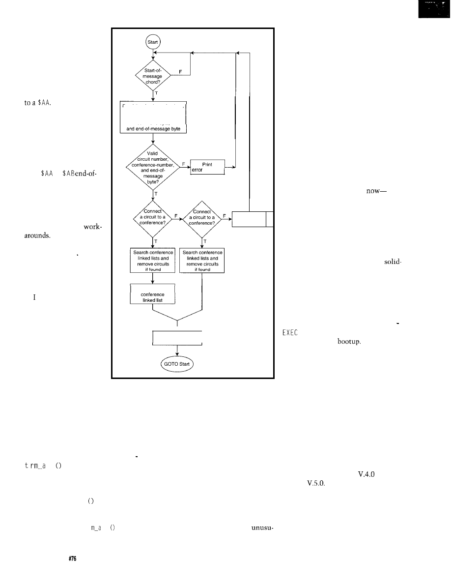
Figure 2-A flowchart can be
useful for figuring out how the
different strings in Listing 2 relate to
one another.
sage byte changed back
Now I
was in real
trouble because of my
choice of a PC for this
project. If I’d written all
the code myself in as-
sembler, I could just
have modified it to look
for a
or
message byte.
Read the circuit-number byte,
conference-number byte,
connect or disconnect
command byte,
But, I was using those
canned routines that
only allowed you to look
for one byte. My head
filled with devious
If I just cut a
trace on the mother-
board here and.. In
reality, my program’s
logic was doomed.
REPRIEVE
Append circuit to
think about work
when I run. My friends
say it’s because anyone
running that slowly has
plenty of time to pontifi-
cate between each step.
As I pounded the pave-
ment, I concentrated on
the problem of the mul-
tiple end-of-message
bytes.
Print each conference
and their circuits
Well, there are two ways to deal
with any problem-either do it or
don’t. The solution here was not to
deal with the end-of-message bytes but
with the start-of-message byte.
terminal instead of a start-of-message
character. As shown in Figure 2, this
solution reduced my program size and
simplified my logic immensely.
The start-of-message byte didn’t
change on the messages. So, I decided
to look for it instead. I set up the rd
2
routine to read in charac-
ters until a start-of-message byte was
RELIABILITY
This PC’s reliability did concern
me. It needed to run 24 hours a day,
seven days a week. It was no ordinary
PC sitting on a desk, only used during
message
error message
encountered and then read in the next
business hours. I attacked this problem
few bytes of the message.
by trying to avoid the frailties that
No more s t r c h r
routine, no more
most often cause PCs to malfunction.
boundary conditions and double buffers.
Certain PCs seem to go through the
Why didn’t I do this in the first place?
batteries that back up their CMOS
Perhaps the r d t r
2
routine
memory-contained setups at an
made me feel obligated to read in a
ally high rate. If you haven’t had the
pure joy of trying to figure out what
disk drives (and their corresponding
drive-type numbers) are on a PC with a
dead battery, you haven’t lived yet.
If you can’t stand the excitement,
buy a rechargeable battery instead of
standard lithium batteries. I bought
the Batpac from Industrial Computer
Source.
These batteries take power from a
disk-drive power connector to continu-
ously recharge the backup battery. In
case you don’t have a spare power
connector, they provide another con-
nector so you can daisy chain the pow-
er on to your disk drive.
However, I suggest you grab a magic
marker and write the drive-type num-
ber on the disk itself. Do it
you’ll thank me later.
Another component somewhat
prone to failure is the hard-disk drive.
Hard disks have come a long way, but
I’ll wager that something that doesn’t
spin at 2000 rpm lasts longer than
something that does.
I spent some time researching
state disk drives and putting my pro-
gram into EPROM or flash memory. I
finally decided to go with something
extra thrifty-a floppy-disk drive.
I yanked out the hard drive, made a
bootable floppy disk, copied my pro-
gram to the floppy, and had the AUTO
. BAT file run my program from
the floppy disk at
Sure, a flop-
py disk spins, but since my system is
rarely rebooted, the disk is seldom
accessed.
Of course, you can only do this for a
program that fits on a floppy disk and
doesn’t write much of anything to it.
But, these are the types of simple em-
bedded designs I am targeting.
To be legal, you must purchase a
copy of MS-DOS for each PC running
MS-DOS. A thrifty solution is to use
one of your old copies of MS-DOS (or
PC-DOS, DR-DOS, etc.) laying around.
Anyone can scrape up an unused
copy of DOS V.3.3, DOS
(yikes!),
or DOS
Most of the features
added to DOS over the past few years
aren’t needed by an embedded system.
One last unrelated hardware problem
arose from using a PC as a stand-alone
system-the keyboard. Nobody wants a
keyboard around, cord in a tangle, falling
62
issue
November 1996
Circuit Cellar INK@
Embedded PC with Foating
Point, Ethernet Super
VGA;
x
popular
board microcomputer.
Compact
a n d h i g h l y
rugged, it boasts a
CPU clock frequency and a full
8K Cache with Floating Point.
W ith more performance and all
t h e p o p u l a r f e a t u r e s o f i t ’ s
predecessor, the
offers
the OEM the greatest flexibility in
the smallest form factor.
Chip Set at 25 MHz
*Built-in 8K Cache Floating Point
*Local Bus Super VGA Video/LCD
to
DRAM
to
Flash” with TFFS
Ethernet Local Area Network
or ISA Bus compatible option
x 4” format
watts power consumption at t5 volt
For more information call:
Fax: 416-245-6505
Internet: www
125 Wendell Ave.
Weston, Ont.
off shelves, tempting the button pusher
in all of us to try a few keys.
Fortunately, it wasn’t a real prob-
lem. My BIOS setup let me ignore
keyboard errors and thus operate with-
out a keyboard.
Most newer
have this fea-
ture, but since this article is about
getting some use out of forgotten PCs,
here’s a solution. Vetra Systems pro-
duces a little box called Eliminator
that plugs in the keyboard port in
place of a true keyboard, fooling a
system into thinking one is present.
RELAX
The little-AT-that-could has been
in operation for over a year with no
difficulties. I socked away a spare CGA
card and an interface card, so in the
unlikely event of a catastrophic fail-
ure, we can drag a PC off a desk and be
up and running again in a matter of
minutes.
Since most of our technicians are
familiar with PCs, I won’t necessarily
receive an emergency call to come in
and direct resuscitation efforts if some-
thing fails. All in all, I’m pleased with
the outcome. In the proper situation,
with the proper precautions, PCs can
become part of an effective embedded
system.
Daniel Nygren received his BSEE from
Clemson University and his MSEE
from the University of Texas at Aus-
tin. His interests include real-time
fault tolerance, aircraft command and
control systems, and tactical digital
information links. You may reach Dan
at
Files are available via anonymous
asyncnch.
zip,ibmcom_c.zip,and
tcommxx. zi p are similar rou-
tines. The libraries
i bxx.
zipandcom_int.ziparealso
routines to try. Files are also
available from the Circuit Cellar
BBS and Software on Disk for this
issue. See
in this
issue for more information.
MAX233 Dual RS-232 transmitters
and receivers chips
Maxim Integrated Products
120 San Gabriel Dr.
Sunnyvale, CA 94086
(408)
Fax: (408) 737-7194
and
quad
RS-422 line drivers and receivers
Advanced Micro Devices
P.O. Box 3453
Sunnyvale, CA
(408)
protocol analyzer
Hewlett-Packard
Portable Computer Division
1000 NE Circle Blvd.
Corvallis, OR 97330
(503) 75 7-2000
C
Manager
Blaise Computing, Inc.
819
Way
Berkeley, CA 94710
(215) 443-9705
Fax: (215)
Inc.
662 Wolf Ledges Pkwy.
Akron, OH 44311
(216) 434-3154
Fax: (216)
Turbo C++
Borland International Inc.
1800 Green Hills Rd.
Valley, CA 95067
(408)
Eliminator
Vetra Systems Corp.
275-J Marcus Blvd.
Hauppauge, NY 11787
(516) 434-3185
Fax: (516) 434-3516
Batpac
Industrial Computer Source
P.O. Box 910557
San Diego, CA 92191-0557
419 Very Useful
420 Moderately Useful
421 Not Useful
66
Issue
November 1996
Circuit Cellar INK@
DEPARTMEN
From the Bench
Silicon Update
Tools
Part
1:
Schematic
the Proverbial
Electronic
Napkin
Jeff Bachiochi
From grocery-store receipts, ticket
stubs, and the morning paper to bank
statements, office memos, and sales
reports-it’s extremely difficult to give
up the security of a physical copy of
each and every transaction.
It’s not that we haven’t made prog-
ress. Computers store more informa-
tion. But, it’s comfortable holding
paper instead of a piece of magnetic
medium which, although it contains
more information and is written in a
global language, can’t be directly inter-
preted by a human.
I’ve come to appreciate the benefit
of a word processor over typing re-
ports, correspondence, or a monthly
column. The ability to create, edit,
store, recall, view, and print saves
hours of unnecessary typing. At my
hunt-and-peck typing rate, those hours
add up. The first time I needed to
change some correspondence, I saw the
light.
In engineering, we all have stories
of creating the schematic for a new
product or solution on a dinner nap-
kin. But, just imagine opening a user
manual only to find a copy of the nap-
kin reproduced complete with food
stains. To avoid this kind of embar-
rassment, schematics of yesteryear
were painstakingly redrawn using a
full-size drafting board.
CAD
Such labor-intensive work has been
unnecessary for many years now,
thanks to a wide selection of
68
Issue
November 1996
Circuit Cellar INK@
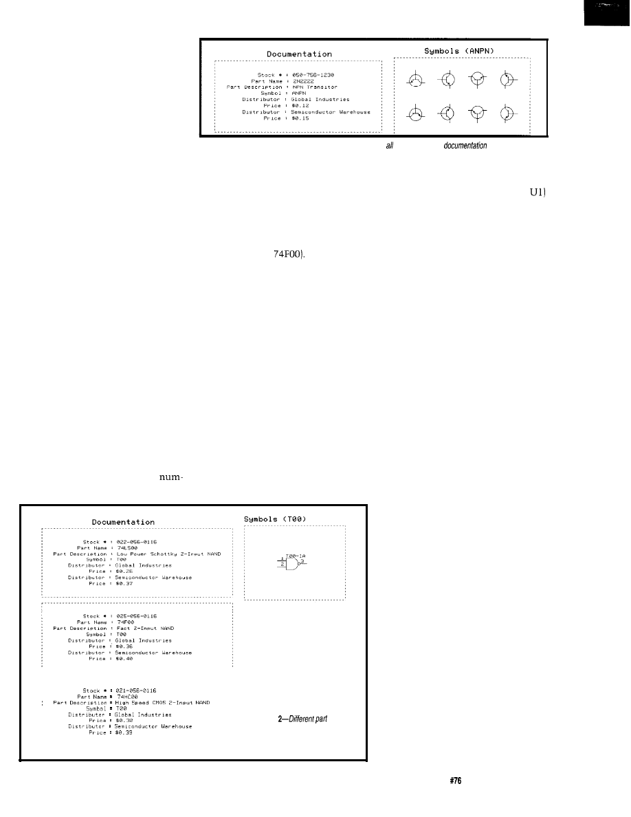
matic-capture packages. The best part
is that you don’t have to spend big
bucks to get professional results.
Although these programs differ in
look and feel, y need to know the three
basic sections-parts library, drawing
editor, and postprocessor-to use the
programs effectively.
The parts library is a database of
shapes or symbols and associated part
information. The drawing editor dis-
plays and handles the parts’ symbols
and their interconnections. The post-
processor creates documentation from
the drawings and database.
Figure l-Although many views of a part might be used, they share the same
which symbol the drawing editor uses
to define its physical appearance on
the schematic page.
As shown in Figure 1, several orien-
tations of the same part are available.
Parts individually defined in the docu-
mentation may share the same symbol
(e.g., 74LSO0 and
Figure 2
shows how parts can have different
documentation but the same symbol.
Symbols, too, take on specific infor-
mation when used. Both the part type
(e.g., 74LSOO) and designation (e.g.,
are attached during placement.
You can see there’s more to the
schematic-capture library than just a
bunch of pictures. The library database
may be divided into many smaller
libraries sorted by device type (e.g.,
linear, digital, memory, processors,
etc.] or manufacturers (e.g., Motorola,
National, Siemens, etc.)
Let’s look at each of these in detail.
PARTS LIBRARY
Just as books are stored on shelves
in a public library, all electronic parts
are stored in a repository of equal pro-
portion. The number of predefined
parts in the parts library varies based
on the cost of the package.
include a device name and stock
ber, where it can be purchased, and
The higher-priced packages might
include whole libraries from individual
manufacturers. But, even minimal
libraries have many standard parts.
Each part in a library is made up of
at least two pieces-the documenta-
tion and the symbol. Figure 1 shows
the documentation and symbols one
might have for a transistor.
The documentation contains infor-
mation describing the device. It might
The parts symbol stored in the
library reflects the part’s appearance
on the page and the electrical informa-
tion associated with each pin of the
device. This information describes the
function of each device pin and is used
in postprocessing for error checking.
where the part’s specifics are entered
when it is used in a drawing.
Associated with each pin is a point
on the symbol where any external
connection must be made to connect
to the device. This point is usually the
end point of what it would look like
on the symbol’s component pin.
To manage the library’s size, parts
can have generic names like “resistor,”
Figure
families
may share the same part
symbol.
DRAWING EDITOR
Substitute the computer screen for
a dinner napkin and use the drawing
editor to place parts on a page. To do
this, the part name is entered and the
parts library is searched.
If a match is found, the symbol for
that part is placed on the page. You
can move the symbol around the page
and choose the necessary orientation.
Parts should be placed in a logical
fashion. Generally, circuit flow moves
left to right (i.e., inputs on the left and
outputs on the right). Or, start with
the largest part first (e.g., a processor]
and place the smaller ones around it.
Large circuits that don’t fit comfort-
ably on a single page can be broken
down into separate pages by function.
Don’t crowd too many parts too close
together. Think of the circuitry as a
block diagram. Place the parts which
make up each block on a separate page.
But, parts alone do not a schematic
make. Connections between parts
create a circuit’s character. All connec-
tions in a single path make up a net.
A net is created when you connect
two or more part symbols’ pins to-
gether by drawing a line (i.e., wire)
between them. For identification, each
net is given a name either by the user
or automatically by the program.
It’s almost impossible to draw a
schematic without crossing any lines.
Circuit Cellar INK@
Issue
November 1996
6 9
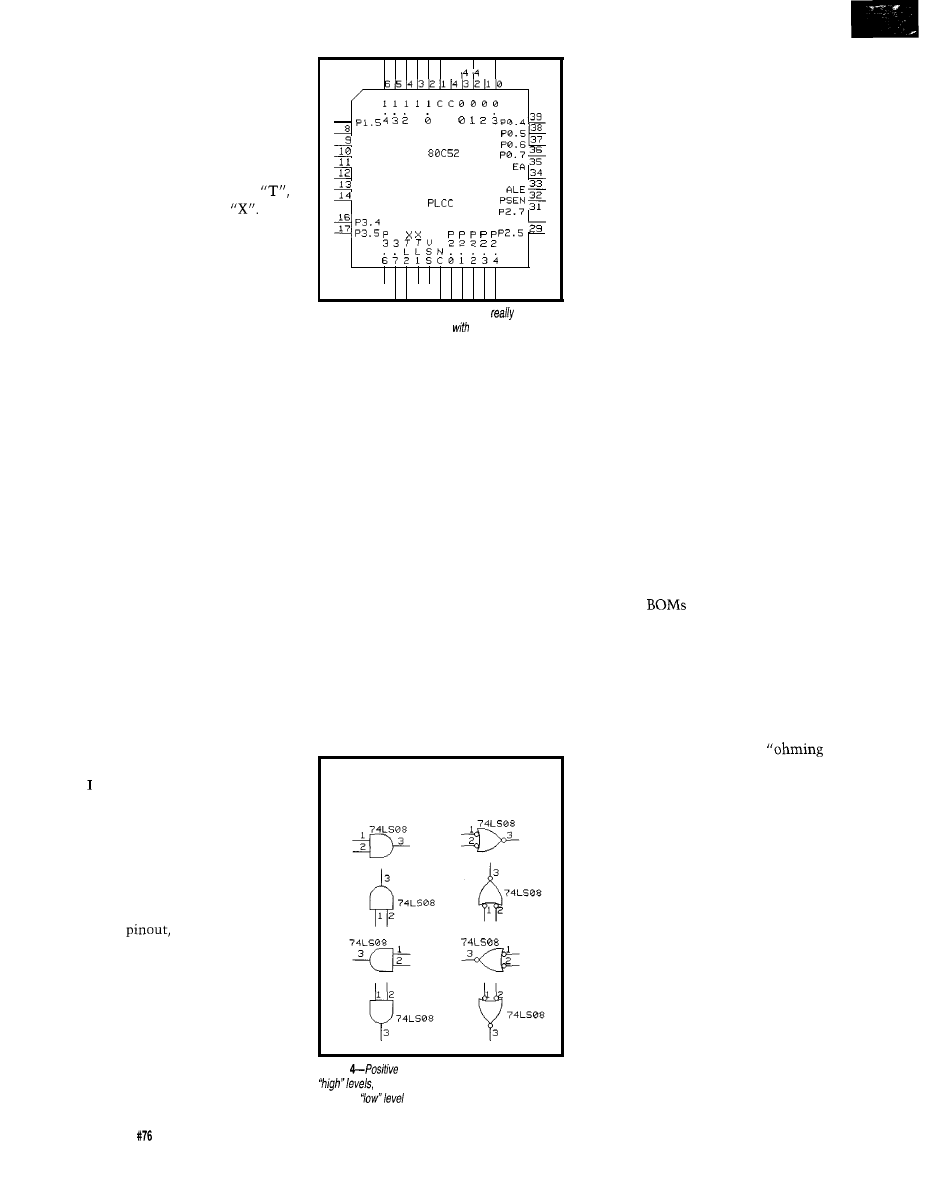
Crossing lines are considered con-
nected when a dot (which looks like a
blob of solder] is placed on the point of
intersection.
To eliminate the possibility of mis-
understanding when lines are crossing
or connected, follow this simple rule: a
connection is always shown as a
and two lines crossing is an
When many connections must be
made between parts, the web of indi-
vidual lines becomes confusing. A bus
connection simplifies the page.
Think of each connection or line as
a wire and a bus as a multiconductor
jacketed wire (drawn as a wide line).
Each individual wire can enter or exit
the jacket at any time. When it does, it
must be identified.
In reality, color coding each wire
identifies it. On the schematic page,
labels are used. Colors can be labels,
but signal names make more sense.
Schematic pages with a single draw-
ing name are all part of the same cir-
cuit, and any pages with the same net
label are connected. Just as too many
individual lines can be confusing on a
schematic, a bus containing all con-
nections can be equally confusing.
I use multiple buses. For example,
when drawing a microprocessor, I like
to use three buses-an address bus, a
data bus, and a control bus. Since the
signals within each bus are related, it’s
easier to visualize the flow.
A good drawing editor not only
functions as a schematic drawing and
editing tool, but it also creates and
maintains your parts library. Every
time draw a new schematic, there’s
at least one new part. The editor lets
me easily document the new part and
then define a symbol by drawing it.
You can design the symbol using
the normal left-to-right I/O flow or be
creative. You can draw the symbol the
way the part physically appears (e.g., a
PLCC chip
as shown in Figure
3). Doing this gives the technician
probing the PLCC socket a visual cue
to where each signal can be found.
After the symbol is drawn, its pins
(i.e., connections) must be defined.
You must define external connections
to the part and the internal functions
of the pin within the device. The pin
might be classified as an input, output
4
P P P P P N U P P P P
i
7
c
.
.
P 1 . 6
P 1 . 7
RST
P 3 . 0
NC
P 3 . 1
NC
P 3 . 2
1 5 P 3 . 3
3 0
P
P 2 . 6
1 1 2 2 2 2 2 2 2 2 2
8 9 0 1 2 3 4 5 6 7 8
Figure 3-The processor is shown as it
looks,
making it easy to troubleshoot
a scope probe.
(i.e., open collector or tristate), bidirec-
tional, or don’t-care.
Using positive and negative logic
forms clarifies a circuit’s function. All
logic can be described using both posi-
It’s advantageous to create special
versions of part symbols for a particu-
lar drawing. Programmable devices can
tive and negative as shown in Figure 4.
to be customized according to use.
Positive logic describes the logic
function based on the high logic level
of the input, as in
“1
AND
1”
(equals
1).
The same AND gate described in
negative logic is “0 NOR 0” (equals
1).
When describing the control logic of a
logic-low chip select, negative logic
improves clarity.
POSTPROCESSING
If you use a schematic for documen-
tation only, you may not need to use
Positive
Negative
Logic
Logic
Figure
logic describes a function using
while negative logic describes a function
based on
input.
postprocessing. However, it points out
drawing errors, produces a bill of mate-
rials, and creates links to other CAD
programs.
The postprocessor uses the informa-
tion contained in the parts symbol to
detect potential errors. Each net is
analyzed to determine whether certain
rules have been broken.
The error report points out nets
with no driving source (i.e., floating),
more than one permanent driving
source, single pins with labels, and
nets with multiple labels. The postpro-
cessor also points out parts with the
same parts designator or that use a
gate within a package more than once.
To actually build the circuit you
have drawn, you’ll need a bill of mate-
rials (BOM). The postprocessor lists all
the parts used in your drawing.
Naturally, the postprocessor can’t
locate a logic error. That’s left up to
your engineering skill. (You can al-
ways turn to a timing analysis program
to debug the logic.)
Quantities, part names, stock num-
bers, manufacturers, distributors, pric-
ing, and the like can be pulled from
the parts library’s documentation sec-
tion. Most
can be customized to
your own parameter format.
To physically wire a prototype, the
postprocessor can prepare a wire list.
The wire list is a human-readable list
of nets. Wire wrapping-popular for
many years-used the wire list to
daisy chain all the connections within
a net. The list is also good for
out” a finished prototype to ensure no
connections are left out.
A postprocessor can also produce a
machine-readable list of nets. The net
list is all a PCB program needs to en-
sure connectivity in creating a PCB
layout.
The catch is that every PCB-layout
program requires a net list in its own
format and every schematic drawing
package creates its own net list format.
You’d think these companies could
agree on a standard format, but most
won’t accept another format directly.
Fortunately, many packages include
pin/net conversion programs to con-
vert their format to one used by other
PCB-layout packages. Companies with
a complete line of CAD aids don’t
70
Issue
November 1996
Circuit Cellar INK@
Powerful Tools,
Reasonably Priced.
Supports EPROMs to 128K x8
to
(1 MEG)
Supports EPROMs to
x8
to
(4MEG)
l
Powerful PC software
l
Full screen command line
modes
l
Supports all data formats
l
Software configurable
access time standard,
optional
32
PIN PLCC adapters
s.
version, operates at both
and 5V
l
Memory backup feature
l
High-speed downloading (LPTI-3) with
error checking and correction
l
Non-intrusive CMOS LP design
l
Chain up to 8 units -any configuration
l
Compact size in hard protective case
l
1 year warranty free software upgrades
l
Discounts on
units
SDI
S C A N L O N
D E S I G N
INC.
5224
Blowers St. Halifax, NS Canada
TEL: 902 425 3938 FAX: 902 425 4098
T o l l
F r e e
i n N o r t h A m e r i c a
800352 9770
usually require conversion between
packages.
If you’re using one company’s sche-
matic-drawing package and another’s
PCB-layout package, make sure a con-
version program is available.
THAT’S NOT ALL
Since these programs enable you to
draw lines and generate text, the sche-
matic-capture program can be used to
create block diagrams and flowcharts.
Although you can’t do timing analysis,
you can draw timing diagrams.
Many libraries contain physical
symbols of parts in relation to other
parts. You can experiment with parts
placement on a pseudo-PCB drawing
which guides the PCB-layout artist.
A lot of information cannot be
transferred in a simple net list (e.g., the
importance of placing the decoupling
capacitors near the
The net list
only indicates that decoupling capaci-
tors and
are connected in parallel.
Once a schematic is drawn, I’m
usually asked how tightly I can cram
these parts together. Using the sche-
matic package for parts placement
offers an early estimate of board space
and passes placement information on
to the PCB-layout engineer.
CHECK, PLEASE
Next time you’re at lunch, save the
napkins for the spaghetti sauce on
your shirt. And when you’re back at
the office, get comfortable with your
schematic-capture package.
Tune in next time for the basics of
PCB layout and what’s necessary to get
that circuit fabricated.
Bachiochi (pronounced
AH-key”) is an electrical engineer on
Circuit Cellar INK’s engineering
staff.
His background includes product
design and manufacturing. He may be
reached at
Tango, PCAD
ACCEL Technologies, Inc.
6825 Flanders Dr.
San Diego, CA 92121
(619)
Fax: (619)
Eagle
Computer, Inc.
801 S. Federal Hwy.
Delray Beach, FL 33483
(561) 274-8355
Fax: (561) 274-8218
Corp.
20 Fairbanks
Irvine, CA 926 18
(714) 770-3022
Fax: (714)
Harmony
OHIO Design Automation, Inc.
Technology Park
78 Pine St. Ext.
Nashua, NH 03060
(603) 598-2525
Fax: 603) 598-2626
9300 SW Nimbus Ave.
Beaverton, OR 97008
(503) 671-9500
Fax: (503)
PADS Software, Inc.
165 Forest St.
Marlboro, MA 01752
(508)
Fax: (508) 485-7171
Protel
Protel Technology
4675 Stevens Creek Blvd., Ste. 200
Santa Clara, CA 9505 1
(408) 243-8143
Fax: (408) 243-8544
Wise Software Solutions
8285 SW Nimbus Ave., Ste. 191
Beaverton, OR 97008
(503) 626-7800
Fax: (503) 520-I 759
Zuken-Redac, Inc.
238 Littleton Rd., Ste. 100
Westford, MA 01886
(508)
Fax: (508) 692-4725
422
Very Useful
423 Moderately Useful
424 Not Useful
72
Issue
November 1996
Circuit Cellar INK@
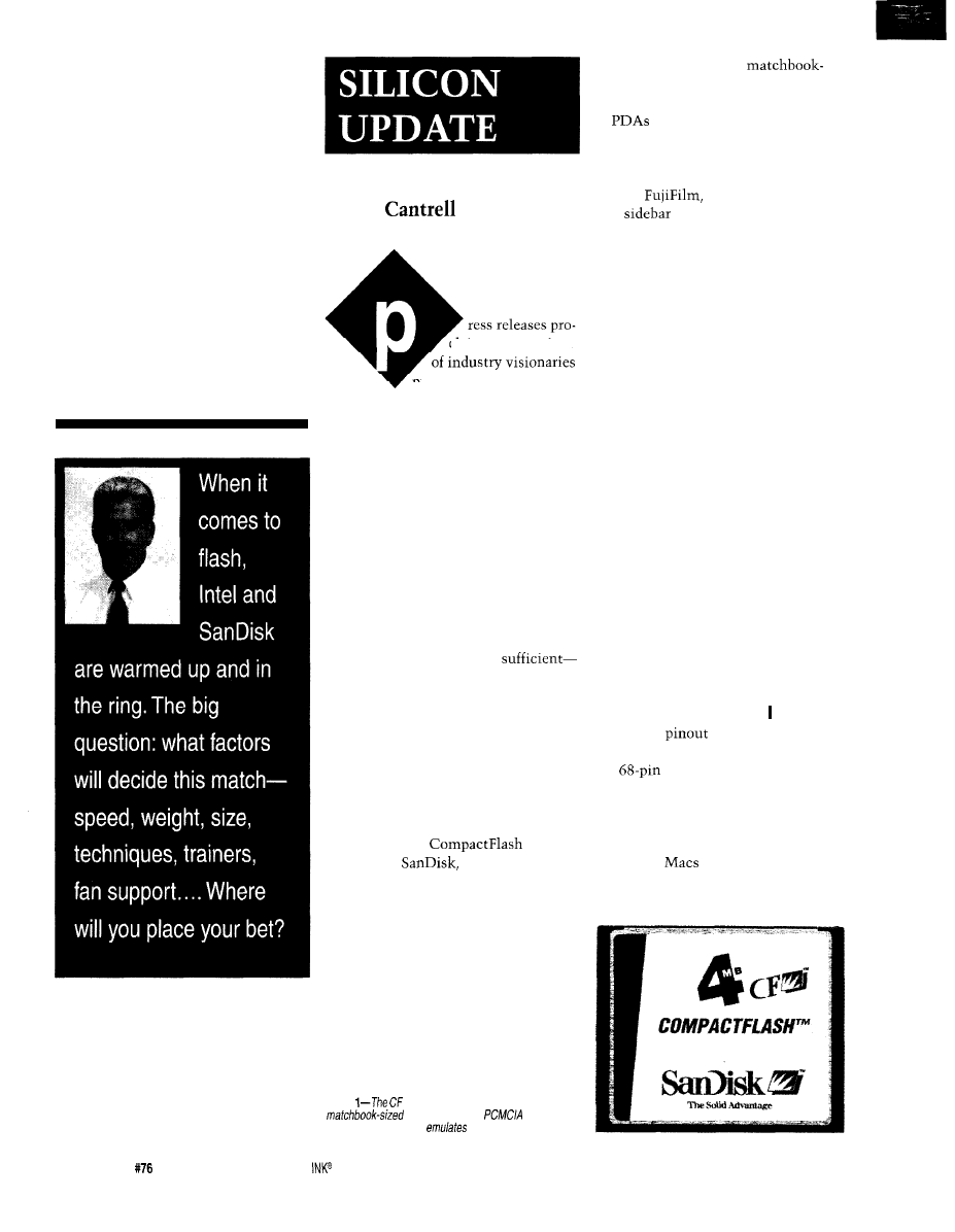
Flash Fight
Flares
Tom
claim a consortium
promising to deliver new
technology. The fax then shifts into
overdrive as retaliatory PR from an-
other hastily formed alliance touts a
similar, but incompatible, solution.
For Joe or Jane Blow, high-tech
widgeteer, it’s tempting to don a flak
jacket and duck down. But, that’s not
an option in a business where you’re
quick or you’re dead.
Of course, choosing wrong can be
career limiting as well. But, at least
you go down in flames rather than
being meekly led to slaughter.
Peruse each camp’s team. A com-
petitor is in group A, so join to keep an
eye on them. Oops, your biggest com-
petitor or favorite supplier belongs to
both
teams!
Technical evaluation of the alterna-
tives is necessary-but not
for choosing a winner. High tech has
lots of better mousetraps that failed for
marketing and business reasons.
And, here they go again. In one
corner, we have
(CF),
coached by
and in the other,
the Miniature Card (MC), backed by
Intel. Will it be a quick knockout or a
split decision?
HIGH STAKES
As shown in Photos 1 and 2, respec-
tively, the CF and MC are both tiny
cards that pack large amounts of flash
Photo
card packs megabytes of flash into a
package. Like ifs
predecessor, the card
an IDE disk drive.
(or other) memory into
sized packages.
Besides obvious applications such
as
and portable data loggers,
interest is fueled by the emergence of
digital cameras and digital film. That’s
why the teams include names like
Kodak,
Canon, and Polaroid
[see
“Team Rosters”).
In many ways-thankfully, not too
many-CF and MC can be considered
downsized PCMCIA cards. Indeed,
both offer PCMCIA adapter gizmos so
new cards can plug into existing slots.
It’s no secret I’ve been something of
a PCMCIA naysayer from way back.
What started as a simple memory card
suffered badly from creeping specitis.
The profusion of Types (I, II, and
III), some wild and crazy connector
schemes, and a dubious mishmash of
OS and driver software gave a new
meaning to plug-and-pray. Neverthe-
less, PCMCIA can claim some success,
especially in notebook PCs.
Presumably, the new standards
won’t suffer the same fate. That they
came up with names you can say gives
hope that the people in charge are on
top of things.
Sharing basic form factor, market
aspirations, and PCMCIA-retrofit path,
CF and MC are otherwise quite differ-
ent under the hood. Let’s take a look.
The CF
shown in Table
1
may look familiar since it’s similar to
the
PCMCIA predecessor. As
before, CF makes the flash look like an
IDE disk drive.
IDE DISK, THEREFORE SPIN?
The beauty of such a scheme is that
all PCs, and indeed most other plat-
forms like
and workstations,
already have software drivers built in
or easily available.
74
Issue
November 1996
Circuit Cellar
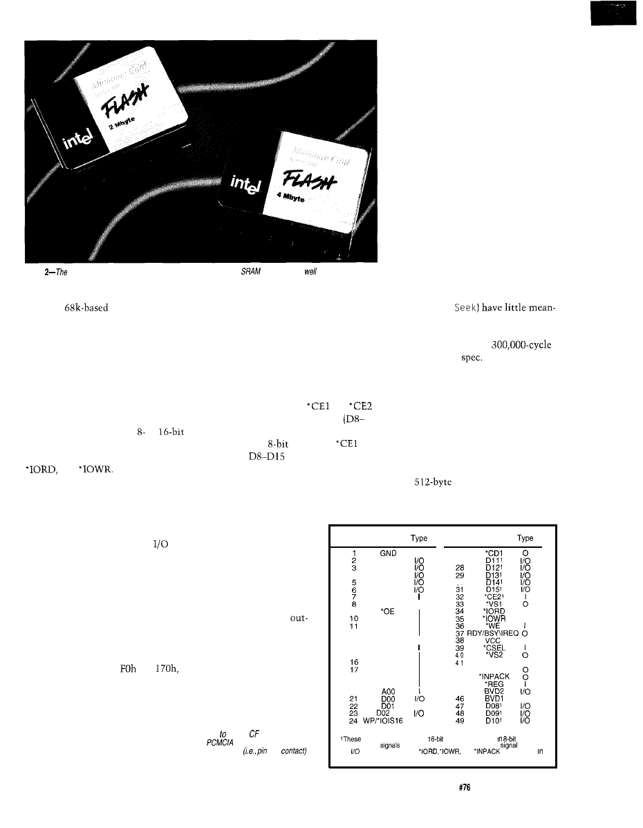
puts let the card request 5 V, 3.3 V, or
an even lower unspecified voltage.
The *REG pin is a kind of address
line that chooses between various
card-configuration and control regis-
ters and the IDE register map. The
former are normally accessed at card
insertion to determine card capabili-
ties and to configure it in the proper
mode. Subsequently, flash data trans-
fers rely on IDE registers (see Table 2).
For those who aren’t experts about
PC disk stuff-don’t worry, I’m not
either. It seems a rather simple matter
of setting up the sector (5 12 bytes)
address (head, cylinder, sector), issuing
a command, transferring the data, and
monitoring the status.
Photo
MC is effective/y a big memory chip that
accommodates
and DRAM as
as flash.
The command list includes all the
On the downside, the on-card con-
troller (a
custom chip from
Motorola) adds to the CF card’s cost.
The amount and relative importance
of the adder is a point of contention.
Though some may argue whether or
not making the flash look like a disk
drive is elegant, there’s no doubt that
adding intelligence on the card makes
life easier for the host.
Most activity centers on a couple
dozen pins, including the or
data bus, some address lines, and basic
control signals such as *OE, *WE,
and
Actually, the CF card can be config-
ured at *RESET in a number of modes,
such as primary, secondary, contigu-
ous, or memory-mapped I/O and so on.
There’s even a “True IDE” mode that
changes the function of a few
pins
to mimic the disk interface electrically
and in software.
Once you cut past the gobbledy-
gook, they’re simply different ways,
largely relics of past PC hacks, of rout-
ing commands and data into the card.
Primary and secondary modes place
the CF IDE surrogate registers at the
same I/O addresses traditionally allo-
cated to disk drives (1
and
respectively). However, to preserve
these I/O addresses for real disks, con-
tiguous-I/O mode lets registers be
mapped to other I/O addresses. All the
I/O modes rely on CPU In/Out in-
structions (i.e., using the IORD and
IOWR pins) for access.
By contrast, the memory-mapped
mode allocates the card to the PC
memory space, so access relies on the
*OE (read) and *WE (write) pins. In a
clever memory-window feature, refer-
ences to incrementing addresses are
funneled across the on-card FIFO. This
offers handy instructions like
REP
MOVSB
(byte)or
REP MOVSW
(word).
disk-related stuff for compatibility,
though many of the commands (e.g.,
R e c a l i b r a t e ,
ing for flash. Even the Wear Level
command needed for earlier flash cards
is ignored thanks to the
write-endurance
Ultimately,
almost all the action centers on the
basic
read
and
write sector.
Both modes rely on
and
to access low (DO-D7) and high
D15) bytes of the data bus, respec-
tively. For an
host, only
is
used, and
(and the host) con-
nect to DO-D7.
In the old days, flash technology
required a separate, higher-voltage
(e.g.,
12
V) power supply for writing.
But, that hassle went
away with the appear-
ance of single-voltage
flash chips.
Figure 1 shows the register setup for
read sector.
The card can be config-
ured for Logical Block Addressing,
which substitutes a simple linear
translation (i.e., Block O-n) for the
somewhat archaic head, cylinder, and
sector specifiers. Both ways point to a
single
block of flash.
Issuing the command causes the
card to go busy (status bit and pin), get
Number
Name
Number
Name
The bad news is, with
the quest for lower pow-
er, the voltage keeps
shrinking. The VS 1 and
VS2 (voltage sense)
DO3
DO4
4
DO5
DO6
DO7
‘CEI
A10
I
9
A09
A08
12
A07
13
v c c
14
A06
26
27
30
I
I
RESET I
42
*WAIT
43
44
45
I/O
50
GND
Table
l--Though
reduced from 68
pins 50, the shows its
roots in the electrical and
mechanical
and
interface.
1 5
A05
A04
A03
18
A02
19
A01
20
I/O
0
25
*CD2
0
signals are
needed
for
access and are not
systems.
Dual-purpose
show the the memory-only interface
before
the
interface signal. The
and
are not used
the memory-only Interface.
Circuit Cellar INK@
Issue
November 1996
75
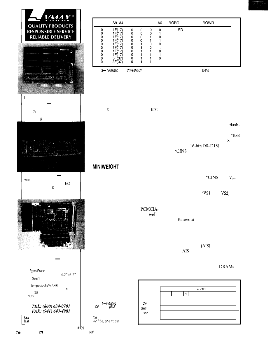
ENHANCED SOLID STATE
DRIVE
$110”
4M Total, Either Drive Bootable
Card 2 Disk Emulator
Flash System Software Included
FLASH
SRAM. Customs too
486 SLAVE PC CALL
up to 4 Boards to One Host PC
Fast Data Transfer and
PC-1 04 Port, IDE Floppy Control
ndependent Processors on One Bus
No Special Compilers Needed
TURBO XT
w/FLASH DISK
$188”
To 2 FLASH Drives, 1 M Total
DRAM to 2M
FLASH On-Board
CMOS Surface Mount,
2
Par, Watchdog Timer
Ail
products are
PC Bus Compatible. Made the
U.S.A.,
Day Money Back Guarantee
1, Qty breaks start at 5 pieces.
TEMPUSTECH, INC.
for
response!
295 Airport Road
Naples, FL 33942
‘REG
A3 A2 Al
= 0
= 0
Even
Data
Error Register
Sector Count
Sector Number
Cylinder Low
Cylinder High
Select Card/Head
Status
Alt Status
Drive Address
Even WR Data
Features
Sector Count
Sector Number
Cylinder Low
Cylinder High
Select Card/Head
Command
Device Control
Reserved
Table
a
disk
card presents an IDE-compatible register map host
the sector from flash into the on-card
The MC is thus like a big memory
FIFO, clear busy, and signal (status bit
chip.
and interrupt) data availability. The
While most of the action centers
host can read
512 bytes or 256
words
around flash, the direct access (via
of data from the FIFO.
For writes, notice w/o Erase. A
w
r i t e
e c t o r erases the
data
which wastes a lot of time. Instead,
use erase sector and then write
without erasing at high speed.
The CF on-card micro handles ECC,
bad-block mapping, dynamic adjust-
ment of performance versus power
consumption, extensive self-testing
and diagnostics, and the gory details of
accessing the flash.
CONTENDER
The main visible difference for the
MC is its elastomeric connector, which
is best described as a conductive rub-
ber ribbon cable squished between the
card and socket.
Not surprisingly, there are plenty of
connector claims on both sides. The
CF corner rejoins that the
like pin and socket they use is
proven, and in fact, specs up to 10,000
insertions versus only 5000 for the MC.
The counterpunch is that the elas-
tomeric connector is easy to replace
and use. It tolerates real-world abuse.
To me, the connection-not con-
nector-differences are much more
profound. As shown in Table 3, the
MC carries a full (AO-A24) address
bus. Not a big deal, except that it indi-
cates there’s no on-card intelligence.
l
CE, *OE, *WE, etc.) of the MC makes
it amenable to other technologies like
ROM, SRAM, and even DRAM. (No-
tice the l RAS and l CAS signals.)
There’s a little more to explain. The
*BUSY line handles the timing of
memory writes, but it can simply be
grounded for a full-speed memory.
is an input to the card selecting
(DO-D7) or
operation.
(card insert) is a grounded
output on the front of the card that
makes contact before the rest of the
interface. *CD (card detect) is also a
grounded output but grouped with the
other signals. Thus,
(plus
and GND) give the host early warning
of the card’s arrival.
Similar to CF,
and
two
voltage-sense outputs, request differ-
ent voltages (e.g., 5 V, 3.3 V, and a
future lower one). The MC also adds
keying of the card and socket to pre-
vent
(see Figure 2).
Otherwise, the only difference from
a memory chip is that the MC includes
an information block at the beginning
for what’s called the Attribute Infor-
mation Structure
(see Table 4).
The
characterizes timing de-
tails and power requirements for up to
four blocks of on-card memory. More
information is provided for
and memory with burst capability.
Issue
November 1996
Circuit Cellar
Figure
access to
a
sector
bytes) simply
requires specifying the address
and sector count and issuing
command such as read,
Bit-> 7 6 5 4 3 2 1 0
Comand (7)
20H
C/D/H (6) 1 LBA
Drive
Head (LBA 27-24)
Cyl High (5)
Cylinder High (LBA 23-16)
Low (4)
Cylinder Low (LBA 15-8)
Num
(3)
Sector Number (LBA 7-O)
Cnt (2)
Sector Count
Feature (1)
X
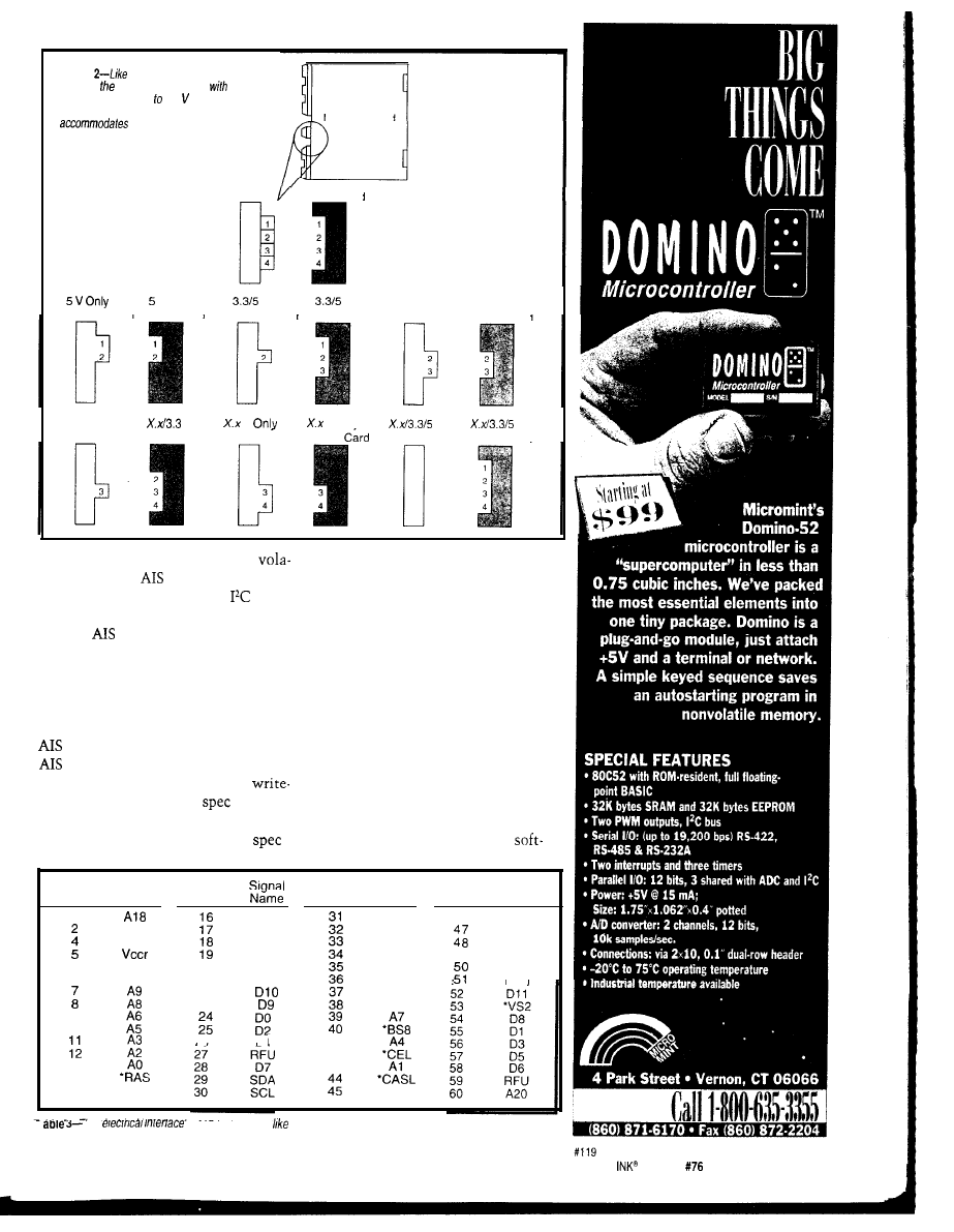
Figure
many of
today’s
designs, MC is forced to deal
the migration from 5 3.3 and
beyond.
A
mechanical keying scheme
the
myriad of
combinations.
Miniature Card
Host
Miniature Card
Host
V Only
Miniature Card
v
Host
v
3.3 v Only
3.3 V Only
Miniature Card
Host
Miniature Card
x.x/3.3 v
v
V
V Onlv
v
v
Host
Miniature Card
Host
Miniature
Host
Miniature Card
Since DRAM cards are usually
also says the host should detect the
tile, storing the
is a problem. To
protect status, without saying how.
solve it, the MC relies on the
inter-
face (using the SDA and SCL pins) to
SOFT TOUCH
read the
from a serial (EEP)ROM.
Simplifying the card by removing
A mechanical key prevents DRAM
cards from plugging into sockets that
can’t handle them.
Hosts that can handle all types,
including DRAM, first try to read the
serially. If that doesn’t work (i.e.,
checksum fails), try a parallel read.
The card provides an optional
protect switch which the
implies
should physically prevent writing (e.g.,
the controller means host software does
the housekeeping. Proponents argue
that today’s PCs have enough power to
spare a controller’s worth of CPU cy-
cles in return for lower-price cards.
Rather than using a controller to
fool the PC into thinking an MC is a
disk, a layer of software known as a
Flash Translation Layer (FTL) is sand-
wiched between the OS and hardware.
gate
the WE’ line). However, the
This driver and BIOS extension
Pad
Signal
Number
Name
1
A l 6
A l 4
‘CEH
6
A l l
9
10
13
14
15
A24
Pad
Number
A23
A22
‘OE
D15
2 0
D13
21
D12
22’
2 3
2 6
D4
Pad
Signal
Number
Name
A19
A l 7
A l 5
A l 3
A l 2
*RESET
A10
l
vs1
41
42
43
*CASH
Pad
Signal
Number
Name
46
‘ C D
A21
‘ B U S Y
49
‘ W F
D14
RFU
I
I
ne
for MC‘ looks more
a memory chip than a disk drive
Circuit Cellar
Issue
November 1996
7 7
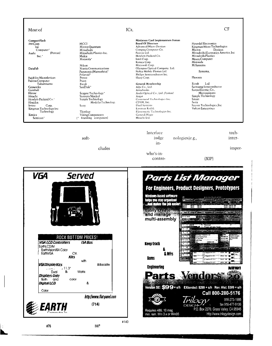
Team Rosters
the big
names in electronic systems including
PCs, and digital cameras are choosing between the
and
MC
standards, with many hedging their bets by supporting both.
Ass”.
AMP
Apple
Optical Co
Canon
Carry Computer Eng.
Centennial Technologies
Cirrus Logic
Systems Inc.
Eastman Kodak Co.’
Epson’
Technology
L t d .
Fujitsu
America
co.
Electric Inc.
Sensors
Kingston
Corp.
LG
Devices
N E C ’
Sanyo
SMART
T D K
Inc.
Quantum
Inc.
Consultants Inc.
Nikon Corp.
NRC
Inc.
PC Card Packaging
Technologies
I’NY Electronics
co.,
Ltd.
SCM
Modular
Corp.
ware is what turns a disk command
They hope to standardize the FTL
vcrsy revolves around the vagaries of
into the low-level flash cycles.
and form a Common Flash
flash. MC cards based on other
The downside of this and any
specification. It’s premature to
ROM and RAM)
ware-driven scheme is the dreaded
the outcome, but the MC roster
face like any other memory chip.
“driver disk” dilemma. Anytime host
the necessary players.
Indeed, a subtle but possibly
and/or memory technology changes,
Remember, most of the
tant advantage for MC is the so-called
it’s time to fumble for the right floppy.
charge (i.e., controller or host)
Execute-In-Place
capability. This
LCD’s
Here
far PC
Monochrome LCD Contrdler
$160
LCD Controller
$280
Analog Input
(VGA to LCD!]
$599
I NEW! Touch Screen
Analog resistive touch screen
controller $249
Include LCD. Controller,
7.4” 9 4” 10.4”
Starting at $220
Mono.
Scan Active
in Stock
new
surplus
displays from
$99
Monitors
Desktop LCD ISA Controller
Monochrome Monitors
Starting at $400
Monitors
Starting at $600
See Earth on the Worldwide Web!
Ph.
448-9368
Fax: (714) 448-9316
Computer Technologies
78
Issue
November 1996
Circuit Cellar
parts lists for
products in
development
. ..And after!
Of:
l
Part
Specs Dwgs
l
Suppliers
l
and Kit Lists
l
Product Costs
l
Stock
Address
Section
Description
OOH-OFH
PC Card Compatibility Area
Reserved
for
PC
Card
identification Data
Card Type
Identification Data
Data
Compatibility Data (1)
Memory Technology
Burst Data (1)
DRAM Data (1)
Reserved for future use
Compatibility Data (2)
Memory Technology
Burst Data (2)
DRAM Data (2)
BOH-BFH
Reserved for future use
COH-CFH
Compatibility Data (3)
Memory Technology
DOH-DFH
Reserved for future use
EOH-EFH
Compatibility Data (4)
Memory Technology
FOH-FFH
Reserved for future use
feature means code can run in the card
without being loaded into RAM.
SPLIT DECISION?
Today,
CF is ahead in actual
ins and production, but MC is
shalling a formidable response.
I like things about both cards. In
particular, the smaller form factor
(25%
the size of PCMCIA) enables
truly portable gear. Size limits dis-
courage temptation to bloat the
The controller fight seems exces-
sive given the PC- and PCMCIA-cen-
tric presumptions that fuel it. For
instance, how many desktop PCs have
PCMCIA slots? There’s plenty of PC
software (OS, FTL, CFI, etc.), but what
if you’re making a card-playing gadget
using a low-cost embedded micro?
Although list prices are high (-$50
per MB) and densities are just entering
the double-digit range, no doubt the
price will go down and density up. The
cards may first appear in bleeding-edge
products like digital cameras, but
eventually they’ll be everywhere.
Two standards may be best since it
gives some choices and encourages
competitive pricing. I’d rather deal
with two simple, stable standards than
one complicated, slippery one.
It doesn’t look like a quick knock-
out, so your best bet is with the card
you like. If your application is prima-
rily flash-oriented and benefits from
the transparency of a built-in disk-like
interface, go with CF. If
expect to
use
memory technologies and
need XIP, bet on an MC.
q
been working on
chip, board, and systems design and
marketing in Silicon
for more
ten years. Hc may reached by
Table 4--Each MC
has an
area of memory called the
Attribute information Structure
defines the type,
amount, and operating
characteristics of the memory
on the card.
E-mail at
telephone (510)
or by
(510)
Assn.
Box 51537
Palo Alto, CA 94303
(415)
Fax: (4151 493-1871
Corp.
140 Caspian Ct.
Sunnyvale, CA 94089
(408) 542-0500
Fax: (408) 542-0503
Intel Literature Packet
Intel Corp. Literature Center
P.O. Box 7641
Mt. Prospect, IL 60056
(916) 356-7368
Fax: (847) 296-3699
Miniature Card
Intel Corp.
5000 W. Chandler Blvd.
Chandler, AZ
(602) 554-8080
Fax: (602) 554-7436
Forum
1900 Prarie City Rd.,
Folsom, CA 95630
(916) 356-7060
Fax: (916) 356-8607
MinatureCardQccm.fm.intel.com
425
Very Useful
426 Moderately Useful
427 Not Useful
Circuit Cellar INK@
Issue
November 1996
7 9

The Circuit Cellar BBS
bps
24
days a week
(860)
incoming lines
Internet E-mail:
seems a week doesn’t go by without my receiving a message from
someone asking if they can get to the public message areas or the
file areas of the BBS via the Internet. Right now, the answer is
no. However, we’re working on a solution.
divulge more details in the coming months, but in an effort to
reduce some of my f-mail load, wanted to let you know that such
access really is on ifs way. Just be patient for a little while longer.
Thanks.
The following message threads may be obtained in their entirety
either from the BBS or on disk. See “Article Software” at the end of
this column for more information.
Blinking neon lamps
I’ve wanted to use this thread for several months now,
but have never had the room. It starts with a simple enough
question: how do you make a circuit that flickers a neon
lamp so it looks something like a candle burning?
That simple question touches off an extensive discussion
of techniques, theory, and proposals that is almost amusing
in its intensity at times. Definitely a fun diversion.
How to burn a GAL
For years, we at Circuit Cellar have received pleas from
people to present a PAL programmer project. We’ve done
EPROM programmers, so a PAL programmer can’t be
that
hard, can
Well, when the basic device programming information
just isn’t available like it is for EPROMs, such a project
takes on orders of magnitude more difficulty. Different
chips require different programming algorithms, and manu-
facturers refuse to release detailed information.
This next thread starts with just such a discussion.
You’d think that by bringing it up in a forum frequented by
hundreds of engineers from around the world, someone
might have some insight. Such wasn’t the case.
Different people posit different theories as to why the
manufacturers refuse to divulge details, and one overseas
caller even posts a partial programming description in Ger-
man, but nobody has the definitive answer. It makes for
some interesting reading.
Metal detectors
In this age of AIDS and concern over blood- and
borne diseases, hospitals can’t be too careful in protecting
its staff from accidental cuts and sticks. This thread starts
with a question of how to scan a laundry bag for metal ob-
jects. The concern is that needles and other sharps objects
that accidentally get into soiled linen bags at a hospital
could injure workers handling the bags.
The only catch is the bags are loaded on metal carts with
metal walls on three sides. Is there a way to scan for metal
in the bags by simply passing the carts through some de-
vice?
Some interesting ideas are brought up, including the use
of all-plastic carts, passing the bags through a metal detec-
tor after being unloaded but before being dumped out, and
using the hospital’s MRI equipment (it was a joke).
All the suggestions have one problem or another, and the
issue isn’t completely resolved. Do you have an idea? Take
a look to see if it was already brought up.
Parallel Port Key
In the ultimate example of thread drift, this discussion
starts with a question about parallel port dongles, and ends
up talking about the use of different AC voltages and fre-
quencies used in various countries and their affect on equip-
ment.
How does such a transition take place? After some initial
talk about the theory behind the need for dongles and how
they work, someone suggests that they use a short cable to
move the dongles away from the back of the PC to reduce
the amount of clearance necessary behind the computer.
Another user points out that the cable length is limited
by the port drivers used in the PC. He retorts with, “Okay,
so you add some power
switching rectified and filtered
220 VDC from the mains. No problem with juice then,
right?” It doesn’t take long for someone to point out that
220 V isn’t used in some countries and the entire discussion
takes an abrupt turn to the new topic.
If you’ve wondered what voltages are used in other coun-
tries and why, this is a neat thread. Some of the input from
our overseas callers is quite valuable.
Circuit Cellar
Issue
November 1996
81
Telephony design
3306
From: Lyndon Walker To: Jesus Lares
3284
From: Jesus Lares To: All Users
I think I read somewhere in this BBS that if I wanted to
design a telephony product (e.g., Caller ID box, small PBX,
etc.) for commercial purposes (sell in small quantities), I
could use
with Part 68 registration like Xecom’s or
Cermetek’s.
Yes and no. If you use a DAA with user-transferable
registration, then you don’t need *Part 68 certification.
However you may very well need Part 15 certification which
is a whole other ball of wax.
Msg#: 3312
From: Jesus Lares To: Lyndon Walker
Can I slap together a controller, a DAA, and some soft-
ware, and then sell the product without having to go through
FCC certification or approval?
Msg#: 3288
From: Jeff Bachiochi To: Jesus Lares
Yup! You take on the
certification. However, if
your circuitry has any kind of oscillator over 100
the
system is considered a transmitter and must pass interfer-
ence testing. They get you coming and going. Of course, the
FCC is there to protect us from ourselves.
Thanks for your reply. I do not know if you are familiar
with FCC certification procedures, but I will ask you the
following question anyway. Is Part 15 certification within a
small budget range (hundreds) or is it out of the question
(thousands)? I ask you this because, I used to work for a
company that developed a call controller, and they paid
around $10,000 for certification (both Part 68 and 15).
3369
From: Lyndon Walker To: Jesus Lares
3290
Most of the money will be for the testing lab you send
your device to. Part 15 certification fees are less than $1000
and Part 68 is $180. These are fees paid to the FCC.
From: Jesus Lares To: Jeff Bachiochi
Thanks for your reply. If I understand you correctly, I can
use a
crystal and a micro, and I’ll be home free.
Right?
As far as the cost of having the device tested, I’ve never
done it myself. But from memory of when we looked into it
a few years ago, the price was around $5000 assuming all
went well the first time around.
Msg#: 3337
3355
From: Jeff Bachiochi To: Jesus Lares
From: George Novacek To: Jesus Lares
Last time I looked, that was the case. They don’t seem to
leave many loopholes like that. Good luck!
3307
From: Lyndon Walker To: Jeff Bachiochi
It depends. The certification itself is not that expensive.
It will be in the hundreds. But you must submit a test re-
port with your application. And that is when it is going to
cost you in thousands to tens of thousands, unless you have
the equipment to do it yourself.
Shouldn’t that be 9
3338
From: Jeff Bachiochi To: Lyndon Walker
Do you know something I don’t? We’re not talking audio
as in tones, but oscillator as in micro.
You also must be qualified. At one point, just a regis-
tered professional engineer was good enough. At some point,
I am given to understand (I have not dealt with FCC for 7
years), the engineer needed to get on the list approved by
FCC.
Msg#: 3370
Last, if you go to an independent lab and things go wrong,
watch out! At roughly
it is very easy to rack up a
huge bill for retesting or in-lab development.
From: Lyndon Walker To: Jeff Bachiochi
Quoting from 1996 Compliance Reference Guide: “The
spectrum shall be investigated from the lowest radio-fre-
quency signal generated in the device, not below 9
up
to at least the 10th harmonic of the highest fundamental
frequency or 40
whichever is lower.”
CE approval
This is from Part
certification section of Compliance
Engineering’s reference book. The actual section it’s taken
from is not mentioned, but the
figure appears a num-
ber of times, so I don’t think it’s a typo.
From: Brian Farmer To: All Users
We are a manufacturer of light industrial equipment
used in Europe. We would like to gather information regard-
ing the most cost-effective way to obtain CE approval. At
82
Issue
November 1996
Circuit Cellar
this point, we believe there will need to be some modifica-
tions to our equipment. Anyone with experience in this
area, please respond. Thank you.
From: Pellervo Kaskinen To: Brian Farmer
Based on our experiences, there may not be a truly
effective” way..
The problem is the general unavailability
in this country of the basic standards. I mean..
are
available, but not in the public libraries and similar
charge form. I think we spent about $7,000 for our set. We
started with just a couple of the documents, by recommen-
dation of our European office. That gave references to fur-
ther documents that we believed would be relevant.
We tried to be very selective, but after getting the next
set, we found further references that required additional
purchases. Luckily, after the third round we were pretty
well stocked with what we needed.
There is a certain amount of information in Compliance
Engineering
Magazine. It is free for qualified persons. In
fact, it contains ads for the testing labs, the instrument
makers, and for the bodies capable of providing you with
the European standards. Looks like one of the more aggres-
sive document outlets nowadays is the Danish Testing
Authority (whatever its actual name.. They sell the
documents in English versions, despite their na-
tionality.
If you are using UL for anything, your best bet might still
be using them-they are building up their EU connections.
I’m sorry, but I cannot give a comprehensive answer,
because the relevant rules vary by the type and by the in-
tended market of your product. I would say, though, that
you have to meet the Low-Voltage Directive in any case.
Noise rules vary, but most small appliances and similar
products already have to meet the power factor and har-
monic content rulings in addition to conducted and radiated
noise limits. The scope of the harmonics and power factor
rulings is going to be expanded in June 1998 to cover virtu-
ally all items using AC power. Presently, below some 80 W
and above 16 A (at 230 V) are outside of the scope.
Besides the limits on emitted noise, there are require-
ments for noise immunity. The rules on that front generally
do not require complete absence of any malfunctioning, but
instead that the failures do not cause danger. Your product
O E S Y O U R
B
I G
- C
O M P A N Y
MARKETING DEPARTMENT COME
MORE IDEAS THAN THE
ENGINEERING DEPARTMENT CAN
C O P E
W
I T H
? A
R E Y O U A
S
M A L L
COMPANY THAT CAN’T AFFORD
FULL-TIME ENGINEERING STAFF
ONCE-IN-A-WHILE DESIGNS?
T E V E
A N D T H E
D
E S I G N
W
O R K S S T A F F M A Y
SOLUTION.
HAVE A TEAM OF
ACCOMPLISHED PROGRAMMERS
AND ENGINEERS READY TO
PRODUCTS OR SOLVE TRICKY
ENGINEERING PROBLEMS.
HETHER YOU NEED AN
ON-LINE SOLUTION FOR A
PROBLEM, A PRODUCT FOR A
STARTUP VENTURE, OR JUST
EXPERIENCED CONSULTING, THE
D
E S I G N
W
O R K S I S
WORK WITH YOU.
UST FAX ME YOUR PROBLEM
WE’LL BE IN TOUCH.
RIGEL
Corporation introduces
its newest line of boards,
the
Our 8 and
boards
are designed for immediate placement into a
Controller Area Network.
The
features the Siemens SAB
processor, and includes an RS232 serial port, 1 I/O bits,
five
timers,
system clock, built-in CAN
interface, 4 channels of PWM,
1 MB of FLASH memory
and
of SRAM.
THE RIGEL DIFFERENCE
Assembly,
and Forth.
FOR MORE INFORMATION VISIT OUR
WEB SITE
or contact us at
RIGEL Corporation,
PO BOX 90040, GAINESVILLE,
FL 32607
Telephone
373-4629
373-1786
42
Circuit
Cellar
issue
November 1996
83
must tolerate certain power-line transients and transients
coupled to any and all data lines and similar that are longer
than about 6 ft. The length requirement is implicit because
the noise is injected to the cable by a I-meter trough,
through which your cable is run. Cables that are too short
for the coupling device are excused.
Being excused does not mean they do not have to meet
some noise-immunity tests. The static-discharge test is to
be applied to the peripheral devices as well as to the main
console (in our case).
A big hassle is the labeling and the instruction area. The
basic idea is that you either have to provide native language
warnings in whatever country your product is sold, or use
graphical symbols and explain them in the manual at the
native language.
First, the symbols have to be chosen from a set of
defined (IEC or
sets or they have to be designed to
meet rather stringent guidelines regarding their absolute
and relative sizes and other details. I think some of the
documents you should consult are IEC 447 and IS0 7000.
Oh, one last thing you absolutely have to cover is the
test-voltage levels. It is a bit complicated because you have
to define the use types and “pollution” categories (water
and dust effects). And this leads to direct and
surface distance requirements of all line-side traces that
generally exceed what the American designers have grown
accustomed to.
The transformer primary-to-secondary insulation test
here is typically 1,500 V, but a rough estimate is that the
European rules are going to be satisfied only with a
l-minute test. Or even higher, if the pollution
level appears to require tightening of the rules.
A related requirement is that the yellow/green protective
ground lead be able to carry enough current (25-A test min.).
And it has to be terminated in a properly marked (PE = Pro-
tective Earth) stud that is not used for any other purpose.
I hope this gives you a starting point. If you have more
specific questions, I’ll try to help, but be aware that the
“devil is in the details.” What looks like a completely plau-
sible set of rules can be totally invalidated by a minor over-
looked condition of intended use and so on.
Current limiters
7139
From: Mark Delaune To: All Users
I am looking for a
current limiter. I was think-
ing about using a differential op-amp sensing current through
a resistor and taking the output of this into a comparator
with lots of hysteresis to shut the supply down.. .or perhaps
to
fire an SCR once the comparator switches, making the
user recycle power. Any ideas!
From: Pellervo Kaskinen To: Mark Delaune
What kind of power supply are you talking about? The
limiting is common on linear power supplies,
while switchers typically shut completely off. After a few
milliseconds they try a new (possibly soft) start.
In fact, the SCR is usually paired with a fuse and only
intended for cases where the pass transistor is shorted and
would let the whole supply voltage reach the 5-V circuit.
Then, it is better to short the supply, blow the fuse, and
Firing an SCR to short circuit the output of a power
protect the rest of the circuits.
supply is a last resort as far as I’m concerned. You tend to
get more than you bargained for. The SCR does not short
the output completely; there is likely to be a volt or two
remaining. If the power supply has a 5-V,
15-A
capacity,
your SCR has to dissipate
30 W. A big heat sink.
If you suspect a load-side short circuit or overload, then
the current limiting with
characteristics is an
attractive choice. Minimize the overall power dissipation,
especially on the pass transistor.
The one most important side effect from the
characteristics is that often the loads require quite a bit of
inrush current when turning on. A
limiting by its
very nature provides a reduced current at this situation and
may prevent the load from starting altogether. I had such an
experience a long time ago and have since favored straight
current limiting without the foldback.
Sources for optical interface circuits
3878
From: Mike Aulik To: All Users
I’m hopeful someone can point me in a direction.
I am on a contract project for a medical school. I need
names of companies that make
and/or interface hard-
ware that will allow a beam of light over a fiber-optic cable
to act as a switch. Sources for the cable and any related
components would be greatly appreciated. Also, if anyone
can suggest sources for design information in this area, I
would greatly appreciate that as well. Thanks much.
Msg#: 3976
From: Pellervo Kaskinen To: Mike Aulik
Simple answer: Microswitch division of Honeywell.
I believe there are several more, like Banner, but truly
the first name that comes to my mind is Microswitch.
84
Issue
November 1996
Circuit Cellar
Moreover, they are quite well represented all over the coun-
try. You can go to an electrical contractor supply house and
it’s likely that they will have at least the necessary catalogs.
Or you can go to any one of the myriad electronics distribu-
tors. They’ll have Microswitch among their sources.
3882
From: Lyndon Walker To: Mike Aulik
What kind of switch? What distance are you running?
How fast do you need to switch!
For relatively slow (to a few 100
optical communi-
cation over short distances,
plastic fiber works
well and is easy to use. Look at the AMP Optimate DNP
connectors. They also make plastic fiber. I think Digi-Key
still carries them.
Siemens makes optical connectors with integrated detec-
tors and emitters. Motorola used to have a similar system,
but they just made it obsoleted.
Plastic fiber is especially attractive because it doesn’t
require special tools and is very inexpensive. I was paying
about
per meter in small quantities three years ago.
If you just need, say, a low-side power switch controlled
from fiber-optics, two transistors, a few resistors, and the
Motorola FLCS (can still be purchased if you just need one
or two systems] optics are all you need. Cost less than
$10
total. For ultra cheap, just drill holes into
and photo-
detectors to make your own optical connectors. AMP
mate takes a bit more work, but it’s still pretty easy to use.
For the more sophisticated, faster “real fiber” stuff, look
at HP, Siemens, and Honeywell.
As far as design info, the Motorola Optoelectronics books
from ‘93 had sample circuits. A distributor may still have a
few of these older books. AMP has a good intro, A Techni-
cian’s Guide to Fiber Optics.
Digi-Key carries it (or used to).
It’s a basic intro to fiber, not a design manual.
We invite you to call the Circuit Cellar BBS and exchange
messages and files with other Circuit Cellar readers. It is
available 24 hours a day and may be reached at (860)
1988. Set your modem for 8 data bits, stop bit, no parity,
and 300, 1200, 2400, 9600, or
bps.
Software for the articles in this and past issues of
Circuit Cellar INK
may be downloaded from the
Circuit Cellar BBS free of charge. It is also available on
the Internet at
For those
with just E-mail access, send a message to
to find out how to request files through
E-mail.
Message threads summarized at the beginning of the
column are also available on the BBS for at least six months
after they are first posted. The subject line at the start of
each summary matches the subject used on the messages
themselves. Simply call the BBS and search for those
subject lines to find the message threads.
For those unable to download files or messages, the
software and messages are also available on disk. Software
for issues prior to 1995 comes on a
IBM PC-format
disk, one issue per disk. For issues from 1995 on, software
comes on a
PC-format disk, with three issues per
disk. Disks cost just $12 each. To order Software on Disk,
send check or money order to: Circuit Cellar INK, Software
On Disk, P.O. Box 772, Vernon, CT 06066, or use your Visa
or Mastercard and call (860) 8752199. Be sure to specify
the issue numbers with your order. Please add $3 for
shipping outside the U.S.
428
Useful
429 Moderately Useful
430 Not Useful
Whoever heard of a computer, “Yes it has ram, quit
rupting” for the
low price of “no it’s not a
Now where was I? oh yeah”, for the unbelievable
price of
These computers are AT&T
and were pulled from service, and now we have them.
pletely tested and guaranteed. They come complete with
case, power supply,
Intel
mother board, 2-drive bays,
dise VGA controller, 256k video ram, floppy and IDE hard
drive controller, keyboard controller, Intel bios, 4
sion slots (3-16 bit, l-8 bit),
ports, l-parallel port,
mouse port, 8 standard 30 pin simm sockets, and a
that s a long
4-meg of ram (standard I-meg 30 pin
I
hard drive and 3.5” 1.44 floppy
Offer
plus offer
plus offer
(Approximate shipping weight of offer
or offer #4-37 Ibs.)
The above should make an excellent diskless workstation,
a second computer, or a great start-up computer for a
ster.
Circuit Cellar INK@
Issue
November 1996
85
INTERRUPT
Bits and Bytes
w
e all have aversions to certain things in life. As get old and crotchety, worry less about apologizing for
what don’t like and considerably more inclined to seek out exactly what I do like. If Bob Pease (see last
month’s editorial) can count dead cars, guess can complain about how much I hate grass maintenance and
airline travel.
What do they have to do with computer applications? Nothing, I suppose. Going to the Embedded Systems Conference in San
Jose reminded me how much I hate crowded airports. And, while I was on the subject, I just thought I’d throw in the fact that lawns
aren’t my thing either.
Realize, of course, I’m just speaking for myself. love driving through Litchfield, CT where all the homes have baseball-park-sized,
scissor-manicured lawns. I’m just glad all that grass is theirs, not mine. However, anyone analyzing the effort that I go through in
maintaining a
groundcover would laugh themselves silly. save that story for another time.
While I perpetuate the nonexistence of my grass, it’s invariably my publisher, Dan Rodrigues, who makes commitments that cause
me to end up on planes heading west. Needless to say, this leads to getting even.
There’s nothing more fun than tormenting a publisher. When returned from the conference, I saw the perfect opportunity. Half
hunching over Dan’s desk, I remarked with a pained expression, “Dan, I’ve got some good news and some bad news about the
Embedded Systems Conference!”
He looked up from his spreadsheet. From experience, he knew that hearing bad news first wasn’t going to be music to his
accountant ears. Out of fiscal necessity, however, perhaps he’d better deal with it. He responded soulfully, “OK, what’s the bad news?”
Conjuring up my most disgusted and exasperated expression, I said in a defeated tone, “We only sold three magazine subscrip-
tions at the show!”
Just like the old joke about the engineer who offers to fix a broken guillotine (guess who’s next), you can always count on a
publisher with an accounting background to instantly react to such news by grabbing his chest and gasping for air. Twelve grand in
expenses divided by three subscriptions! Arrrghh!
But, Dan’s getting smart enough by now that he knows when I’m trying to scramble his abacus. He banged his hand on the desk
and stated emphatically, “Wait a minute! You weren’t supposed to be selling any subscriptions! Everybody in that place is already an
reader!”
“Almost gotcha,” I smiled. “Financial guys are so easy.”
As he was muttering something about “dumb engineers,” I couldn’t help but beam at the reality of
success and our
experience at the show. The only reason for the three subscriptions was that they came from foreign travellers who were worried that
they might miss an issue if the subscriptions weren’t placed eye-to-eye. More than half the exhibitors were advertisers, and virtually all
the attendees were readers. There wasn’t a booth I entered where they didn’t know
welcome us.
Although I might protest for weeks before getting on a plane to a convention, these days without exception I come back knowing
that what I’ve been doing all these years personally and with
hasn’t gone unnoticed. More and more people have made me aware
that the course we’re on and the knowledge we consistently present has positively affected their professional lives.
The only slightly pessimistic comment came from an industry maven who suggested that my decidedly conservative nature may in
fact be holding
from realizing its real (i.e., financial) potential. I reminded him that, in my experience, magazines that had
responded solely to stockholder demands are lucky if they’re a mere bit of their former BYTE. Call me conservative if you must, but
we still have our hands on all eight.
96 Issue November 1996 Circuit Cellar
Wyszukiwarka
Podobne podstrony:
circuit cellar1993 11
circuit cellar1994 11
circuit cellar1997 11
circuit cellar2004 11
circuit cellar2000 11
circuit cellar1995 11
circuit cellar2002 11
circuit cellar2001 11
circuit cellar2003 11
circuit cellar1993 11
circuit cellar1995 11
circuit cellar1996 11
circuit cellar2003 11
circuit cellar1997 11
circuit cellar1993 11
więcej podobnych podstron