1
Podstawy techniki
mikroprocesorowej
ETEW006
Przetworniki A/C i C/A
Andrzej Stępień
Katedra Metrologii Elektronicznej i Fotonicznej
Przetworniki A/C
metoda przetwarzania analogowo-cyfrowego
rozdzielczo
ść
i dokładno
ść
przetwarzania
czas próbkowania i przetwarzania mierzonego sygnału
parametry wej
ś
ciowe: pojemno
ść
i rezystancja wej
ś
ciowa przetwornika
rezystancja analogowych przeł
ą
czników determinuj
ą
ca rezystancj
ę
ź
ródła
mierzonego napi
ę
cia
automatyzacja pomiarów, mo
ż
liwo
ść
wykonania pojedynczego, wielokrotnego
pomiaru, z automatem programuj
ą
cym numery kanałów wej
ś
ciowych i
krotno
ść
powtarzanych pomiarów
sposób zapisu wyników przetwarzania, zwłaszcza dla przetworników o
rozdzielczo
ś
ci wi
ę
kszej od długo
ś
ci słowa maszynowego
wewn
ę
trzna konstrukcja i wewn
ę
trzne układy wpływaj
ą
ce na dokładno
ść
przetwarzania
jako
ść
poł
ą
cze
ń
na płytce drukowanej, sposób zasilania cz
ęś
ci analogowej i
cyfrowej
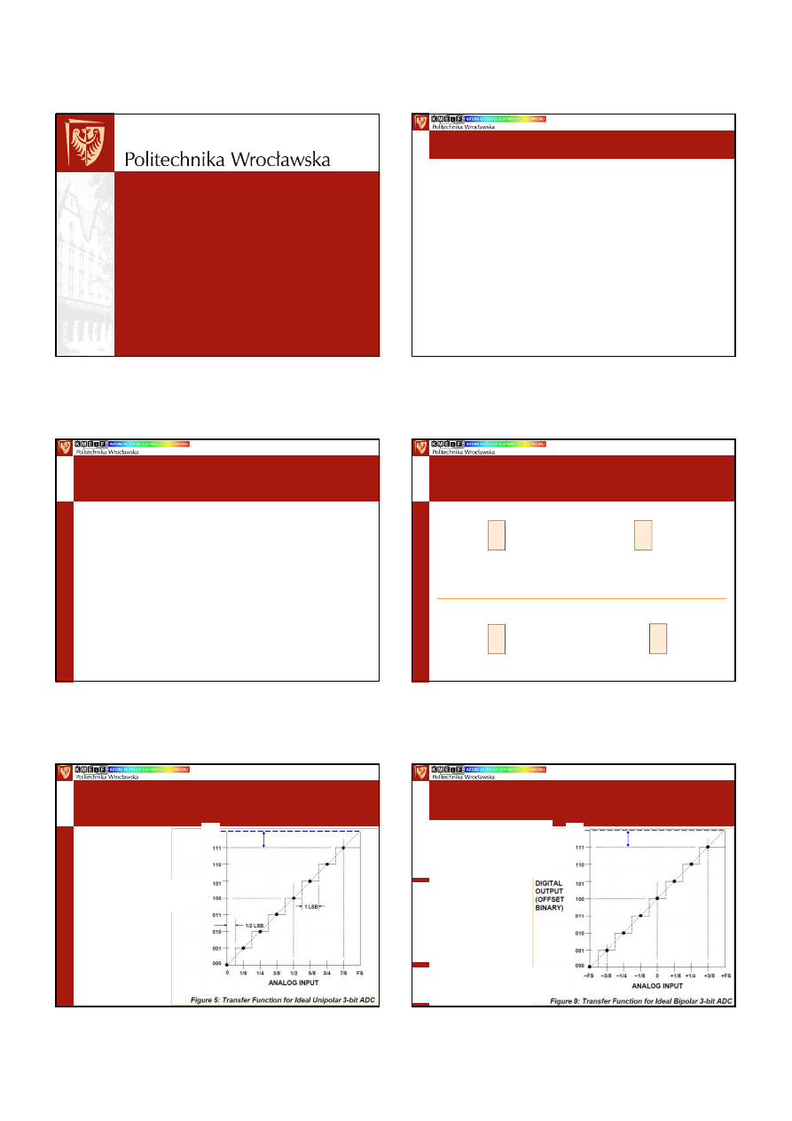
Rozdzielczość przetworników
poj
ę
cie ’pełna skala’
(
Full–Scale
; FS) niezale
ż
ne od rozdzielczo
ś
ci,
liczby bitów przetwornika (N)
kodowanie odniesione do ’pełnej skali’
(FS)
interpretowane jako
cz
ęść
ułamkowa, podział przez 2
N
:
−
MSB (Most Significant Bit) waga ½ (2
(N–1)
/2
N
= 2
–1
),
−
nast
ę
pny bit waga ¼ (2
–2
) i tak dalej, a
ż
do LSB
−
LSB (Least Significant Bit) waga
½
N
(2
–N
)
(1 – 2
–N
) FS to efekt dodania wszystkich warto
ś
ci
, np. dla
przetwornika 3-bitowego zakres zmienno
ś
ci (wyniku) wynosi 0 .. 7
1LSB =
FS
/
2N
Kester W.: Data Converter Codes—Can You Decode Them.
(MT-009 TUTORIAL) Analog Devices, Rev.A, 10/08
Zapis wyników
przetwornik 4-bitowy
Kester W.: Data Converter Codes—Can You Decode Them.
(MT-009 TUTORIAL) Analog Devices, Rev.A, 10/08, fig. 2
Liczba
10
= a
N-1
∗
2
N-1
+ a
N-2
∗
2
N-2
+ .. + a
1
∗
2
1
+ a
0
∗
2
0
1011
2
= (1
∗
2
3
) + (0
∗
2
2
) + (1
∗
2
1
) + (1
∗
2
0
)
= 8
+ 0
+ 2
+ 1
=
11
10
MSB
LSB
Zapis całkowitoliczbowy:
11
/
FS=16
= 0,6875
10
Liczba
10
= a
N-1
∗
2
─
1
+ a
N-2
∗
2
─
2
+ .. + a
1
∗
2
─
(N
─
1)
+ a
0
∗
2
─
N
0.1011
2
= (1
∗
0,5) + (0
∗
0,25) + (1
∗
0,125) + (1
∗
0,0625)
= 8
+ 0
+ 2
+ 1
=
0,6875
10
MSB
LSB
Zapis stałoprzecinkowy:
Rozdzielczość przetworników
przetwarzanie unipolarne
FS
1 LSB
Kester W.: Data Converter Codes—Can You Decode Them.
(MT-009 TUTORIAL) Analog Devices, Rev.A, 10/08, fig. 5
Teoretyczna
charakterystyka
przetwarzania
przetwornika
unipolarnego
Wyj
ś
cie cyfrowe
(przetwarzanie
’czysto’ binarne)
Rozdzielczość przetworników
przetwarzanie bipolarne
FS
1 LSB
zerowej warto
ś
ci sygnału
analogowego odpowiada
warto
ść
cyfrowa 1000
(Offset)
(analogicznie jak przy
przetwarzaniu ’czysto’ binarnym)
kod uzupełnienia do 1
(Ones complement)
– rzadko
uzywany, niepopulany
kod uzupełnienia do 2
(Twos complement)
– bit
najbardziej znacz
ą
cy
(Most-Significant Bit)
informuje o znaku sygnału
analogowego U
WE
, np. je
ś
li
U
WE
< 0 to MSB = 1
Kester W.: Data Converter Codes—Can You Decode Them.
(MT-009 TUTORIAL) Analog Devices, Rev.A, 10/08, fig. 9
2
STM32L0x3
Basic structure of an I/O port bit
[1#3]
RM0367. Reference manual. Ultra-low-power STM32L0x3
advanced ARM
®
-based 32-bit MCUs. STMicroelectronics. April 2014
Figure 22/
23
. Basic structure of an
(five-volt tolerant)
I/O port bit
Analog
Open drain mode
(
P-MOS
never activated)
P-MOS
Analog
STM32L0x3
Basic structure of an I/O port bit
[2#3]
Figure 22/
23
. Basic structure of an
(five-volt tolerant)
I/O port bit
Analog
Open drain mode
(
P-MOS
never activated)
P-MOS
Analog
STM32L053xx. Ultra-low-power 32-bit MCU ARM
®
-based
Cortex
®
-M0+, up to 64KB Flash, 8KB SRAM, 2KB EEPROM, LCD, USB,
ADC, DAC. STMicroelectronics, September 2014, tab. 58, 59
R
PU
(weak pull-up equivalent resistor, V
IN
= V
SS
) = 30
MIN
.. 45
TYP
.. 60
MAX
k
Ω
R
PD
(weak pull-down equivalent resistor, V
IN
= V
DD
) = 30
MIN
.. 45
TYP
.. 60
MAX
k
Ω
STM32L0x3
Basic structure of an I/O port bit
[3#3]
STM32L053xx. Ultra-low-power 32-bit MCU ARM
®
-based
Cortex
®
-M0+, up to 64KB Flash, 8KB SRAM, 2KB EEPROM, LCD, USB,
ADC, DAC. STMicroelectronics, September 2014, tab. 59
(4)
Guaranteed by
characterization
results
,
not
tested in
production
.
(1)
The sum of the
I
IO
currents sunk
by all the I/Os
(I/O ports and
control pins)
must always be
respected and
must not exceed
|
Σ
I
IO(PIN)
|
≤≤≤≤
90
mA (Table 22)
Only
PB13/FTf
I/O pins support
Fm+ low level
output current
A/D
&
D/A Converters
K. ParkikH: A/D and D/A converters trade off performance
and resolution. TI (http://www.electronicproducts.com/Analog_Mixed_Signal_ICs/
A_D_and_D_A_converters_trade_off_performance_and_resolution.aspx)
A/D
•FLASH
•PIPELINE
•SUCCESSIVE
APPROXIMATION
•SIGMA DELTA
Fig. 1. The various A/D and D/A converter architectures allow designers to trade
off design criteria such as speed, resolution, power, and cost.
D/A
•RESISTOR STRING
•R-2R
•CURRENT T-STEERING
SINGLE ENDED
CURRENT T-MODE
DIFFERENTIAL
•CONTINOUSLY
CALIBRATING
111 000 1 00 11
111 000 1 00 11
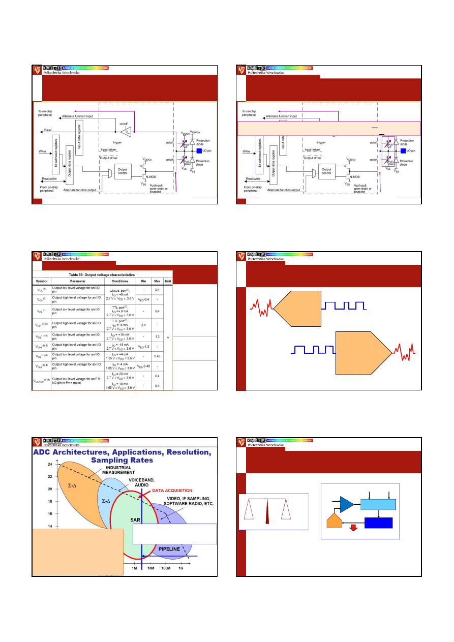
AD Converter Resolution
High Speed Data Conversion Overview.
Analog Devices, 2006, Section 1
MCU
Sigma-Delta (
ΣΣΣΣ
─
∆∆∆∆
)
Dual—Slope Integrating
Successive Approximation (SAR)
R
o
z
d
z
ie
lc
z
o
ś
ć
(
re
s
o
lu
ti
o
n
)
[b
it
y
]
Cz
ę
stotliwo
ść
próbkowania (sampling rate) [Hz]
Cztery główne segmenty rynkowe
aplikacji przetworników A/C:
zbieranie danych (Data Acquisition),
precyzyjne pomiary przemysłowe
(Precision Industrial Measurement),
aplikacje audio (Voiceband and Audio),
pomiary z wysok
ą
cz
ę
stotliwo
ś
ci
ą
próbkowania (High Speed)
Metoda kompensacyjno-wagowa
(Successive Approximation)
U
X
?
? = 11
0
1
CONTROL
LOGIC
CLOCK
START
V
IN
COMPARATOR
─
+
D/A
REGISTER
DATA OUTPUT
K. ParkikH: A/D and D/A converters trade off performance
and resolution. TI (http://www.electronicproducts.com/Analog_Mixed_Signal_ICs/
A_D_and_D_A_converters_trade_off_performance_and_resolution.aspx)
Rys. 4. Metoda kompensacyjno-wagowa zapewnia:
rozdzielczo
ść
od 8 do 14 bitów
niskie zu
ż
ycie energii
nisk
ą
pr
ę
dko
ść
próbkowania, zwykle ograniczon
ą
do 1 MPróbki / s.
3
Metoda kompensacyjno-wagowa
(Successive Approximation)
Przykład
U
X
= 13 V
FS
= 16 V, N = 4, 1LSB =
FS
/
2N
= 1 V
i = 3
U
3
(MSB) = 1/2
N - i
∗
FS = 8 V,
U
X
≥≥≥≥
(U
3
)
= 8
U
3
=
1
i = 2
U
2
= 1/2
N - i
∗
FS = 4 V,
U
X
≥≥≥≥
(U
3
+ U
2
)
= 12
U
2
=
1
i = 1
U
1
= 1/2
N - i
∗
FS = 2 V,
U
X
<
(U
3
+ U
2
+ U
1
)
= 14
U
1
= 0
i = 0
U
0
(LSB) = 1/2
N - i
∗
FS = 1 V,
U
X
≥≥≥≥
(U
3
+ U
2
+
U
1
+ U
0
)= 13
U
0
=
1
U
X
?
? = 11
0
1
K. ParkikH: A/D and D/A converters trade off performance
and resolution. TI (http://www.electronicproducts.com/Analog_Mixed_Signal_ICs/
A_D_and_D_A_converters_trade_off_performance_and_resolution.aspx)
Metoda podwójnego całkowania
(Dual—Slope Integrating)
Figure 2: Dual Slope Integrating ADC
W. Kester, J. Bryant: ADC Architectures VIII:
Integrating ADCs. (MT-027 TUTORIAL) Analog Devices, Rev.A, 10/08, fig. 2
Metoda podwójnego całkowania
(Dual—Slope Integrating)
Tłumienie zakłóceń
Figure 3: Frequency Response of Integrating ADC
excellent
rejection of
50-Hz & 60-Hz
W. Kester, J. Bryant: ADC Architectures VIII:
Integrating ADCs. (MT-027 TUTORIAL) Analog Devices, Rev.A, 10/08, fig. 3
Metoda Sigma-Delta
(
ΣΣΣΣ
─
∆∆∆∆
)
Quantization Using Delta Modulation
V
IN
1-BIT
A/D
1-BIT
D/A
CLOCK
+
K(Z)
DIGITAL
LOW-PASS FILTER/
DECIMATOR
DATA OUTPUT
K. ParkikH: A/D and D/A converters trade off performance
and resolution. TI (http://www.electronicproducts.com/Analog_Mixed_Signal_ICs/
A_D_and_D_A_converters_trade_off_performance_and_resolution.aspx)
Rys. 5. Metoda sigma-delta oferuje
rozdzielczo
ść
od 16 do 24 bitów,
najbardziej precyzyjne przetwarzanie w
ś
ród ró
ż
nych architektur,
wolniejsz
ą
prac
ę
z nisk
ą
cz
ę
stotliwo
ś
ci
ą
próbkowania (np. 48 kpróbek / s.
Tryby pracy
przetworników
(Analog Devices)
Figure 57. ADC in Single-Ended Mode
Figure 56. ADC in Pseudo
Differential Mode
Figure 55. ADC Conversion Phase
(Differential Mode)
Precision Analog Microcontroller, 12-Bit Analog I/O, ARM7TDMI
MCU . ADuC7019/20/21/22/24/25/26/27/28/29. Data Sheet Rev. F. Analog Devices.
Sprzeczności konstrukcyjne
precyzyjna analogowa struktura
przetwornika A/C pracuj
ą
ca z napi
ę
ciami
na bardzo małym poziomie, np.:
napi
ę
cie
warto
ść
1 LSB dla rozdzielczo
ś
ci
wzorcowe
V
REF
[V]
8 bitów
10 bitów
12 bitów
14 bitów
16 bitów
24 bity
[mV]
[mV]
[
µµµµ
V]
[
µ
V]
[
µ
V]
[nV]
5,0
19,6
4,89
1221
306
76,3
298
3,3
12,9
3,23
806
201
50,4
197
2,5
9,77
2,44
610
152
38,1
149
1,8
7,03
1,76
439
110
27,5
107
1,5
5,86
1,47
366
91,6
22,9
89,4
1,2
4,69
1,17
293
73,2
18,3
71,5
0,8
3,12
0,781
195
48,8
12,2
47,7
szybko działaj
ą
ca struktura cyfrowa
z napi
ę
ciami o poziomie kilka
rz
ę
dów wy
ż
szymi od cz
ęś
ci analogowej, V
CC
= 0,8 .. 5,5 V
4
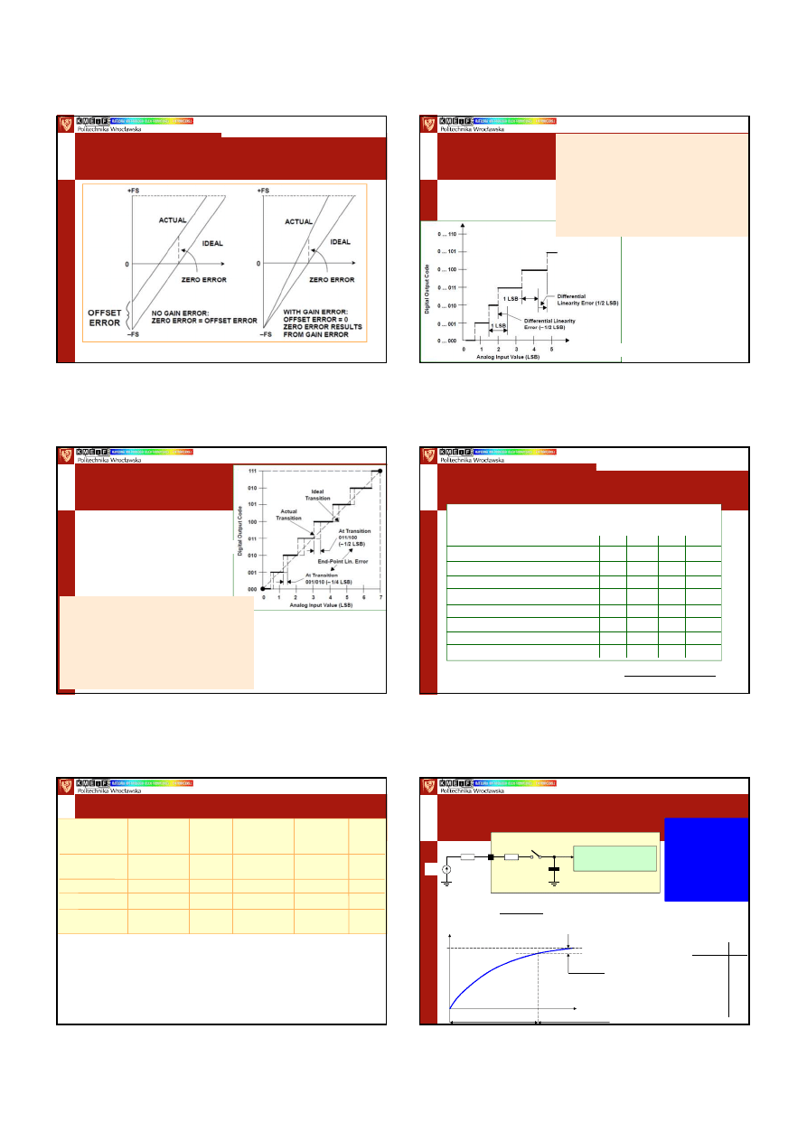
Błąd przesunięcia
(Offset Error)
Błąd nachylenia
(Gain Error)
Kester W.: The Importance of Data Converter Static
Specifications Don't Lose Sight of the Basics !
(MT-010 TUTORIAL) Analog Devices, Rev.A, 10/08
Figure 4: Bipolar Data Converter Offset and Gain Error
Błąd liniowości
(Linearity Errors)
[1#2]
Understanding Data Converters. Application Report.
SLAA013. TI, 1995
Figure 5. Differential Nonlinearity (DNL)
Bł
ą
d nieliniowo
ś
ci ró
ż
niczkowej
(Differential NonLinearity Error) – ró
ż
nica
pomi
ę
dzy rzeczywist
ą
szeroko
ś
ci
ą
kroku
przetwarzania oraz idealn
ą
warto
ś
ci
ą
1 LSB
DNL = 0, szeroko
ść
kroku przetwarzania
równa 1 LSB
DNL przekracza 1 LSB – mo
ż
liwo
ść
niemonotonicznej pracy przetwornika
Błąd liniowości
(Linearity Errors)
[2#2]
Understanding Data Converters. Application Report.
SLAA013. TI, 1995
Figure 6. Integral Nonlinearity (INL) Error
Bł
ą
d nieliniowo
ś
ci całkowej
(Integral
NonLinearity Error) – odchylenie
charakterystyki rzeczywistej od teoretycznej
charakterystyki przetwarzania
charakterystyka rzeczywista wyznaczona na
podstawie wyników kalibracji
INL wyra
ż
any w LSB
STM32L053xx
Cortex-M0+
Table 62
. ADC characteristics.
Table 64
. ADC accuracy (range 1/2/3).
Parameter
Min
Typ
Max
Unit
Sampling rate
0,05
-
1.14
MHz
Integral Nonlinearity
-
±
1.5
±
2,5
LSB
Differential Nonlinearity
-
±
1
±
1.5
LSB
Offset Error
-
±
1
±
2.5
LSB
Gain Error
-
±
1
±
2
LSB
Total harmonic distortion
-
—
85
—
73
dB
Sampling switch resistance
1
k
Ω
Internal sample and hold capacitor
8
pF
12-Bit AD Converter:
20 log (2
12
) = 72 dB
STM32L053xx. Ultra-low-power 32-bit MCU ARM
®
-based
Cortex
®
-M0+, up to 64KB Flash, 8KB SRAM, 2KB EEPROM, LCD, USB,
ADC, DAC. STMicroelectronics, September 2014
R
AIN
< – R
ADC
T
S
f
ADC
∗
C
ADC
∗
ln(2
N+2
)
Napięcie wzorcowe
(Voltage Reference)
MODEL
Output
Voltage
Temperature
Long-Term
Supply
voltage
accuracy
coefficient
stability
Current
[V]
[ppm/°C]
[ppm]
[
µ
A]
1)
ADR440B
2.048
±
1 mV
±
1
±
50
3mA
ADR444B
4.096
(25
°
)
2)
MAX6138
2.048 / 4.096
±
0.1%
±
25
±
120
45
TYP
3)
LM4132
2.048 / 4.096
±
0.05%
±
10
±
50
60
4)
REF5020I
2.048
±
0.05%
±
3
800
REF5040I
4.096
(25
°
)
1. ADR440. Ultralow Noise, LDO XFET Voltage References with Current Sink and Source.
Analog Devices, 2008, D05428-0-3/08, Rev. C
2. MAX6138. Shunt Voltage Reference with Multiple Reverse Breakdown Voltages.
Maxim, 2004, Rev 2; 4/04
3. LM4132. SOT-23 Precision Low Dropout Voltage Reference.
National Semiconductor, DS201513, August 2006
4. REF50xx Low-Noise, Very Low Drift, Precision VOLTAGE REFERENCE
Texas Instruments SBOS410D, REVISED APRIL 2009
Układ próbkująco-pamiętający
(Sample
&
Hold)
R
S
R
I
C
I
N-bitowy przetwornik
analogowo-cyfrowy
K
V
S
t
V
CI
= V
S
(1 - e )
V
S
t
SAMPLE
<
1
/
2
LSB
(R
S
+ R
I
)
∗
C
I
t
t
S
(
1
/
2
LSB) = (R
S
+ R
I
)
∗
C
I
∗
ln(2
∗
2
N
)
ln(2
∗
2
N
)
N
6,24
8
7,62
10
9,01
12
10,40
14
11,76
16
17,33
24
t
HOLD
+ t
CONVERSION
przykład:
N = 12 bitów
R
I
= 2 k
Ω
Ω
Ω
Ω
C
IMAX
= 40 pF
R
S
= 10 k
Ω
Ω
Ω
Ω
t
SAMPLE
≥≥≥≥
4,33
µµµµ
s
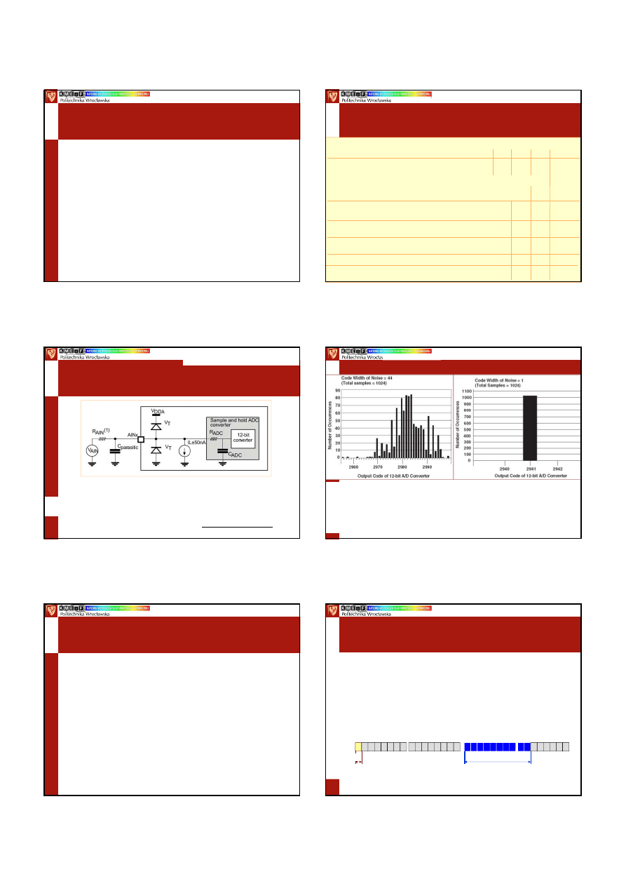
5
Wymagania Sample
&
Hold
programowalny
(zmienny)
czas próbkowania
t
SAMPLE
mała rezystancja
wej
ś
ciowego MPX i kluczy układu S&H
mała pojemno
ść
wej
ś
ciowa C
I
układu S&H
mała stratno
ść
kondensatora pami
ę
taj
ą
cego C
I
krótki czas przetwarzania
ze wzgl
ę
du na upływno
ść
kondensatora
pami
ę
taj
ą
cego C
I
małe pr
ą
dy wej
ś
ciowe
MSP430FG4618
Some ADC Parameters
12-bit ADC parameters (V
CC
= 2.2 – 3 V)
PARAM TEST /CONDITIONS
MIN NOM MAX
UNIT
t
Sampling
Sampling time / R
S
= 400
Ω
, R
I
= 1000
Ω
,
1220
ns (3V)
C
I
= 30pF,
τ
= [R
S
+ R
I
] x C
I
1440
ns (2.2V)
Approximately ten Tau (
τ
) are needed to get an error of less than ±0.5 LSB:
t
Sample
= ln(2
n+1
)
∗
(R
S
+ R
I
)
∗
C
I
+ 800 ns
where n = ADC resolution = 12, R
S
= external source resistance
E
I
Integral linearity error / 1.4 V
≤
Ve
REF+
≤
1.6 V
±2
LSB
1.6 V < Ve
REF+
≤
V
AVCC
±1.7
LSB
E
D
Differential linearity error / C
VREF+
=
10
µ
F (tantalum)
and 100nF (ceramic)
±1
LSB
E
O
Offset error / Internal impedance of source R
S
< 100
Ω
C
VREF+
=
10
µ
F (tantalum) and 100nF (ceramic)
±2
±4
LSB
E
G
Gain error / C
VREF+
=
10
µ
F (tantalum) & 100 nF (ceramic)
±1.1
±2
LSB
E
T
Total unadjusted error / C
VREF+
=
10
µ
F (tantalum)
and 100nF (ceramic)
±2
±5
LSB
MSP430xG461x. MIXED SIGNAL MICROCONTROLLER
Texas Instruments, SLAS508G, REVISED OCTOBER 2007
STM32L053
Cortex-M0+
[1#2]
Figure 27. Typical connection diagram using the ADC
STM32L053xx. Ultra-low-power 32-bit MCU ARM
®
-based
Cortex
®
-M0+, up to 64KB Flash, 8KB SRAM, 2KB EEPROM, LCD, USB,
ADC, DAC. STMicroelectronics, September 2014
Sampling switch resistance < 1 k
Ω
Internal sample and hold capacitor < 8 pF
R
AIN
< – R
ADC
T
S
f
ADC
∗
C
ADC
∗
ln(2
N+2
)
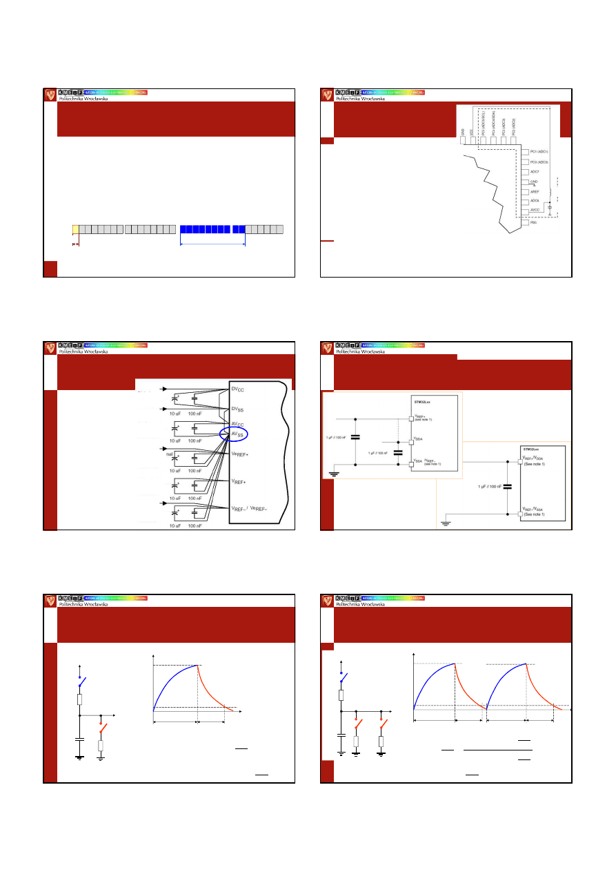
Noise
Figure 2. When low noise precautions
are not taken during circuit design
and board layout, a 12-bit ADC
system under-performs with
approximately 5.45-bit accuracy (or
5.45 Effective Number of Bits).
Figure 3. If low noise, active and
passive devices are used, a ground
plane is included, by-pass
capacitors are added and a low-
pass (anti-aliasing) filter is placed
in the signal path. The code width
of 1024 samples is equal to one.
Bonnie C. Baker: Techniques that Reduce System
Noise in ADC Circuits. Microchip Technology, Analog Design Note ADN007
ATmega8
The
ADC
features a
noise canceler
that enables conversion during sleep
mode to reduce noise induced from the CPU core and other I/O
peripherals. The noise canceler can be used with ADC Noise Reduction
and Idle mode. To make use of this feature, the following procedure should
be used:
Make sure that the ADC is enabled and is not busy converting.
Single
Conversion mode must be selected and the ADC conversion
complete interrupt must be enabled
.
Enter ADC Noise Reduction mode (or Idle mode).
The ADC will start a
conversion once the CPU has been halted
.
If no other interrupts occur before the ADC conversion completes, the
ADC interrupt will wake up the CPU
and execute the ADC
Conversion Complete interrupt routine.
ATmega8. 8-bit with 8K Bytes
In-System Programmable Flash. Atmel 2002, Rev. 2486H–AVR–09/02
LPC21xx:
10-bit successive approximation
ARM7
ADC Data Register
(ADDR – RW, undefined)
–
LPC213x
ADC Global Data Register
(AD0GDR, AD1GDR)
–
LPC214x
Converter0: AD0DR - 0xE003 4004
Converter0: AD1DR - 0xE006 0004
contains the ADC’s
DONE
bit and (when DONE is 1) the 10-bit result of the
most recent A/D conversion
ADDR / ADGDR
(ADC Data Register):
15
0
DATA
5
? ? ? ? ?
6
x x x x x x
x x x x
? ? ? ?
? ? ? ?
? ? ? ?
0
0 ? ?
16
23
24
26
31
?
DONE
while ( ~ADDR & 0x8000 0000);
// end of conversion ?
result = (ADDR & (0x3FF << 6)) >> 6;
// result calculation
UM10120. LPC2131/2/4/6/8 User manual.
NXP, Rev. 02 - 25 July 2006
6
LPC1114:
10-bit successive approximation
Cortex-M0
AD0GDR / AD0DRn
(ADC Data Register):
15
0
DATA
5
? ? ? ? ?
6
x x x x x x
x x x x
? ? ? ?
? ? ? ?
? ? ? ?
0
0 ? ?
16
23
24
26
31
?
DONE
while ( ~ADGDR & 0x8000 0000);
// end of conversion ?
result = (ADGDR & (0x3FF << 6)) >> 6;
// result calculation
UM10398. LPC111x/LPC11Cxx User manual.
NXP, Rev. 12.3 — 10 June 2014
ADC Global Data Register
(AD0GDR)
A/D Channel 0 Data Register (AD0DR0) ...
... A/D Channel 7 Data Register (AD0DR7)
contains the ADC’s
DONE
bit and (when DONE is 1) the 10-bit result of the
most recent A/D conversion
ATmega8
PCB
Analog Noise Canceling Techniques
:
Keep
analog signal paths as short
as
possible. Make sure analog tracks run
over the analog ground plane, and
keep
them
well
away from high-speed
switching digital tracks
.
A
VCC
pin on the device should be
connected to the digital
VCC supply
voltage via an LC network
Use
ADC noise canceler
function to reduce induced noise from the CPU
If any ADC port pins are used as
digital outputs
, it is essential that these
do
not switch while a conversion is in progress
100nF
10
µ
H
A
n
a
lo
g
G
ro
u
n
d
P
la
n
e
ATmega8. 8-bit with 8K Bytes
In-System Programmable Flash. Atmel 2002, Rev. 2486H–AVR–09/02
MSP430
PCB
MSP430xG461x. MIXED SIGNAL MICROCONTROLLER
Texas Instruments, SLAS508G, REVISED OCTOBER 2007
Digital Power
Supply Decoupling
Analog Power
Supply Decoupling
Using an External
Positive Reference
Using the Internal
Reference Generator
Using an External
Negative Reference
STM32L053
Cortex-M0+
[2#2]
STM32L053xx. Ultra-low-power 32-bit MCU ARM
®
-based
Cortex
®
-M0+, up to 64KB Flash, 8KB SRAM, 2KB EEPROM, LCD, USB,
ADC, DAC. STMicroelectronics, September 2014
Figure 29. Power supply and
reference decoupling
(V
REF+
connected
to V
DDA
)
Figure 28. Power supply and
reference decoupling
(V
REF+
not connected
to V
DDA
)
Multi—Slope ADCs
[1#3]
R
1
C
V
CC
t
V
C
V
CC
Phase 1
t
1
= –R
2
∗
C
∗
ln = N
∗
t
CLK
V
C
R
2
K
2
K
1
Charge
C
K1 - ON
K2 - OFF
V
REF
Phase 2
Discharge
C
K1 - OFF
K2 - ON
t
1
V
REF
V
CC
N = –R
2
∗∗∗∗
C
∗∗∗∗
f
CLK
∗∗∗∗
ln
V
REF
V
CC
MSP430x4xx Family. User’s Guide. Mixed Signal Products.
Texas Instruments SLAU056C, 2003
Multi—Slope ADCs
[2#3]
R
1
C
V
CC
t
V
C
V
CC
Phase 1
V
C
R
2
K
2
K
1
Charge
C
K1 - ON
K2 - OFF
K4 - OFF
V
REF
Phase 2
Discharge
C
K1 - OFF
K2 - ON
K4 - OFF
t
1
–R
4
∗
C
∗
f
CLK
∗
ln
V
REF
V
CC
R
4
K
4
Phase 3
Charge
C
K1 - ON
K2 - OFF
K4 - OFF
Phase 4
Discharge
C
K1 - OFF
K2 - OFF
K4 - ON
t
4
–R
2
∗
C
∗
f
CLK
∗
ln
V
REF
V
CC
N
4
N
2
=
N
4
N
2
R
4
= R
2
7
Multi—Slope ADCs
[3#3]
To get a resolution of N bits, the capacitor C must have a minimum capacity:
–2
N
R
XMIN
∗∗∗∗
f
CLK
∗∗∗∗
ln
C >
V
REFMAX
V
CC
f
CLK
measurement frequency in Hertz
R
XMIN
lowest resistance of sensor or reference resistor in Ohms
V
REFMAX
maximum value for threshold voltage V
REF
in Volts
MSP430
GPIO
&
Comparator
Temperature Measurement System
MSP430x4xx Family. User’s Guide. Mixed Signal Products.
Texas Instruments SLAU056C, 2003
Figure 1: 1-Bit DAC:
Changeover
Switch (Single-
Pole, Double
Throw, SPDT)
Simplest DAC Architectures
Kester W.: Basic DAC Architectures I: String DACs and
Thermometer (Fully Decoded) DACs. Analog Devices, 2008, MT-014 TUTORIAL, Rev.A, 10/08
R-2R Network DAC
Architectures
Figure 5: Voltage-Mode R-2R Ladder Network DAC
Kester W.: Basic DAC Architectures I: String DACs and
Thermometer (Fully Decoded) DACs. Analog Devices, 2008, MT-014 TUTORIAL, Rev.A, 10/08
12-bit DA Converters
C8051F00x
D
11
D
10
D
9
D
8
D
7
D
6
D
5
D
4
D
3
D
2
D
1
D
0
-
-
-
-
D
11
D
10
D
9
D
8
D
7
D
6
D
5
D
4
D
3
D
2
D
1
D
0
-
-
-
-
1xx
010
D
11
D
10
D
9
D
8
D
7
D
6
D
5
D
4
D
3
D
2
D
1
D
0
-
-
-
-
000
DAC0L (0D2h)
DAC1L (0D5h)
DAC0H (0D3h)
DAC1H (0D6h)
DACx
DACx
V
DD
DACxEN
.....
.....
V
REF
Data is latched into DAC0 after a write to the corresponding DAC0H
register, so the write sequence should be DAC0L followed by DAC0H if the
full 12-bit resolution is required.
C8051F00x/1/2/5/6/7. Mixed-Signal 32KB ISP
FLASH MCU Family. Silicon Laboratories, 2003, Rev. 1.7 11/03
STM32F05xxx
(Cortex-M0)
Digital-to-analog converter
RM0091. Reference manual. STM32F05xxx advanced
ARM-based 32-bit MCUs. STMicroelectronics, August 2012
voltage output 12-bit digital-to-analog converter
configured in 8- or 12-bit mode and may be used in conjunction with the DMA
controller
In 12-bit mode, the data could be left- or right-aligned, three possibilities:
– 8-bit right alignment: data into the DAC_DHR8Rx[7:0] bits
– 12-bit left alignment: data into the DAC_DHR12Lx[15:4] bits
– 12-bit right alignment: data into the DAC_DHR12Rx[11:0] bits
Available input
reference voltage, V
DDA
External triggers
for conversion
ADC output optionally buffered for higher current drive
8
STM32F05xxx
(Cortex-M0)
Digital-to-analog converter
Buffered output
RM0091. Reference manual. STM32F05xxx advanced
ARM-based 32-bit MCUs. STMicroelectronics, August 2012
AN4058. Audio and waveform
generation using the DAC in
STM32F0xx microcontroller
families. Application note.
STMicroelectronics, 2 may 2012
przetwornik DAC posiada wewn
ę
trzny wzmacniacz operacyjny, który mo
ż
na
wł
ą
cza
ć
i wył
ą
cza
ć
w zale
ż
no
ś
ci od aplikacji u
ż
ytkownika (brak zewn
ę
trznego
wzmacniacza wyj
ś
ciowego)
przykład sygnału sinusoidalnego
: 10 próbek dla pojedynczego okresu
sygnału (0 .. 2
∗Π
)
STM32F05xxx
(Cortex-M0)
Digital-to-analog converter
[1#4]
STM32F051x4/6/8. Low- and medium-density advanced
ARM™-based 32-bit MCU with 16 to 64 Kbytes Flash, timers,
ADC, DAC and comm. Interfaces. Data sheet.
STMicroelectronics, 23 July 2012
Table 57. DAC characteristics
Symbol Parameter
Min Typ Max Unit Comments
R
LOAD
(1)
Resistive load with
5
-
-
k
Ω
Load is referred to ground
buffer ON
R
O
(1)
Impedance output with
-
-
15 k
Ω
When the buffer is OFF,
buffer OFF
the Minimum resistive
load between DAC_OUT
and VSS to have a 1%
accuracy is 1.5 M
Ω
I
DDA
DAC DC current
-
-
380
µ
A
With no load, middle code
consumption in
(0x800) on the input
quiescent mode
With no load, worst code
(Standby mode)
-
-
480
µ
A
(0xF1C) on the input
Table 33. Peripheral current consumption
Peripheral
Typical consumption at 25 °C
Unit
I
DD
I
DDA
DAC
0.27
0.408
mA
STM32F05xxx
(Cortex-M0)
Digital-to-analog converter
[2#4]
STM32F051x4/6/8. Low- and medium-density advanced
ARM™-based 32-bit MCU with 16 to 64 Kbytes Flash, timers,
ADC, DAC and comm. Interfaces. Data sheet.
STMicroelectronics, 23 July 2012
Table 57. DAC characteristics
Symbol Parameter
Min Typ Max Unit Comments
DNL
Differential non
-
-
±0.5 LSB
Given for the DAC in
linearity between
10-bit configuration
two consecutive
-
-
±2 LSB Given for the DAC in
code-1LSB
12-bit configuration
INL
Integral non linearity
(difference between
-
-
±1 LSB Given for the DAC in
measured value at
10-bit configuration
Code i and the value
at Code i on a line
-
-
±4 LSB Given for the DAC in
drawn between Code 0
12-bit configuration
and last Code 1023)
Offset
Offset error
-
-
±10 mV
Given for the DAC in
(difference between
12-bit configuration
measured value at
-
-
±3 LSB Given for the DAC in
Code (0x800) and the
10-bit at V
DDA
= 3.6 V
ideal value = V
DDA
/2)
-
-
±12 LSB Given for the DAC in
12-bit at V
DDA
= 3.6 V
STM32F05xxx
(Cortex-M0)
Digital-to-analog converter
[3#4]
STM32F051x4/6/8. Low- and medium-density advanced
ARM™-based 32-bit MCU with 16 to 64 Kbytes Flash, timers,
ADC, DAC and comm. Interfaces. Data sheet.
STMicroelectronics, 23 July 2012
Table 57. DAC characteristics
Symbol Parameter
Min Typ Max Unit Comments
Gain
Gain error
-
-
±0.5 %
Given for the DAC in
12bit configuration
t
SETTLING
Settling time
(full scale: for a 10-bit
input code transition
-
3
4
µ
s
C
LOAD
≤
50 pF,
between the lowest
R
LOAD
≥
5 k
Ω
and the highest input
codes when DAC_OUT
reaches final value
±1LSB
Update Max frequency for
rate
(2)
a correct DAC_OUT
-
-
1
MS/s C
LOAD
≤
50 pF,
change when small
R
LOAD
≥
5 k
Ω
variation in the input
code (from code i to
i+1LSB)
STM32F05xxx
(Cortex-M0)
Digital-to-analog converter
[4#4]
STM32F051x4/6/8. Low- and medium-density advanced
ARM™-based 32-bit MCU with 16 to 64 Kbytes Flash, timers,
ADC, DAC and comm. Interfaces. Data sheet.
STMicroelectronics, 23 July 2012
Table 57. DAC characteristics
Symbol Parameter
Min Typ Max Unit Comments
t
WAKEUP
(2)
Wakeup time from off
-
6.5 10
µ
s
C
LOAD
≤
50 pF,
state (Setting the ENx
R
LOAD
≥
5 k
Ω
bit in the DAC Control
input code between lowest
highest possible ones.
(1)
Guaranteed by design, not tested in production.
(2)
Data based on characterization results, not tested in production
PWM
[1#2]
V
C
t
τ
T
0,
0
≤
t < T -
τ
V
C
,
T -
τ ≤
t < T
U(t) =
U(t)
{
Warto
ść
ś
rednia: U
sr
=
T
1
U(t) dt = V
C
∗
∫
0
T
T
τ
9
PWM
[2#2]
B = 0
B = 1
B = 2
B = 3
B = 4
B = 5
B = 6
B = 7
A0 A1 A2
C0 C1 C2
Licznik
B0
B1
B2
A < B
R
e
je
s
tr
P
W
M
komparator
C = 0
A = 0
1
1
2
2
3
3
4
4
5
5
6
6
7
7
Licznik
Komparator
DPM - Distributed Pulse Modulation
np. P82C150 SLIO (Philips)
C = 0
A = 0
1
4
2
2
3
6
4
1
5
5
6
3
7
7
B = 0
B = 1
B = 2
B = 3
B = 4
B = 5
B = 6
B = 7
A0 A1 A2
C0 C1 C2
Licznik
B0
B1
B2
A < B
R
e
je
s
tr
P
W
M
komparator
Licznik
Komparator
Źródło prądowe
zmienne obci
ąż
enie R
VAR
i rezystor wzorcowy R
REF
warto
ść
pr
ą
du obci
ąż
enia I
L
:
programowa modulacja szeroko
ś
ci impulsów aby V
AC
= V
COMPREF
I
L
=
∗
V
CC
R
REF
R
2
R
1
+ R
2
we A/C
wy PWM
V
CC
AV
REF
AV
SS
V
SS
COMPREF
+
–
R
REF
R
VAR
R
2
R
1
Problemy i pytania
1. Jakie cechy charakteryzuj
ą
przetworniki analogowo-cyfrowe (A/C) ?
2. Jak definiowana jest warto
ść
1 LSB ?
3. Jak opisa
ć
zasad
ę
‘sukcesywnej aproksymacji’ dla przetworników A/C ?
4. Na czym polega metoda ‘podwójnego całkowania’ przetworników A/C ?
5. W jakich sytuacjach metoda ‘podwójnego całkowania’ nie zdaje egzaminu ?
6. Jakie typy bł
ę
dów charakteryzuj
ą
przetworniki A/C ?
7. Jakie s
ą
spotykane formy zapisu 12-bitowych wyników przetwarzania ?
8. Jakie zasady obowi
ą
zuj
ą
przy projektowaniu płytek drukowanych dla
mikrokontrolerów z przetwornikami A/C ?
9. Jak redukowa
ć
zakłócenia pogarszaj
ą
ce dokładno
ść
przetwarzania
przetworników A/C ?
10. Na czym polega metoda wielokrotnego całkowania ?
11. Jakie parametry charakteryzuj
ą
działanie przetworników C/A ?
12. W jaki sposób mo
ż
na generowa
ć
sygnały analogowe w mikrokontrolerach ?
13. Jakie jest zastosowanie metody PWM w
ź
ródłach pr
ą
dowych ?
Wyszukiwarka
Podobne podstrony:
więcej podobnych podstron