
770
Service Manual

TABLE OF CONTENTS
S
E
R
V
I
C
E
WARNING
· · · · · · · · · · · · · · · · · · · · · · · · · · · · · · · · · · · · · · · · · · · · · · · · ·
1
A. IMPORTANT SAFETY INSTRUCTION
· · · · · · · · · · · · · · · · · · · · ·
1
B. SPECIFICATIONS
· · · · · · · · · · · · · · · · · · · · · · · · · · · · · · · · · · · · · · ·
·
·
2
C. TIMING CHART
· · · · · · · · · · · · · · · · · · · · · · · · · · · · · · · · · · · · · ·
3
D. CONTROL LOCATION
· · · · · · · · · · · · · · · · · · · · · · · · · · · · · · · · ·
5
E. C
O
N
D
U
C
T
I
O
N
V I E W
· · · · · · · · · · · · · · · · · · · · · · · · · · · · · · · · · · · · · · · ·
7
F. ADJUSTMENT PROCEDURE
· · · · · · · · · · · · · · · · · · · · · · · · · · · · · · ·
1
2
G. TROUBLE SHOOTING HINTS
· · · · · · · · · · · · · · · · · · · · · · · · · · ·
13
H. REPLACEMENT PARTS LIST
· · · · · · · · · · · · · · · · · · · · · · · · · · ·
17
I. BLOCK DIAGRAM
· · · · · · · · · · · · · · · · · · · · · · · · · · · · · · · · · · · · · ·
2
7
J. SCHEMATIC DIAGRAM
· · · · · · · · · · · · · · · · · · · · · · · · · · · · · · · ·
28

WARNING
To prevent from fire or shock hazard,do not expose monitor to any rain or any form of water.High voltage is
inside the monitor so please do not remove the back cover of the cabinet if you are not a qualified
monitor engineer.Contact the local dealer or the nearest Proview branch office if you need help.
A. IMPORTANT SAFETY INSTRUCTION
Prior to using this service manual,please ensure that you have carefully followed all the procedures outlined in
the user's manual for this product.
1. Read all of these instructions.
2. Save these instructions.
3. Follow all warnings and instructions a marked on the product.
4. Unplug this product from the wall outlet before cleaning.Do not use liquid cleaners or aerosol
cleaners, use a damp cloth for cleaning.
5. Do not use this product near water.
6. Do not place this product on an unstable cart,stand or tablle.The product may fall,causing serious
damage to the product.
7. Slots and openings in the cabinet and the back or bottom are provided for ventilation,to ensure
reliable operation of the product and to protect it from overheating,those openings must not be
blocked or covered.The openings should never be blocked by placing the product on a bed,sofa, rug,
or other similar surface.This product should not be placed in a built-in installation less proper
ventilation is provided.
8. This products should be operated from the type of power source indicated on the marketin label.
If you are not sure of the type of power available, consult your dealer or local power company
9. This product is equipped with a 3-wire grounding type plug,a plug having a third (grounding)
pin.This plug will only fit into a grounding-type power outlet.This is a safety feature,if you are
unable to insert the plug into the outlet,contact your electrician to replace your obsolete outlet.Do
not defeat the purpose of the grounding-type plug.
10. Do not allow anything to rest on the power cord.Do not locate this product where persons will walk
on the cord.
11. If an extension cord is used with this product,make sure that the total of the ampere ratings on the
product plugged into the extension cord to the waplugged into outlet does not exceed 15 ampere.
12. Never push objects of any kind into this product through cabinet slots as they may touch dangerous
voltage points or short out parts that could result in a risk of fire or electric shock.Never spill liquid
of any kind on the product.
13. Do not attempt to service this product yourself,as opening or removing covers may expose you to
dangerous voltage points or other risks.Refer all servicing to service personnel.
14. Unplug this product from the wall outlet and refer servicing to qualified service personnel under the
following conditions.
a. When the power cord or plug is damaged or frayed.
b. If liquid has been spilled into the product.
c. If the product has been exposed to rain or water.
d. If the product does not operate normally,when the operating instructions are followed.Adjust
only those controls that are covered by the operating instructions since improper adjustment of

other controls may result in damage and will often require extension work by a qualified
technician to restore the product to normal operation.
e. If the product has been dropped or the cabinet has been damaged.
f.
If the product exhibits a distinct change in performance,indicating a need for service.
B. SPECIFICATIONS
1. Maximum Resolution
1280 x 1024 @ 75Hz
2. Recommend Resolution
1280 x 1024 @ 60Hz
3. Synchronization Range
Horizontal
Vertical
30 – 81 KHz
56– 75 Hz
4. Active Display Area
337mm (H) x 270mm (V)
5. Dot Pitch
0.264(H) x 0.264(V) mm
6. Support display colors
16.7M color
7. Contrast Ratio (Typical)
400
8.Luminance of White
250cd/m²
9. Bandwidth
135MHz
10. User Control
4 Key Switch
11. OSD Function
Brightness, Conrast, H-Pos, V-Pos, H. Size, Phase, Color Select,
Auto, Reset, Language, OSD Adjust, Exit
12. View Angle
Horizontal
Vertical
60 , 60 Degrees
40 , 60 Degrees
13. Power Source
100 – 240 Vac 60 / 50 Hz
14. Power Consumption
48W (max.)
15. Connection Type
15 Pin D Type
16. Input Signal
Video
Sync.
Analog R.G.B. , 0.7Vp-p / 75 Ohms
TTL level,positive or negative polarity
17. Color Temperature
Cool / Warm
18. Dimension (WxHxD)
480mm x 435mm x 180mm
19. Monitor Weight
4.2Kg
20. Base Operation
Tilt
0 / + 15 degree
21. Power Saving
ON
STAND BY
OFF
<
48W
<
5W
<
5W
22. Signal Connector Pin Assignment
Pin No.
1. Red 9. 5V
DC
2. Green 10. Sync. Ground
3. Blue 11. Ground
4. Ground 12. SDA (For DDC)
5. Self Test 13. Horizontal Sync.
6. Red Ground 14. Vertical Sync.
7. Green Ground 15. SCL (For DDC)
8. Blue Ground
23. Audio signal
3.5Φ stereo phone jack
Input Sensitivity : 200mV
2+2W 8Ω Speaker
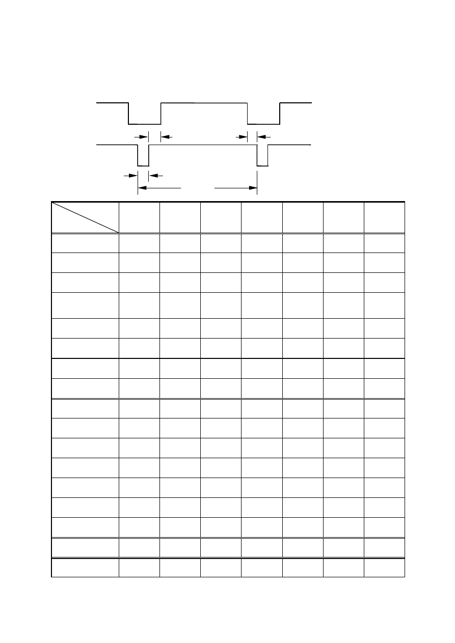
C.TIMING CHART
Video
Back porch Active display Front porch
Sync.
Sync-width
Total
Preset
Modes
VGA
720X400
VGA
640X480
VESA
640X480
VESA
640X480
VESA
800X600
VESA
800X600
VESA
800X600
Pixel clock
(MHz)
28.325 25.175 31.500 31.500 36.000 40.000 50.000
H-Frequency
(KHz)
31.472 31.469 37.861 37.500 35.156 37.879 48.077
H-Total
(
µ
s)
31.774 31.778 26.413 26.667 28.444 26.400 20.800
H-Active Display (µs)
25.419 25.422 20.317 20.317 22.222 20.000 16.000
H-Blanking (µs)
6.355 6.356 6.095 6.349 6.222 6.400 4.800
Front Porch (µs)
0.635 0.636 0.762 0.508 0.667 1.000 1.120
H-Sync-width (µs)
3.813 3.813 1.270 2.032 2.000 3.200 2.400
H-Back Porch (µs)
1.906 1.907 4.063 3.810 3.556 2.200 1.280
V-Frequency
(Hz)
70.1 59.94 72.81 75.0 56.25 60.3 72.2
V-Total
(ms)
14.267 16.683 13.735 13.333 17.778 16.579 13.853
V-Active Display (ms)
12.710 15.253 12.678 12.800 17.067 15.840 12.480
V-Blanking (ms)
1.557 1.430 1.057 0.533 0.711 0.739 1.373
V-Front Porch (ms)
0.413 0.318 0.238 0.027 0.028 0.026 0.770
V-Sync-width (ms)
0.064 0.064 0.079 0.080 0.057 0.106 0.125
V-Back Porch (ms)
1.080 1.049 0.740 0.427 0.626 0.607 0.478
H/V Sync. Polarity
-
+
-
-
-
-
-
-
+
+
+
+
+
+
Interlace
NONE NONE NONE NONE NONE NONE NONE
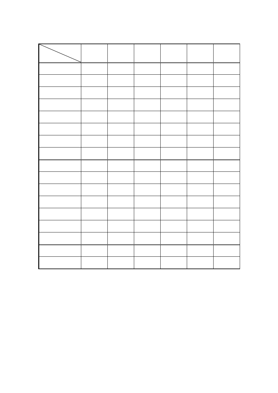
Preset
Modes
VESA
800X600
VESA
1024X768
VESA
1024X768
VESA
1024X768
VESA
1280X1024
VESA
1280X1024
Pixel clock (MHz)
49.500 65.000 75.000 78.750 108.00 135.00
H-Frequency (KHz)
46.875 48.363 56.476 60.023 63.981 97.976
H-Total (µs)
21.333 20.677 17.707 16.660 15.630 12.540
H-Active Display (µs)
16.162 15.754 13.563 13.003 11.852 9.481
H-Blanking (µs)
5.172 4.923 4.053 3.657 3.778 3.022
Front Porch (µs)
0.323 0.369 0.320 0.203 0.444 0.119
H-Sync-width (µs)
1.616 2.092 1.813 1.219 1.037 1.067
H-Back Porch (µs)
3.232 2.462 1.920 2.235 2.296 1.837
V-Frequency (Hz)
75.0 60.0 70.1 75.0 60.0 75.0
V-Total (ms)
13.333 16.666 14.272 13.328 16.661 13.329
V-Active Display (ms)
12.800 15.880 13.599 12.795 16.005 12.804
V-Blanking (ms)
0.533 0.786 0.673 0.533 0.656 0.525
V-Front Porch (ms)
0.021 0.062 0.053 0.017 0.016 0.013
V-Sync-width (ms)
0.064 0.124 0.106 0.050 0.047 0.038
V-Back Porch (ms)
0.448 0.600 0.513 0.466 0.594 0.475
H/V Sync. Polarity
+
+
-
-
-
-
+
+
+
+
+
+
Interlace
NONE NONE NONE NONE NONE NONE
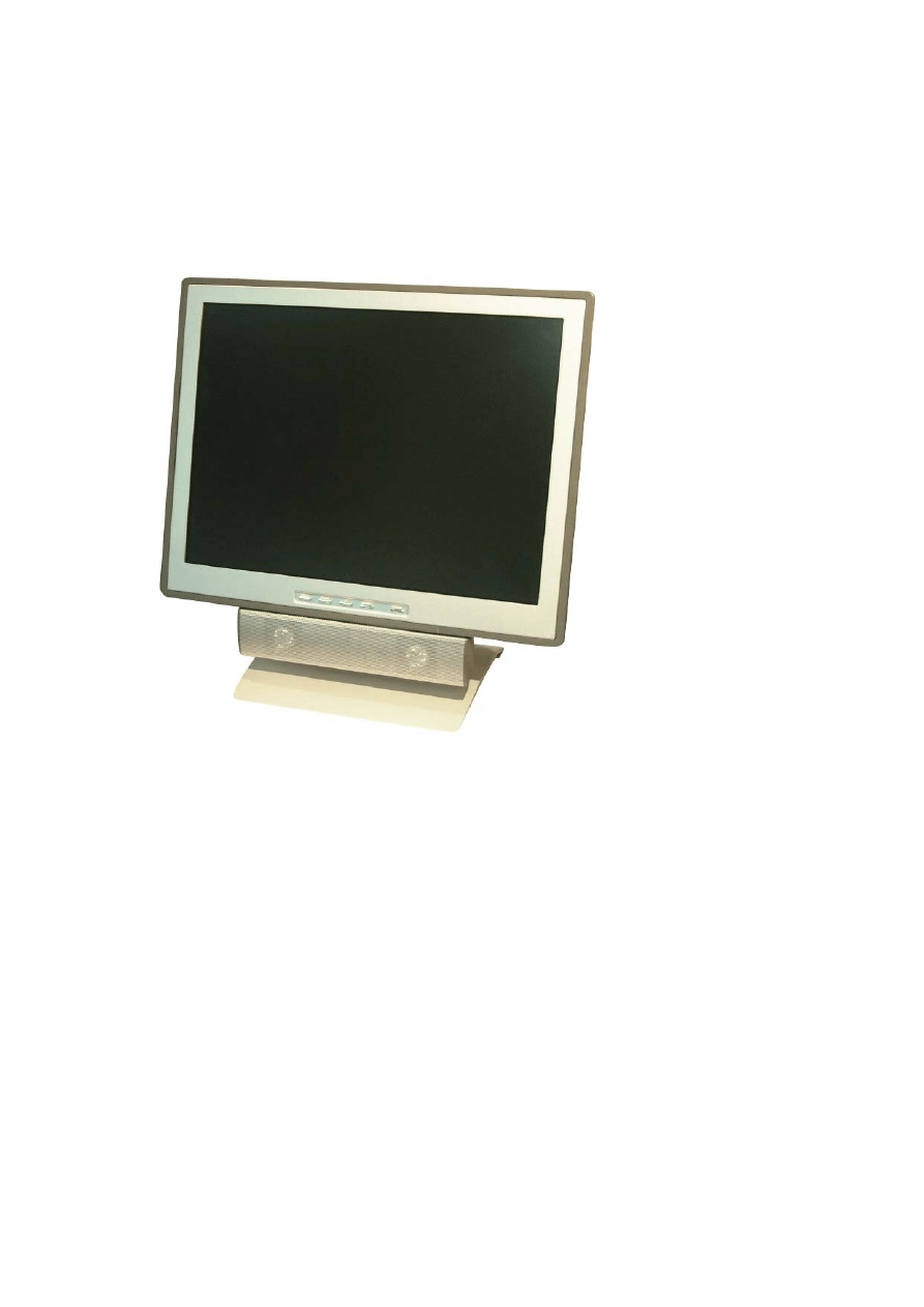
D. CONTROL LOCATION
Font control panel
1. Menu Button
2. Select Button
3. Auto Button
4. Power Button
5. LED (Power Display)
Rear panel
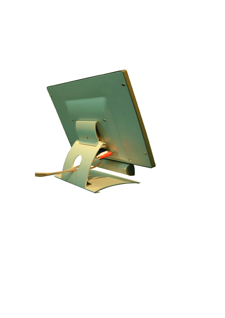
1. VGA Signal Cable
2. Power jack
3. Line in jack

E. CONDUCTION VIEW
MAIN BOARD (Component Side)
MAIN BOARD (Component Side)
MAIN BOARD (Solid Side)
CONTROL BOARD (Component Side)
CONTROL BOARD (Solid Side)
INVERTER BOARD
F. ADJUSTMENT PROCEDURE
ITEM
Program Menu.
﹟Test Meter
﹡Test Point
﹫Pattern
Operation
Check
Value
A
B+
Check
﹟Digital Voltmeter
﹡CN7
﹫Crosshatch Pattern
(31.5KHz,640x480)
1. Plug power cable into the adapter, check adapter
power indicator light up green.
2. Make sure the voltage of the power plug (
CN7
)
on the main
PCB
to the value shown at right.
12.0V
±0.2V
B
Power Saving
Check
﹟Wattmeter
﹟PC or Pattern
generator
﹫Crosshatch Pattern
(31.5KHz,640x480)
1. Unplug the signal cable into the monitor.
2. Turn the power switch of the monitor
ON
.
3. Check monitor power indicator light up orange.
4. Make sure the wattmeter value shown at right.
5.
OSD
will be display “
NO SIGNAL
” Picture.
‹ 2.5W
C
Into Factory
mode
﹟PC or Pattern
generator
﹫Crosshatch Pattern
(31.5KHz,640x480)
1. Hold ‹ key,then turn the power switch of the
monitor
OFF
.
2. Hold › key,then turn the power switch of the
monitor
ON
.
3. You can into factory adjustment mode.
D
Auto mode
Check
﹟PC or Pattern
generator
﹫Crosshatch Pattern
(1024x768/60Hz)
1. Press and relese the
MENU
knob to activate the
OSD
menu.
2. Move the
OSD
to the
AUTO
function,press
MENU
key auto adjuat display mode to its utmost
performance according to
VGA
setting.
3. In the event of the display image needs further
adjustment
E
White
Balance
Adjust
﹟
PC or Pattern
generator
﹫White Pattern
(1024x768/60Hz)
1. Move the
OSD
to the
COLOR mode
(
AUTO COLOR).
2. set color is 9300
°K
using the
OSD
,Check the value
shown at right.
Y = 220±0.1FL x = 0.283±0.01 y = 0.297±0.01
3. set color is 6500
°K
using the
OSD
,Check the value
shown at right.
Y = 220±0.1FL x = 0.313±0.01 y = 0.329±0.01
F
OSD
Language
Setting
﹟
PC or Pattern
generator
1. Move the
OSD
to the
LANGUAGE mode
.
2. You can choose one of the eight language you need.
G. TROUBLE SHOOTING HINTS
NO NO
YES YES
YES
YES
NO
NO
High Voltage !
NO
YES
YES
NO
NO
YES
No Display
( Black )
LED ON
?
Push the power
ON/OFF
switch
LED Color
change ?
Check main
board U2/Pin2
Hi / Lo under
push power
sw?
Back light
ON?
To Step 2
Make sure the
connection of
Inverter is fine
+12V ?
Check the
CN1
/Pin1
of Inverter
Check
F1(Fuse) of inverter
B
Display ?
Nice Job !
A
To Step 2
Power
adapter ?
Change
adapter
NO
YES
YES
NO
YES
NO
B
Hi / Lo under
push power
sw?
Change the
Inverter
Display ?
Nice Job !
To Step 2
A
Check the
connection of
CN8
cable
Display ?
Nice Job !
Change the
main board
Change the
main board
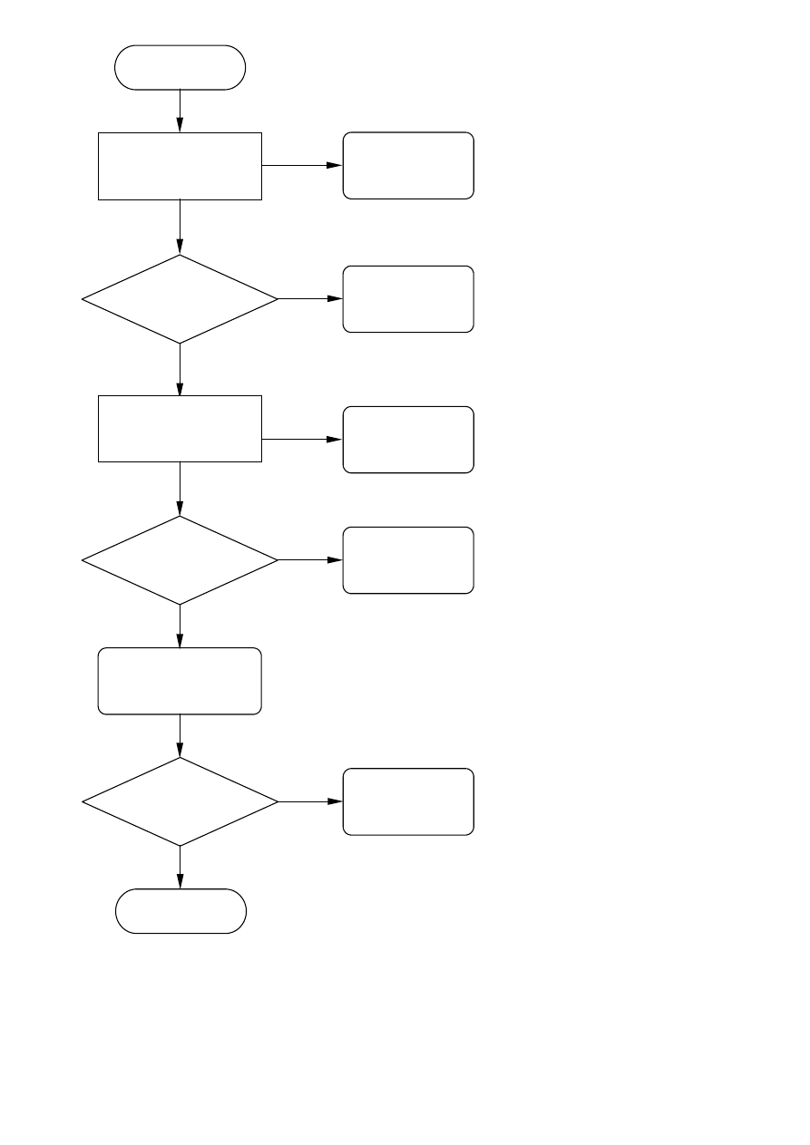
NO
YES
NO
YES
YES
YES
YES
NO
NO
YES
Step 2
Check the main
board
12V
?
+5.0 V ?
Check
U10,U11,TR1
H/V input
Signal ?
Check the main
board
U7
/
Pin 5
?
Change
U9
Check
H/V Signal
Display ?
Nice Job !
Change
Signal Cable
Check
F1,D5
Check
U7
NO
YES
NO
YES
NO
YES
YES
NO
NO
YES
No display
(White)
Check the main
board
5V
?
+3.3V ?
H/V Input
Signal ?
Check the main
board
U9/Pin3
?
Change
U9
Check
H/V Signal
Display ?
Nice Job !
Change
Signal Cable
Check
U10,U11,TR1
Check
U8,U13
Check
3.3V Circuit

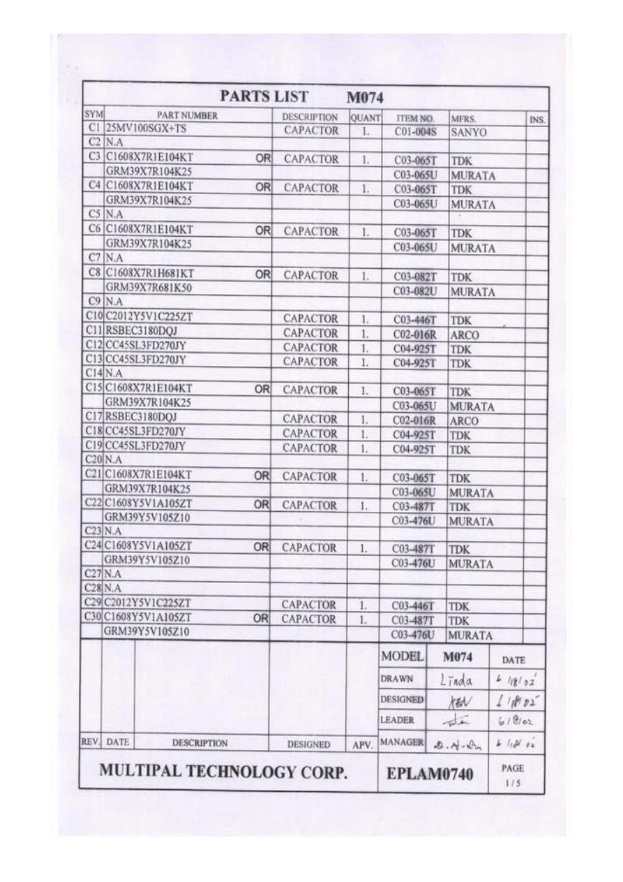
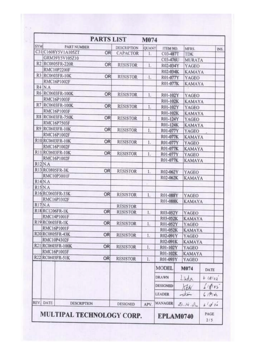
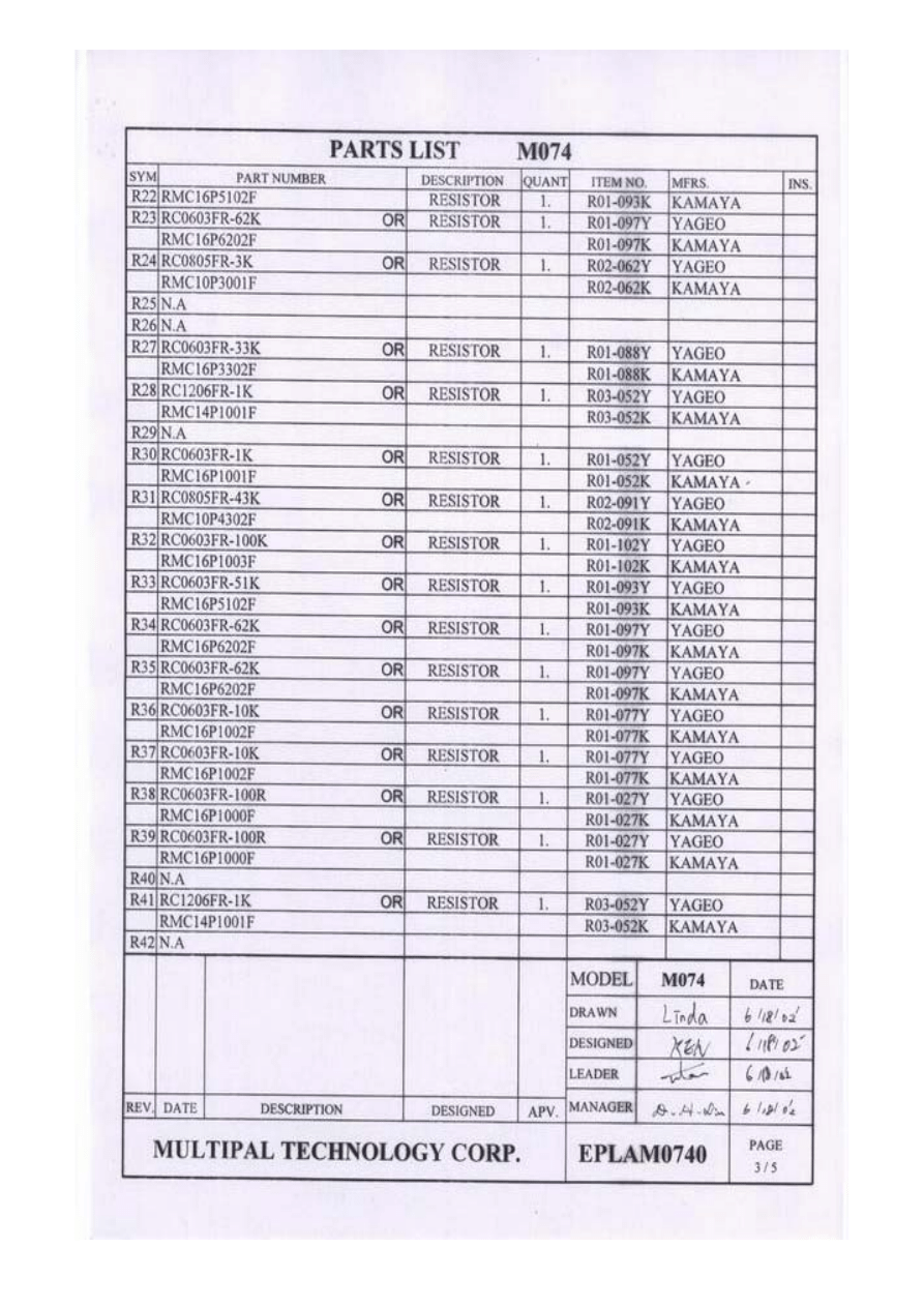
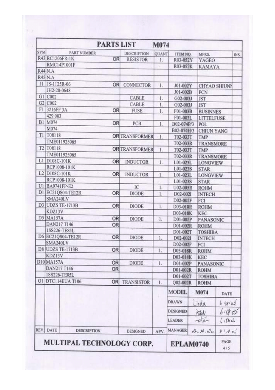
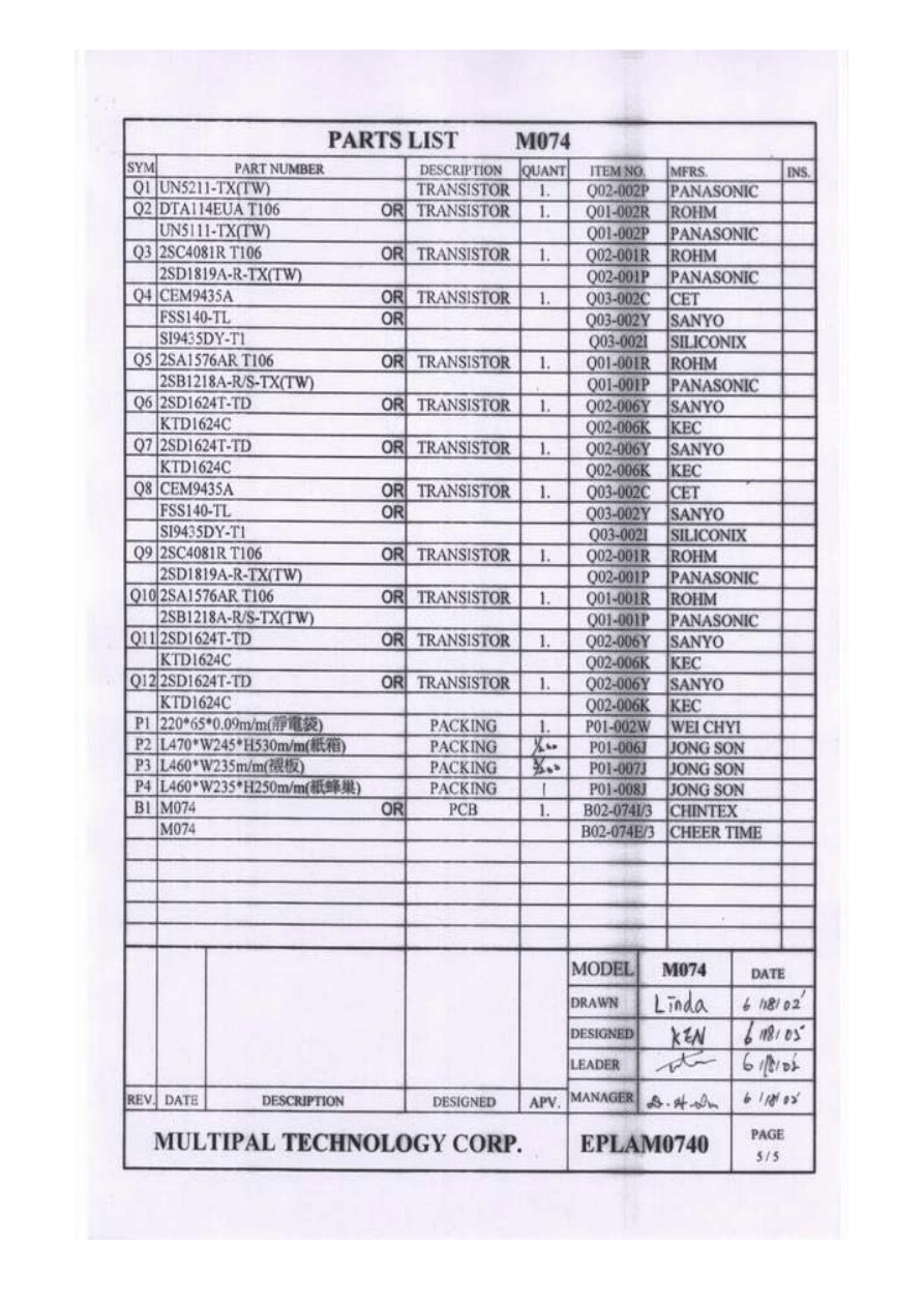
H. REPLACEMENT PARTS LIST
770
NO
Parts No.
Description
Part Location
Q’ty
1 988-1L0-6001C
SH770
2 002-001-CEPOV-A CE Declaration
1
3 002-G01-FUJIT
FUJITSU Warranty card
1
4 002-L03-FUJIT
SH770 User’s Manual for FUJITSU
1
5 003-101-TCO9
All Series TCO99 Label for Carton
1
6 003-403-FUJIT
SH770 Carton Label for FUJITSU
1
7 005-006-FUJIT
SH770 Carton FUJITSU Logo
1
8 153-007-FUJIT
SH770 Back Label FUJITSU Logo
1
9 170-000-0848C
PE Bag 0.07MM 14x30.5cm
1
10 170-005-LCD7
LCD 17” PE Bag
1
11 170-005-VM541
PE Bag 300X200mm
1
12 826-000-SH770
SH770
13 003-002-0848-AM Carton Label 70x40mm
1
14 003-002-0848-A
Carton Label 70x40mm
1
15 160-000-SH770L-A SH770 Polyfrom L EPS
1
16 160-000-SH770R-A SH770 Polyfrom R EPS
1
17 835-011-SH770
SH770 S7 Driver for FUJITSU
1
18 846-120-C3AL-SB Adapter 12V 40W
1
19 999-L01-SH770
SH770 TUV/TCO99
20 705-570-2603-3
AU 17" LCD Panel 170E3
1
21 849-40M-0770
Inverter for AU
1
22 899-00M-SH770
SH770 M/B MRT IC AU Panel
23 851-00M-SH770
SH770 M/B MRT IC AU DIP
1
24 152-000-SH570 TOSHIBA DC Jack Support NYLON.
1
25 232-R02-505T
WR-C-5W 0.020ohm 5%
TR1
1
26 330-100-16255 5mm EC 10uF 16V 105C M TP MI.
TC1,TC5,TC8,TC11,TC12,TC15,TC16,TC18,TC21,
TC24,TC25
11
27 330-101-16255
5mm EC 100uF 16V 105C M TP MI.
TC10,TC7
2
28 330-220-16255
MINI CE 22uF/16V +-20% 105C
TC17,
1
29 330-221-16255 EC H:5mm 220uF16V +-20% 105C
TC2,TC3,TC6,TC9,TC13,TC19,TC20,TC26,
8
30 330-2R2-50275
E.CAP 2.2UF/50V +-20% 4*7 105C
TC22,
1
31 330-470-16255
EC 47uF 16V 5*5 105C
TC14,TC23
2
32 409-003-0110
DC Jack
CN7,
1
33 409-003-0111
Red RCA Jack
CN10,
1
34 409-003-0112
White RCA Jack
CN9,
1
35 485-415-0005B
DB15 (D-SUB) 15P Blue
CN8,
1
36 504-000-6300L
Reset IC V6300L TD92.
TU1,
1
37 504-007-A431
KIA431/KEC
TD3,
1
38 520-007-5822 IN5822(DIP) Shottky 30V/3A ZZ
TD2,
1
39 531-110-49US
11.0592MHZ HC 49US Crystal
Y1,
1
40 531-240-49US
24MHZ HC 49US Crystal 30PPM
Y2, 1
41 630-002-1008
JWT A2001 PITCH 2.00mm 2P
CN5,CN6, 2

42 630-006-1008 JWT A2001 PITCH 2.00mm 6P.
CN4,
1
43 630-006-1009 JWT A2001 PITCH 2.00mm 6P.
CN3,
1
44 630-008-C001
JST 1.5mm Header ZR S8B-ZR.
CN2,
1
45 630-030-8001
30Pin 1.25mm Pitch SMD
CN1
1
46 745-330-2062-3 Line Choke 33uH
TL1,
1
47 780-112-8000
Bead
TL2,
1
48 852-00M-SH770 SH770 M/B MRT IC AU SMD
49 200-100-SH770
SH770 Main Board PCB REV:S5
Main PCB, 1
50 281-031-20014 SMD R 2K 1% 0603
R56,
1
51 281-031-62014
SMD R 6.2K 0603.
R53,
1
52 281-035-0R04 RES 0ohm 5% 1/10W 0603 SMD
R15,R16,R25,R27,R48,R49,R62,R67,R68,R69,R70,R71,
R72,R74,R99,R100,L11,L13,L16,L21,L22,L29,L30,
23
53 281-035-1024
RES 1K 5% 1/10W 0603 SMD
R9R10,R28,R37,R39,R78, 6
54 281-035-1034 RES 10K 5% 1/10W 0603 SMD
R3,R4,R8,R11,R33,R40,R54,R58,R59,R73, 10
55 281-035-1054
RES 1M 5% 1/10W 0603 SMD
R12,
1
56 281-035-1514 RES 150 5% 1/10W 0603 SMD
R31,R32, 2
57 281-035-1814 RES 180 5% 1/10W 0603 SMD
R63, 4
58 281-035-2034
RES 20K 5% 1/10W 0603 SMD
R65,R76,R82,R87,R88,R90,R92,R93,
8
59 281-035-2204 RES 22 ohm 5% 1/10W 0603 SMD
R44,R45,R50,R51,R52,R60,R61,
7
60 281-035-2224 RES 2.2K 5% 1/10W 0603 SMD
R20,R35,R38,
3
61 281-035-3304 RES 33 ohm 5% 1/10W 0603 SMD
R1,R2,R24,R30,R34,R36,R46 7
62 281-035-3314
RES 330 5% 1/10W 0603 SMD
R6,R7,R26,
3
63 281-035-3334
RES 33K 5% 1/10W 0603 SMD
R66,R91,
2
64 281-035-4704
RES 4.7 5% 1/10W 0603 SMD
R22,R23, 2
65 281-035-4724
RES 4.7K 5% 1/10W 0603 SMD
R17,R29,R41,R42,R94,R95, 6
66 281-035-4734
RES 47K 5% 1/10W 0603 SMD.
R77,R85,
2
67 281-035-5104
RES 51 5% 1/10W 0603 SMD.
R22,R23,R83,R84,
4
68 281-035-7504
SMD R 75 ohm 0603.
R79,R80,R81,
3
69 281-045-0R04 RES 0 ohm 5% 1/8W 0805
R47,
1
70 282-103-2454
RES-NET 10K 5% SMD 8P4R.
RP3,
1
71 282-330-2454
RES-NET 33 ohm 5% SMD 8P4R.
RP1,RP4,RP5,RP6,RP7,RP8,RP9,RP10,RP11,RP12,
RP13,RP14,RP15,RP16,
14
72 381-151-032554
SMD CC 150PF 25V NPO 0603.
CP1,
1
73 381-220-032554 SMD CC 22pF 25V NPO 0603.
C2,C4,C14,C15,C34,C35,C36,C38,C39,C40,C44,C45,
C57,C58,C59,C66,C67,C78,C79,C98,C99
21
74 381-330-032554
NPO 33PF/25V +-5% 0603 SMD
C94,C103, 2
75 381-331-032554
NPO 330PF/25V +-5% 0603 SMD
C48,C63, 2
76 382-103-032564
SMD CC 0.01uF/25V X7R 0603.
C26,C70,C71,C83,C84,C86,C87,C88,C89
9
77 382-393-032564 SMD CC 0.039uF/25V X7R 0603.
CZ1,
1
78 382-472-035064 X7R 4700pF/50V +-10% 0603 SMD
C69,C73,C75, 3
79 382-682-035064 X7R 6800P/50V +-10% 0603 SMD.
C93,C102,
2
80 385-104-032584
Y5V 0.1u/25V +80%- 20% 0603
C1,C3,C5,C6,C7,C8,C9,C10,C11,C12,C13,,C16,C17,
C18,C19,C20,C21,C22,C23,C24,C25,C27,C28,C30,
C31,C33,C41,C42,C43,C46,C47,C49,C50,C51,C52,
C53,C54,C55,C56,C60,C61,C62,C64,C65,C68,C72,
C74,C76,C77,C80,C81,C82,C90,C91,C110,C111
56
81 385-105-031684
Y5V 1uF/16V +80-20% 0603.
C29,C32,C37,
3
82 385-334-032584
Y5V 0.33u/25V +80-20% 0603
C105,C106
2

83 481-LCC-0440 SOCKET 44PIN PLCC.
Socket for U2,
1
84 506-0AI-C1084 SMD REG. AIC1084CM 3.3V 5A.
U8,
1
85 506-A0I-CY33
AIC1117CY-33 3.3V 900mA SMD
U13
1
86 506-0AP-4835
APA4835RI/ANPEC AUDIO AMP.
U15,
1
87 506-0CS-5828
LVD (8bit 56Pin) TSSOP
U3,U4
2
88 506-2AI-C1578 IC DC to DC IC.AIC1578(SMD).
U11,
1
89 506-524-LC21 Memory IC 24LC21 SMD.
U14,
1
90 506-5NM-24C16 24C16 SO8 MEMORY IC SMD.
U1,
1
91 506-774-LCX14
74LCX SOIC14 HI SPEED TTL SMD
U12,
1
92 506-800-358D
LM358D SO8 OP AMP IC.
U7,
1
93 506-SMA-SCOTVP2 SCALER CHIP MASCOTVP2 MRT.
U9, 1
94 506-XXP-2008A IC EMI Reduction IC P2008A
U16,
1
95 518-02N-3904
NPN 2N3904S (SMD).
Q1,Q2,Q3, 3
96 518-1CE-9435
MOSFET CE9435A S08.
U5,U10, 2
97 528-2BA-T54C SMD Diode BAT54C SOT23.
D8,
1
98 558-352-5000 SMD Fuse 1206 24V 5A.
F1,
1
99 780-103-3000 SMD Bead SBK160808300Y0603 30Ω L2,L3,L4,L5,L6,L7,L17,L18,L23,L24,L25,L31,L32 13
100 780-103-3000A SMD Bead FCM1608K-300T07
L26,L27,L28, 3
101 780-104-6010
FB 0805/600 ohm 100MHz L1,L10,L12,L15,L19,L20,
6
102 780-104-8000A
Bead MLB-201209-0800T-N2
L8
1
103 780-107-1210
FB Bead 120R 100H 120 ohm 1206
L9,L14
2
104 899-400-SH570 SH-570 Control Board ASS'Y.
105 851-400-SH570 SH-570 Control Board ASS'Y.
1
106 200-701-0570 570/770 Control Board REV:S3
PCB,
1
107 403-722-0502
SMD Tact SW H3. 1mm 100g
S1,S2,S3,S4,S5, 5
108 528-LPB-3025 SMD LED Green (KPB-3025SGYW).
D1, 1
109 630-008-S001R
SMD 1.0 Base 8PIN
J1, 1
110 902-SH0-6001C
SH-770 TUV/GS TCO99 Ass’y AU(FUJITSU
1
111 123-B01-SH770-A SH770 Frant Panel FUJITSU Logo 425C
Frant Panel (Color :Silver)
1
112 123-C00-SH770-A SH770 Rear Cover A5052P T=1.2.
Rear Cover
1
113 154-000-5TAU-B AU Main Frame ABS/PC 8403C
1
114 110-3R0-20649
Screw M3*Φ5.2**5.5.
4
115 110-3R0-2064B Screw M3*Φ5.0*6.0.
6
116 154-000-SH770-A Speaker Lock Knob ABS/HB
1
117 154-001-SH570-A TOSHIBA Key Set ABS/HB
1
118 154-005-SH570 Key Panel PMMA T=1.5mm.
1
119 600-181-0400 Power Cord (Detachable for Germany)
Power Cord
1
120 610-151-15RM-1 SH570/770 Wire UL20276 1.5m
1
121 631-003-A014-C Audio Cable 3.5D Stereo to 2*RCA
Audio Cable
1
122 820-300-7TST SH770 Stand Ass’y .
123 121-300-5TST
Bracket Ass'y
1
124 121-300-SH570
Bracket Ass'y
1
125 121-000-SH570-A SH570 Bracket SPCC T=1.0mm
1
126 121-001-SH570-A SH570 Lock Plate SPCC T=1.0mm
1

127 123-003-SH570 SH570 Bracket Spring
1
128 132-300-SH570
Spring Ass'y
1
129 101-003-3033 Screw M3*3 ISO
1
130 132-001-SH570 SH570 Lock Spring
1
131 820-000-7TST SH770 Stand Ass’y
132 123-700-7TST SH770 Base Ass'y
1
133 123-000-SH570
SH570 Hinge Cover A6063
1
134 123-002-SH770 SH770 Base Pin SUS304
2
135 123-700-SH770 SH770 Base A6063
1
136 123-701-SH770 SH770 Base Neck A6063?
1
137 126-000-SH770 SH770 Hinge
1
138 123-70X-7TST
SH770 Base Ass'y
1
139 101-010-4033 Screw M4*10 ISO
2
140 132-000-SH770
SH770 Base Spring 5.2*46.8.
1
141 153-001-SH570
SH570 Rubber Foot
5
142 154-003-SH570
TOSHIBA Base Locket POM
1
143 154-010-SH570 PVC film 132*1.5*0.5T
1
144 170-F00-SH770
SH-770 Bag for Base Ass'y
`
1
145 824-000-SH770 SH770 Speaker with Box
146 100-006-2011 Screw M2*3mm TP1
4
147 101-005-3033 Screw M3*5 ISO
2
148 109-006-3033
Screw AU (M3*6.0*HEX1.5)
3
149 121-002-SH570
570 Bracket Hook Spec. T=1.0mm.
2
150 123-001-SH570
SH570 TOSHIBA Speaker Body A6063.
1
151 123-004-SH570
Speaker Net.
1
152 126-002-SH570 SH570 Speaker CN Contact
4
153 132-00L-SH570 SH570 Speaker Spring Left
1
154 132-00R-SH570 SH570 Speaker Spring Right
1
155 152-001-SH570L Speaker Support Left ABS/HB 8403C.
1
156 152-001-SH570R Speaker Support Right ABS/HB 8403C
1
157 152-002-SH570 TOSHIBA CN Housing 2 NYLON66.
2
158 621-065-2508 LCD Wire UL2547#28AWG 2C 165mm
2
159 710-203-SHSE
Speaker 3W/8ohm 34*34mm.
2
160 827-001-SH770 SH-770 LCD Cover Ass’y for AU.
1
161 003-H01-0770
For 770 Heartsink
1
162 101-005-3033 Screw M3*5 ISO
10
163 101-008-3013 Screw 3*8 TP1
2
164 107-008-3033 Screw 3*8 ISO
4
165 109-006-3033
Screw AU (M3*6.0*HEX1.5)
4
166 109-120-3033 Screw M3*12*HEX1.5
4
167 110-3R0-20649
Screw M3*Φ5.2**5.5.
4
168 110-3R0-2064B Screw M3*Φ5.0*6.0.
6
169 120-005-SH770 Heartsink 35x35x2.5mm
1
170 121-000-SH770
Inner Cover SECC T= 1.0mm
1

171 121-00L-SH770 LCM Bracket Left SECC T= 1.0mm
1
172 121-00R-SH770 LCM Bracket Right SECC T= 1.0mm
1
173 123-003-SH770 Shield Cover
1
174 123-00L-SH770 SH770 Speaker Lock Left
1
175 123-00R-SH770 SH770 Speaker Lock Right
1
176 126-001-SH570-A SH570 CN Contact TOSHIBA
4
177 126-006-ALM1 SH770 Aluminium foil 100*W6mm
1
178 126-012-ALM1 SH770 Aluminium foil 80*W12mm
1
179 126-030-ALM2 Aluminium foil1 150X30mm.
1
180 126-030-ALP1 Aluminium foil 80X30mm for EMI
1
181 126-030-ALP2 Aluminium foil 180X30mm for EMI
1
182 126-030-ALP3 Aluminium foil 120X30mm for EMI
1
183 126-030-ALP5 Aluminium foil 25X30mm for EMI
1
184 126-030-ALP6 Aluminium foil 50X30mm for EMI
1
185 126-040-ALP1 Aluminium foil 65*W40mm
1
186 126-040-ALP2 Aluminium foil 140*W40
1
187 131-030-2120 D-Sub Connector Screw
2
188 152-001-SH570-A TOSHIBA CN Housing 1 NYLON66
2
189 154-001-SH770
SH770 Insulator film
1
190 154-004-SH570-A LDE LENS
1
191 154-006-SH570-A MYLAR Sheet T=0.1mm.
1
192 506-178-E62BP-40 SMD CPU IC (WINBOND:W78E62BP-40)
MCU,
1
193 540-100-3035
Silicon Rubber 35x35x0.5mm
1
194 631-002-7006-T
Twist Wire 2Pin 280mm Pitch=2.0mm
1
195 631-002-7007-T
Twist Wire 2Pin 130mm Pitch=2.0mm
1
196 631-006-7020-T
SH570/770 Wire 1061#28 6P2.0mm
1
197 631-008-G010-W SH570/770 Wire 8P 280mm With Core
CTR/B->M/B, 1
198 631-030-J007-C Twist Wire 30Pin Pitch 1.0—1.5mm
1
199 760-300-0027 LCD Ferrite Core K5A 12.7*10*7.9mm
1
200 831-B10-0307
Conductive Gasket 30x10x5mm
1
201 831-B15-0300
Conductive Gasket 20x15x15mm
1

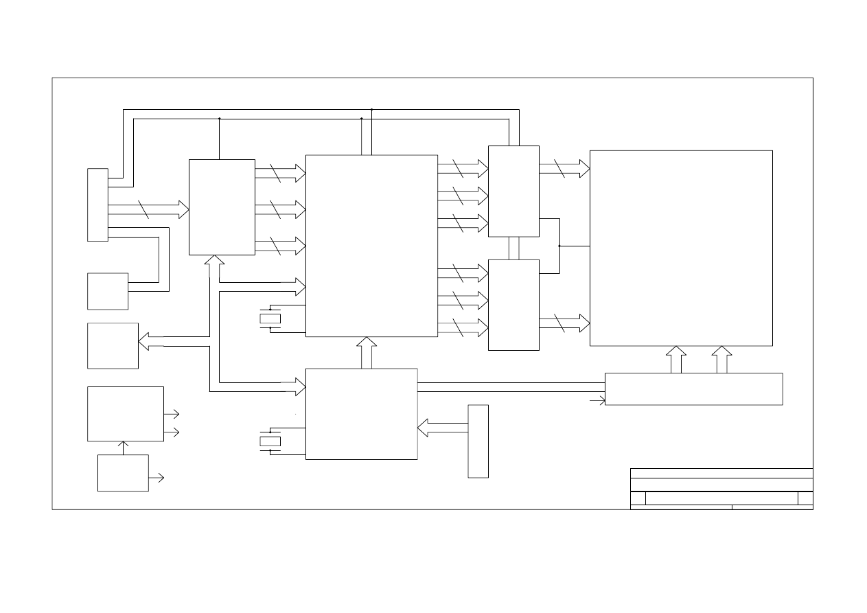
I. BLOCK DIAGRAM
ORION
B
BLOCK DIAGRAM
B
1
1
Tuesday, October 23, 2001
Title
Size
Document Number
Rev
Date:
Sheet
of
HSYNC
VSYNC
D-DE
BLK-ON/OFF
SDA
BRIGHTNESS
DDC-SCL
DDC-SDA
SCL
POWER
ADAPTER
12V
SWITCH POWER
SUPPLY AND
3V
5V
12V
C
O
N
N
E
N
T
VGA-IN
12PIN
D.D.C
24C21
EEPROM
ADC
SCALER
LVDS
LVDS
MCU
24C16
EEPROM
INVERTER
12V
C
O
N
N
E
N
T
FUNCTION KEY
8PIN
LCD PANEL(LVDS)
REGULATOR
CRYSTAL
CRYSTAL
3 {R.G.B}
12M HZ
12M HZ
8 R0~R7
8 G0~G7
8 B0~B7
8 RA0~RA7
8 GA0~GA7
8 BA0~BA7
8 RB0~RB7
8 GB0~GB7
8 BB0~BB7
10 ODD
10 EVEN
POWER
HI VOLTAGE
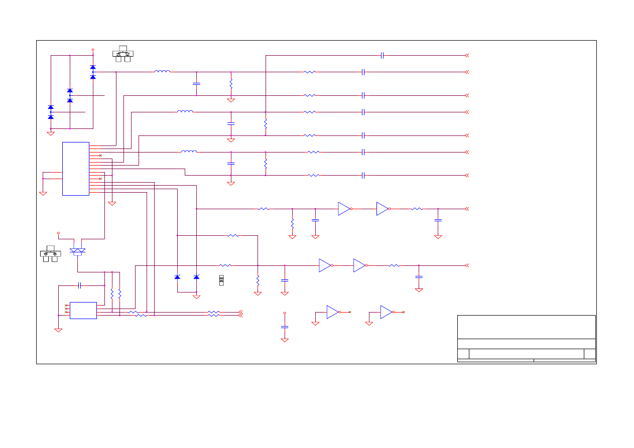
J. SCHEMATIC DIAGRAM
200-100-SH770
S4
MVP2(VGA)
Proview Electronics (Taiwan) Co., LTD.
6F, NO.1, Pau-Sheng Rd., Yung-Ho City,
Taipei County, Taiwan R.O.C.
Tel: 886-2-2231-6789 Fax: 886-2-2232-4613
1
6
Tuesday, September 10, 2002
Title
Size
Document Number
Rev
Date:
Sheet
of
VDD
VDD
VCC
RED+
2
BLUE+
2
GREEN+
2
VSYNC
2
SOG
2
RED-
2
HSYNC
2
GREEN-
2
BLUE-
2
TxD
4
RxD
4
GREEN
SDA-VGA
SCL-VGA
BLUE
VGA-VSYNC
DDC5V
VGAV5V
VGA-HSYNC
BLUE
GREEN
RED
C99
NC
U12A
74LVC14
1
2
R58
10K
CN8
VGA-15PIN-D/SHELL
1
2
3
4
5
6
7
8
9
10
11
12
13
14
15
17
16
RED
GREEN
BLUE
NC
GND
GND
GND
GND
VCC
GND
NC
MID1
HSYNC
VSYNC
MID3
GND
GND
C95
0.1uF
C64
0.1uF
C88
0.01uF
R81
75
U14
24C21
1
2
3
4
5
6
7
8
NC
NC
NC
VSS
SDA
SCK
VCLK
VCC
R49
0
R83
51
C86
0.01uF
D6
TZMC5V1(NP)
2
1
R68
0R
U12B
74LVC14
3
4
C84
0.01uF
L27
FCM1608K-300T06
L28
L28
FCM1608K-300T06
C85
NC
U12D
74LVC14
9
8
U12C
74LVC14
5
6
U12F
74LVC14
13
12
U12E
74LVC14
11
10
DN1
NP
1
3
2
DN2
NP
1
3
2
R71
0R
D7
TZMC5V1(NP)
2
1
R70
0R
D8
BAT54C-SOT23
2
3
1
R22
47
C87
0.01uF
R23
47
R69
0R
C89
0.01uF
R72
0R
C97
NC
C83
0.01uF
R67
0R
R79
75
DN3
NP
1
3
2
L26
FCM1608K-300T06
C67
22p
C66
22p
R85
47K
R61
22
R84
51
R59
10K
C98
NC
R60
22
C58
22p
R48
0
R80
75
R62
0
R77
47K
C57
22p
2
1
3
2
1
3
1
2
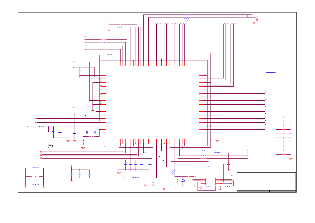
200-100-SH770
S4
MVP2(SCALER)
Proview Electronics (Taiwan) Co., LTD.
6F, NO.1, Pau-Sheng Rd., Yung-Ho City,
Taipei County, Taiwan R.O.C.
Tel: 886-2-2231-6789 Fax: 886-2-2232-4613
2
6
Tuesday, September 10, 2002
Title
Size
Document Number
Rev
Date:
Sheet
of
VDD
3.3V-PLL
3.3V-ANA
VDD
VDD
VDD
3.3DIG-PLL
3.3DIG-ANA
3.3DIG
3.3V-ANA
3.3V-REF
VDD
RESET
4
SDA
4
SCL
4
IRQ-
4
RED-
1
GREEN-
1
BLUE-
1
BLUE+
1
SOG
1
HSYNC
1
VSYNC
1
GREEN+
1
RED+
1
RGB-B[0..23]
5
RGB-A[0..23] 5
DISP-HSYNC
5
SHCLK
5
DISP-VSYNC
5
DISP-DE
5
VBLCTRL
6
VDDCTRL
5
LVDS-PD
5
PWM1_A
3
BRIGHTNESS
6
MCU_CLK
4
PWM0
DVI-CLKOUT
LCD_VDD
LCD_VBL
MCU_CLKO
GND
VDD
Vref
RGB-A2
RGB-A5
SHC
STH8
PWM1
LCD_VEE
RGB-A12
RGB-A15
RGB-A3
RGB-A10
RGB-A6
RGB-A7
RGB-A9
RGB-A0
RGB-A13
RGB-A1
RGB-A23
RGB-A14
RGB-A8
RGB-A4
RGB-A11
RGB-A22
RGB-A21
RGB-A20
RGB-A19
RGB-A18
RGB-A17
RGB-A16
RGB-B22
RGB-B20
RGB-B19
RGB-B18
RGB-B17
RGB-B5
RGB-B7
RGB-B21
RGB-B23
RGB-B16
RGB-B6
RGB-B3
RGB-B2
RGB-B1
RGB-B0
RGB-B15
RGB-B14
RGB-B13
RGB-B12
RGB-B11
RGB-B10
RGB-B9
RGB-B8
RGB-B4
MCU_CLK
MCU_CLKO
MCU_CLK
MOUT
R98 NC
C69
4.7n
T1
R100 0R
T2
C61
0.1uF
T3
T4
U9
Mascot VP-II
1
2
3
4
5
6
7
8
9
10
11
12
13
14
15
17
18
19
20
21
22
23
24
25
26
27
28
29
30
31
32
33
34
35
36
37
38
39
40
41
42
43
44
45
46
47
48
49
50
51
52
53
54
55
56
57
58
59
60
61
62
63
64
65
66
67
68
69
70
71
72
73
74
75
76
77
78
79
80
120
119
118
117
116
115
114
113
112
111
110
109
108
107
106
105
104
103
102
101
100
99
98
97
96
95
94
93
92
91
90
89
88
87
86
85
84
83
82
81
160
159
158
157
156
155
154
153
152
151
150
149
148
147
146
145
144
143
142
141
140
139
138
137
136
135
134
133
132
131
130
129
128
127
126
125
124
123
122
121
16
AGNDP
AVDDP
AVDDC
RXCN
RXCP
AGNDC
AVDD0
RX0N
RX0P
AGND0
GND0
VDD0
AVDD1
RX1N
RX1P
GND1
VDD1
AVDD2
RX2N
RX2P
AGND2
GND2
VDD2
DGND
DGND
DVDD
DVDD
DVSS
DTEST
VGA_VSYNC
VGA_HSYNC
VCCD
DGND
SOGIN
VCCA
AGND
VREF
CP
CZ
VCCAB
Reserved
BIN+
BIN-
GNDAB
BCLP
VTOP
VBOT
VCCAG
Reserved
GIN+
GIN-
GNDAG
GCLP
TOUTP
TOUTM
VCCAR
Reserved
RI+
RI-
GNDAR
RCLP
ADVDD
ADVSS
GPIO2/<OSD_FSW>
GPIO1/<OSD_CLK>
GPIO0/<OSD_R>
STH1/<OSD_G>
STH8/<OSD_B>
LP/<OSD_I>
DCVDD
SHC/<RESERVED>
XTAL
XTALI
DIBVSS
RLS/<DISP_DE>
POL/<DISP_VSYNC>
CPH1/<SHCLK>
INV1/<DISP_HSYNC>
DCVSS
DOBVSS
BLU_OUTB_7
BLU_OUTB_6
BLU_OUTB_5
BLU_OUTB_4
DOBVDD
BLU_OUTB_3
BLU_OUTB_2
BLU_OUTB_1
BLU_OUTB_0
DOBVSS
RED_OUTA_7
RED_OUTA_6
RED_OUTA_5
RED_OUTA_4
DCVDD
RED_OUTA_3
RED_OUTA_2
RED_OUTA_1
RED_OUTA_0
DCVSS
GRN_OUTA_7
GRN_OUTA_6
GRN_OUTA_5
GRN_OUTA_4
DOBVDD
GRN_OUTA_3
GRN_OUTA_2
GRN_OUTA_1
GRN_OUTA_0
DOBVSS
BLU_OUTA_7
BLU_OUTA_6
BLU_OUTA_5
BLU_OUTA_4
DOBVDD
BLU_OUTA_3
BLU_OUTA_2
BLU_OUTA_1
BLU_OUTA_0
CLKOUT
IRQ#
SCS#
SDA
SCL
RST
STV3/<GPIO1>
STV1/<GBIO0>
DCVSS
CPV
OE3/<CONFIG3>
OE2/<CONFIG2>
OE1
CPH2
PWM0
PWM1
DCVDD
INV2/<LCD_VEE>
LCD_VDD
LCD_VBL
DCVSS
RED_OUTB_7
RED_OUTB_6
RED_OUTB_5
RED_OUTB_4
DOBVDD
RED_OUTB_3
RED_OUTB_2
RED_OUTB_1
RED_OUTB_0
DOBVSS
GRN_OUTB_7
GRN_OUTB_6
GRN_OUTB_5
GRN_OUTB_4
DOBVDD
GRN_OUTB_3
GRN_OUTB_2
GRN_OUTB_1
GRN_OUTB_0
AGND1
R52
22
L17
<>
R50
22
R51
22
T8
T9
T7
C59
22p
C72
0.1uF
C74
0.1uF
L16
L0805/0R
L29
L0805/0R
R42
4.7K
R86
NC
L18
L0603
Y2
24MHZ
R57
1M
C78
22p
R43
NC
L21
L0805/0R
C82
0.1uF
R63
180
R40
10K
T5
CP1
150pF
T6
CZ1
39nF
R41
4.7K
TC25
10uF/16V
R44
22
R45
22
R99
NC
C48
330pF
C54
0.1uF
TC18
10uF/16V
C60
0.1uF
C42
0.1uF
C43
0.1uF
C41
0.1uF
C49
0.1uF
C62
0.1uF
R33
10K
C55
0.1uF
C77
0.1uF
R39
1K
C76
0.1uF
TD3
TL431
2
3
1
C56
0.1uF
R31
150
R32
150
C79
22p
C68
0.1uF
L30
L0805/0R
C70
0.01uF
C71
0.01uF
C73
4.7n
R96
NC
R97
NC
C75
4.7n
U16
P2008A
1
2
3
4
8
7
6
5
XIN
XOUT
MRA
VSS
VDD
SR0
MOUT
SSON
R
C
A
3 2 1
R96-R102
U16
200-100-SH770
S4
MVP2(AUDIO)
Proview Electronics (Taiwan) Co., LTD.
6F, NO.1, Pau-Sheng Rd., Yung-Ho City,
Taipei County, Taiwan R.O.C.
Tel: 886-2-2231-6789 Fax: 886-2-2232-4613
3
6
Tuesday, September 10, 2002
Title
Size
Document Number
Rev
Date:
Sheet
of
VCC
VCC
VCC
OPVCC
GND
GND
GND
AUD_OFF
4
PWM1_A
2
VCC_AU
Right_Outp
Left_outp
Left_Outm
LEFTIN
Left_Outm
Left_outp
Right_outm
R_P
Right_Outp
AUD4835_SD
AUD4835_DCVOL
RIGHTIN
Right_outm
L_M
L_P
R_M
C110
0.1uF
C111
0.1uF
C37
1uF
CN9
SCP606
C80
0.1uF
R87
20K
R38
2.2K
L32
L0603
R35
2.2K
R78
1K
R88
20K
R64
10K(NP)
CN5
BASE2S
1
2
R91
33K
R82
20K
U15
APA4835A
1
8
14
20
23
6
16
27
2
3
4
5
7
9
10
11
12
13
28
26
25
24
22
21
19
18
17
15
29
GND
GND
GND
GND
GND
VDD
VDD
VDD
Shutdown
Gain Select
Mode
Mute
DC_Vol
Right Dock
Right In
Beep In
Lift In
Left Dock
Right Out+
Right Out-
Right Gain2
Right Gain1
Bypass
HP Sense
Lift Gain1
Lift Gain2
Lift out -
Lift out +
GND
C103
33PF
CN10
SCP606
C105 0.33uF
R75
0(NP)
C106
0.33uF
R65
20K
C100
0.1uF
R66
33K
R76
20K
C102
0.0068UF
R90
20K
C90
0.1uF
R37
1K
R92
20K
R93
20K
C92
0.1uF
C93
0.0068UF
TC21
10uF/16V
1
2
+
-
U7A
LM358-SO8
3
2
1
8
4
R73
10K
R74
0R
+
TC7
100uF/16V
TC22
2.2UF/16V
1
2
L24 L0603
L31
L0603
L25 L0603
CN6
BASE2S
1
2
C94
33PF
L22
L0805/0R
1
2
C81
0.1uF
GAIN
HI HP OUT
SDWN
MODE
1
0
MODE VCC OP VOL
HI SHUTDOWN
MUTE
0
0
MODE GND OP MAX
1
HPS
LOW SP OUT
L-OUT
R-OUT
WHITE---L
RED----R
DEL C109 , C108, C81,C80
DEL R89,R86
DEL C107
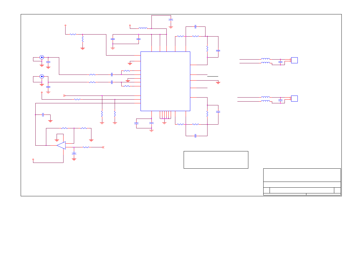
200-100-SH770
S4
MVP2(MCU)
Proview Electronics (Taiwan) Co., LTD.
6F, NO.1, Pau-Sheng Rd., Yung-Ho City,
Taipei County, Taiwan R.O.C.
Tel: 886-2-2231-6789 Fax: 886-2-2232-4613
4
6
Tuesday, September 10, 2002
Title
Size
Document Number
Rev
Date:
Sheet
of
VCC
VCC-MCU
VCC
VCC-MCU
VCC
VCC
VCC
VCC
VCC
VCC
VCC
VCC
VCC
IRQ-
2
SDA
2
RESET
2
SCL
2
TxD
1
RxD
1
AUD_OFF
3
MCU_CLK
2
RESET
MCU-LEDO
MCU-LEDG
LED_G
LED_G
OSD_POWER
SCL
MCU-LEDO
OSD_MENU
OSD_SW_LEFT
OSD_SW_RIGHT
OSD_AUTO
MCU-LEDG
ROT_PB6
ROT_LF
ROT_PB0
RESET
ROT_PB6
SW LEFT
AUTO
OSD_AUTO
OSD_SW_RIGHT
LED_G
ROT_LF
OSD_SW_LEFT
POWER
ROT_PB0
OSD_MENU
OSD_POWER
LED_O
TxD
RxD
SW_RIGHT
MENU
LED_O
LED_O
SDA
RxD
SCL
TxD
SDA
C20
0.1uF
R21
10K(NP)
P1
W78E62B-PLCC44
1
2
3
4
5
6
7
8
9
10
11
12
13
14
15
16
17
18
19
20
21
22
23
24
25
26
27
28
29
30
31
32
33
34
35
36
37
38
39
40
41
42
43
44
R6
330
L1
L0805
TC4
10uF/16V(NP)
Q1
2N3904
3
1
2
C2
22p
R9
1K
R12
1M
R4
10K
R3
10K
TU1
RESET-V6300L
3
2
1
GND
RESET
VCC
C5
0.1uF
D1
4148(NP)
1
2
C4
22p
TC1
10uF/16V
Y1
11.059MHz-49S
C12
0.1uF
R13
10K(NP)
C18
0.1uF
R8
10K
D2
LED(NP)
2
1
U2
PLCC44-SOCKET
35
21
20
10
14
15
16
17
2
3
4
5
6
7
8
9
43
42
41
40
39
38
37
36
24
25
26
27
28
29
30
31
19
18
32
33
13
11
44
22
23
34
1
12
EA/VP
X1
X2
RESET
INT0 / P3.2
INT1 / P3.3
T0 / P3.4
T1 / P3.5
P1.0 / T2
P1.1 / T2EX
P1.2
P1.3
P1.4
P1.5
P1.6
P1.7
AD0 / P0.0
AD1 / P0.1
AD2 / P0.2
AD3 / P0.3
AD4 / P0.4
AD5 / P0.5
AD6 / P0.6
AD7 / P0.7
A8 / P2.0
A9 / P2.1
A10 / P2.2
A11 / P2.3
A12 / P2.4
A13 / P2.5
A14 / P2.6
A15 / P2.7
P3.7/ RD
P3.6 / WR
PSEN
ALE
P3.1 / TXD
P3.0 / RXD
VCC
VSS
P4.0
P4.1
INT3 / P4.2
INT2 / P4.3
R24
33
C13
0.1uF
C15
22p
C28
0.1uF
RP1
33X4
1
8
2
7
3
6
4
5
C19
0.1uF
R1
33
R26
330
R7
330
C1
0.1uF
R5
NC
U6
MCP-810(NP)
3
2
1
VCC
RESET
GND
RP2
33X4(NP)
1
8
2
7
3
6
4
5
C14
22p
Q2
2N3904
3
1
2
U1
24C16B-SO8
1
2
3
4
5
6
7
8
A0
A1
A2
VSS
SDA
SCL
WP
VCC
RP4
33X4
1
8
2
7
3
6
4
5
RP3
10KX4
1
8
2
7
3
6
4
5
C3
0.1uF
R2
33
R10
1K
C11
0.1uF
C10
0.1uF
R101 100/NP
CN3
JWT-A2001WV2-06
1
2
3
4
5
6
1
2
3
4
5
6
R14
NC
R94
4.7K
R95
4.7K
CN2
WAFE-8PIN-1.5MM-90@
1
2
3
4
5
6
7
8
R102
NP
V
R
G
C
E
B
1
2
3
G
V
R
1
3
2
1
2
B
E
C
3
MCP-810
1
90@
8
PROVIEW FOR LCD COLOR ANALYZER (CHROMA 7120)
TO VGA CABLE
Update : 2002-03-09
PROVIEW KEY PAD --OK
4.DOWN-
1.Power
3.LED G
2.LED O
5.UP
6.MENU
7.AUTO
8.GND
200-100-SH770
S4
MVP2(OUTPUT)
Proview Electronics (Taiwan) Co., LTD.
6F, NO.1, Pau-Sheng Rd., Yung-Ho City,
Taipei County, Taiwan R.O.C.
Tel: 886-2-2231-6789 Fax: 886-2-2232-4613
5
6
Tuesday, September 10, 2002
Title
Size
Document Number
Rev
Date:
Sheet
of
VDD
VDD
VDD
VDD
VDD
VDD
LCDVDD
LCDVDD
VCC
RGB-B[0..23]
2
RGB-A[0..23]
2
DISP-DE
2
SHCLK
2
DISP-VSYNC
2
DISP-HSYNC
2
VDDCTRL
2
LVDS-PD
2
LVDS-PD
2
RGB-B16
RGB-B11
RGB-B3
RGB-B20
RGB-B19
RGB-B7
RGB-B17
RGB-B5
RGB-B9
RGB-B12
RGB-B18
RGB-B21
RGB-B10
RGB-B0
RGB-B1
RGB-B15
RGB-B2
RGB-B13
RGB-B4
RGB-B22
RGB-B14
RGB-B23
RGB-B8
RGB-B6
D-VSYNC
D-SHCLK2
D-HSYNC
D-DE2
GA6
GA2
GA1
GA4
GA5
GA7
GA0
GA3
GB0
GB4
GB3
GB2
GB5
GB7
GB1
GB6
D-DE2
RA1
RB2
BB0
D-SHCLK2
RB6
RA5
BA1
RA7
RA2
RB5
BA7
BB4
GB5
GA5
GA0
RA0
BB7
GA4
GB3
D-VSYNC
RA4
GA7
BB6
D-DE2
RB7
RA3
D-HSYNC
BA4
RA6
D-HSYNC
GB2
RB3
GA6
BB3
BB2
RB1
BA0
GB0
RB4
GB4
RB0
BA3
D-SHCLK2
BB1
BB5
GA2
GB7
GA3
GB1
D-VSYNC
BA5
BA2
BA6
GA1
GB6
RXO0-
RXO0+
RXO1-
RXO1+
RXE0+
RXE0-
RXE1-
RXE1+
RXO2-
RXO2+
RXOC+
RXOC-
RXO3-
RXO3+
RXE3-
RXE2+
RXE2-
RXEC-
RXE3+
RXEC+
RGB-A9
RGB-A14
RGB-A6
RGB-A4
RGB-A21
RGB-A20
RGB-A10
RGB-A1
RGB-A19
RGB-A18
RGB-A13
RGB-A16
RGB-A22
RGB-A23
RGB-A11
RGB-A7
RGB-A17
RGB-A3
RGB-A2
RGB-A8
RGB-A5
RGB-A12
RGB-A15
RGB-A0
BB5
BB2
BB4
BB6
BB0
BB1
BB3
BB7
RB5
RB0
RB1
RB7
RB3
RB6
RB4
RB2
BA4
BA1
BA0
BA5
BA2
BA7
BA6
BA3
RA4
RA3
RA5
RA6
RA2
RA1
RA0
RA7
GND
RXO0-
RXE0-
RXO3-
RXOC-
RXE0+
RXEC+
GND
RXE1+
RXO1-
RXE2-
RXE1-
RXO0+
RXO2-
GND
RXO1+
RXO2+
GND
RXOC+
RXE3-
RXO3+
RXE2+
RXEC-
RXE3+
LCDVDD-A
R15
0
U5
Si9435-SO8
4
6
3
7
2
1
8
5
L2
L0603
C24
0.1uF
C27
0.1uF
C26
0.01uF
C40
NC
U3
DS90C383-QSOP56
1
2
3
4
5
6
7
8
9
10
11
12
13
14
15
16
17
18
19
20
21
22
23
24
25
26
27
28
29
30
31
32
33
34
35
36
37
38
39
40
41
42
43
44
45
46
47
48
49
50
51
52
53
54
55
56
VCC
TXIN5
TXIN6
TXIN7
GND
TXIN8
TXIN9
TXIN10
VCC
TXIN11
TXIN12
TXIN13
GND
TXIN14
TXIN15
TXIN16
R_FB
TXIN17
TXIN18
TXIN19
GND
TXIN20
TXIN21
TXIN22
TXIN23
VCC
TXIN24
TXIN25
GND
TXIN26
TXCLKIN
PWR DWN
PLL GND
PLL VCC
PLL GND
LVDS GND
TX OUT3+
TX OUT3-
TXCLKOUT+
TXCLKOUT-
TXOUT2+
TXOUT2-
LVDS GND
LVDS VCC
TXOUT1+
TXOUT1-
TXOUT0+
TXOUT0-
LVDS GND
TXIN27
TXIN0
TXIN1
GND
TXIN2
TXIN3
TXIN4
L3
L0603
RP10 33X4
1
8
2
7
3
6
4
5
R11
10K
C21
0.1uF
L6
L0603
C36
NC
RP6
33X4
1
8
2
7
3
6
4
5
R34
33
Q3
2N3904
3
1
2
U4
DS90C383-QSOP56
1
2
3
4
5
6
7
8
9
10
11
12
13
14
15
16
17
18
19
20
21
22
23
24
25
26
27
28
29
30
31
32
33
34
35
36
37
38
39
40
41
42
43
44
45
46
47
48
49
50
51
52
53
54
55
56
VCC
TXIN5
TXIN6
TXIN7
GND
TXIN8
TXIN9
TXIN10
VCC
TXIN11
TXIN12
TXIN13
GND
TXIN14
TXIN15
TXIN16
R_FB
TXIN17
TXIN18
TXIN19
GND
TXIN20
TXIN21
TXIN22
TXIN23
VCC
TXIN24
TXIN25
GND
TXIN26
TXCLKIN
PWR DWN
PLL GND
PLL VCC
PLL GND
LVDS GND
TX OUT3+
TX OUT3-
TXCLKOUT+
TXCLKOUT-
TXOUT2+
TXOUT2-
LVDS GND
LVDS VCC
TXOUT1+
TXOUT1-
TXOUT0+
TXOUT0-
LVDS GND
TXIN27
TXIN0
TXIN1
GND
TXIN2
TXIN3
TXIN4
RP12 33X4
1
8
2
7
3
6
4
5
RP8
33X4
1
8
2
7
3
6
4
5
C38
NC
RP5
33X4
1
8
2
7
3
6
4
5
C17
0.1uF
C25
0.1uF
C44
NC
C23
0.1uF
C6
0.1uF
RP13 33X4
1
8
2
7
3
6
4
5
C22
0.1uF
L4
L0603
CN1
JSTB30B-PHDSS
1
2
3
4
5
6
7
8
9
10
11
12
13
14
15
16
17
18
19
20
21
22
23
24
25
26
27
28
29
30
C16
0.1uF
L1209
L8
L7
L0603
RP14 33X4
1
8
2
7
3
6
4
5
C39
NC
RP7
33X4
1
8
2
7
3
6
4
5
C45
NC
RP9
33X4
1
8
2
7
3
6
4
5
R17
4.7K
C8
0.1uF
C9
0.1uF
RP11 33X4
1
8
2
7
3
6
4
5
R18
4.7K(NP)
RP15 33X4
1
8
2
7
3
6
4
5
C35
NC
RP16 33X4
1
8
2
7
3
6
4
5
TC3
220uF/16V
R16
0
R30
33
C34
NC
L5
L0603
R36
33
C31
0.1uF
TD1
ICBE-TO92/NC
2
3
1
G
O
I
C7
0.1uF
R19
4.7K(NP)
TC2
220uF/16V
R46
33
R203
RA
GA
BA
GB
BB
RB
BA-->>RA
RA-->>BA
BB-->>RB
RB-->>BB
A PORT TO CMO M170E1 first pixel EVEN
A PORT TO CMO M170E4 first pixel ODD
1
30
SH770" PC+AUDIO
3-17
6-14
20-23
21-22
5-15
16-26
15-27
10-11
23-20
2-18
9-12
13-28
18-25
11-10
8-13
4-16
12-29
19-24
22-21
1-19
E
C
2
DEFAULT = 0
3
B
1
9/10修改
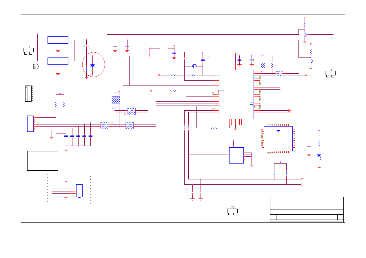
200-100-SH770
S4
MVP2(POWER)
Proview Electronics (Taiwan) Co., LTD.
6F, NO.1, Pau-Sheng Rd., Yung-Ho City,
Taipei County, Taiwan R.O.C.
Tel: 886-2-2231-6789 Fax: 886-2-2232-4613
6
6
Tuesday, September 10, 2002
Title
Size
Document Number
Rev
Date:
Sheet
of
VCC
3.3V-PLL
3.3V-ANA
VCC
12VA
3.3V
VDD
3.3DIG-ANA
3.3DIG-PLL
3.3DIG
GND_EARTH
12VIN
VCC
OPVCC
VDD
12VA
12VA
GND_EARTH
GND
GND_EARTH
GND
GND
12VA
3.3V-REF
BRIGHTNESS
2
VBLCTRL
2
3.3V
VBLCTRL
VBR
12VIN
VCCA
VCC-ST
R202
10K
TR1
WR-C-5W0.02-1/4W
R27
0
L9
L1206
C46
0.1uF
D4
SB340
2
1
R29
4.7K
TC5
10uF/16V
C104
0.1uF
C96
0.1uF
C91
0.1uF
W4
TP
1
1
W5
TP
1
1
L1206
L14
TC12
10uF/16V
U10
Si9435-SO8
1
2
3
4
8
7
6
5
S1
S2
S3
G
D4
D3
D2
D1
U11
AIC1578-SO8
1
2
3
4
8
7
6
5
VIN
DUTY
SHDN
FB
CS+
CS-
DRI
GND
C65
0.1uF
+
-
U7B
LM358-SO8
5
6
7
8
4
L15
L0805
D3
D3235(NP)
2
1
L23
L0603
C51
0.1uF
TC30
EMI_GND
1
2
3
4
5
6
7
8
C30
0.1uF
C63
330pF
TL2
JBT0385-100805-4
R56
2K_1%
R53
6.2K_1%
TC14
47uF/16V
L0805/0R
L11
L0805/0R
L13
TC29
EMI_GND
1
2
3
4
5
6
7
8
TC34
EMI_GND
1
2
3
4
5
6
7
8
C32
1uF
TC36
EMI_GND
1
2
3
4
5
6
7
8
R28
1K
R20
2.2K
TC37
EMI_GND
1
2
3
4
5
6
7
8
TC11
10uF/16V
TR2
JUMP WIRE_2
+
TC19
220uF/16V
W6
GND
1
2
3
4
5
6
7
8
9
+
TC13
220uF/16V
TD2
1N5822(NP)
2
1
C53
0.1uF
TC28
EMI_GND
1
2
3
4
5
6
7
8
TL1
33uH@3ADIP
TC35
EMI_GND
1
2
3
4
5
6
7
8
TC27
EMI_GND
1
2
3
4
5
6
7
8
R54
10K
TC31
EMI_GND
1
2
3
4
5
6
7
8
L10
L0805
TC33
EMI_GND
1
2
3
4
5
6
7
8
R55
20K(NP)
TC32
EMI_GND
1
2
3
4
5
6
7
8
L12
L0805
TC6
220uF/16V
TC10
100uF/16V
L20
L0805
L19
L0805
+
TC20
220uF/16V
U8
LT1084
1
2
3
4
ADJ
VOUT
VIN
VOUT1
C29
1uF
C101
0.1uF
W2
GND
1
2
3
4
5
6
7
8
9
F1
FUS1206-5A
TC16
10uF/16V
TC15
10uF/16V
W7
GND
1
2
3
4
5
6
7
8
9
R25
0
W1
GND
1
2
3
4
5
6
7
8
9
C52
0.1uF
CN7
DC-JACK
5
4
3
2
1
C50
0.1uF
U13
LT1117CST-3.3
1
2
3
4
ADJ
VOUT
VIN
VOUT1
TC23
47uF/16V
TC24
10uF/16V
CN4
JST-2.0-6PIN
1
2
3
4
5
6
R201
10K
+
TC26
220uF/16V
TC17
22uF/16V
C33
0.1uF
W3
TP
1
1
S2
COPPER2
2
1
D5
D3235(NP)
2
1
R47
0(0805)
S1
COPPER2
2
1
C47
0.1uF
+
TC9
220uF/16V
+
TC8
10uF/16V
N12829335
3.3V
G
1
I
3
O
2
O
4
I
G
3
AME810&AIC1117
1
2
O
9/10修改

Memu
Wyszukiwarka
Podobne podstrony:
więcej podobnych podstron