
LETTERS
Detection of individual gas molecules
adsorbed on graphene
F. SCHEDIN
1
, A. K. GEIM
1
, S. V. MOROZOV
2
, E. W. HILL
1
, P. BLAKE
1
, M. I. KATSNELSON
3
AND K. S. NOVOSELOV
1
*
1
Manchester Centre for Mesoscience and Nanotechnology, University of Manchester, Manchester, M13 9PL, UK
2
Institute for Microelectronics Technology, 142432 Chernogolovka, Russia
3
Institute for Molecules and Materials, University of Nijmegen, 6525 ED Nijmegen, Netherlands
*
e-mail: Konstantin.Novoselov@manchester.ac.uk
Published online: 29 July 2007; doi:10.1038/nmat1967
The ultimate aim of any detection method is to achieve such
a level of sensitivity that individual quanta of a measured
entity can be resolved. In the case of chemical sensors, the
quantum is one atom or molecule. Such resolution has so far
been beyond the reach of any detection technique, including
solid-state gas sensors hailed for their exceptional sensitivity
.
The fundamental reason limiting the resolution of such sensors
is fluctuations due to thermal motion of charges and defects
,
which lead to intrinsic noise exceeding the sought-after signal
from individual molecules, usually by many orders of magnitude.
Here, we show that micrometre-size sensors made from graphene
are capable of detecting individual events when a gas molecule
attaches to or detaches from graphene’s surface. The adsorbed
molecules change the local carrier concentration in graphene one
by one electron, which leads to step-like changes in resistance.
The achieved sensitivity is due to the fact that graphene is an
exceptionally low-noise material electronically, which makes it
a promising candidate not only for chemical detectors but also
for other applications where local probes sensitive to external
charge, magnetic field or mechanical strain are required.
Solid-state gas sensors are renowned for their high sensitivity,
which—in combination with low production costs and miniature
sizes—have made them ubiquitous and widely used in many
applications
. Recently, a new generation of gas sensors has
been demonstrated using carbon nanotubes and semiconductor
nanowires (see, for example, refs 3,4). The high acclaim received
by the latter materials is, to a large extent, due to their exceptional
sensitivity allowing detection of toxic gases in concentrations
as small as 1 part per billion (p.p.b.). This and even higher
levels of sensitivity are sought for industrial, environmental and
military monitoring.
The operational principle of graphene devices described below
is based on changes in their electrical conductivity,
σ
, due to gas
molecules adsorbed on graphene’s surface and acting as donors
or acceptors, similar to other solid-state sensors
. However, the
following characteristics of graphene make it possible to increase
the sensitivity to its ultimate limit and detect individual dopants.
First, graphene is a strictly two-dimensional material and, as
such, has its whole volume exposed to surface adsorbates, which
maximizes their effect. Second, graphene is highly conductive,
exhibiting metallic conductivity and, hence, low Johnson noise even
in the limit of no charge carriers
, where a few extra electrons
can cause notable relative changes in carrier concentration,
n
.
Third, graphene has few crystal defects
, which ensures a low
level of excess
(
1
/f )
noise caused by their thermal switching
.
Fourth, graphene allows four-probe measurements on a single-
crystal device with electrical contacts that are ohmic and have
low resistance. All of these features contribute to make a unique
combination that maximizes the signal-to-noise ratio to a level
sufficient for detecting changes in a local concentration by less than
one electron charge,
e
, at room temperature.
The
studied
graphene
devices
were
prepared
by
micromechanical cleavage of graphite at the surface of oxidized
Si wafers
. This allowed us to obtain graphene monocrystals of
typically 10
µ
m in size. By using electron-beam lithography, we
made electrical (Au/Ti) contacts to graphene and then defined
multiterminal Hall bars by etching graphene in an oxygen
plasma. The microfabricated devices (Fig. 1a, upper inset) were
placed in a variable temperature insert inside a superconducting
magnet and characterized by using field-effect measurements
at temperatures,
T
, from 4 to 400 K and in magnetic fields,
B
,
up to 12 T. This allowed us to find the mobility,
µ
, of charge
carriers (typically,
≈
5,000 cm
2
V
−
1
s
−
1
) and distinguish between
single-, bi- and few-layer devices, in addition to complementary
measurements of their thickness carried out by optical and atomic
force microscopy
. Figure 1a, lower inset, shows an example
of the field-effect behaviour exhibited by our devices at room
temperature. This plot shows that longitudinal (
ρ
xx
) and Hall
(
ρ
xy
) resistivities are symmetric and antisymmetric functions
of gate voltage,
V
g
, respectively.
ρ
xx
exhibits a peak at zero
V
g
,
whereas
ρ
xy
simultaneously passes through zero, which shows that
the transition from electron to hole transport occurs at zero
V
g
indicating that graphene is in its pristine undoped state
.
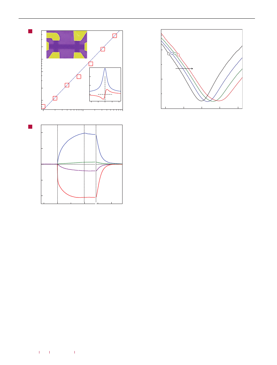
To assess the effect of gaseous chemicals on graphene devices,
the insert was evacuated and then connected to a relatively large
(5 l) glass volume containing a selected chemical strongly diluted
in pure helium or nitrogen at atmospheric pressure. Figure 1b
shows the response of zero-field resistivity,
ρ = ρ
xx
(B =
0
) =
1
/σ
,
to NO
2
, NH
3
, H
2
O and CO in concentrations,
C
, of 1 part per
million (p.p.m.). Large easily detectable changes that occurred
within 1 min and, for the case of NO
2
, practically immediately after
letting the chemicals in can be seen. The initial rapid response
was followed by a region of saturation, in which the resistivity
changed relatively slowly. We attribute this region to redistribution
652
nature
materials
VOL 6 SEPTEMBER 2007 www.nature.com/naturematerials
©
2007
Nature Publishing Group
LETTERS
0.1
1
C (p.p.m.)
Δ
n
(10
10
cm
–2
)
10
1
2
5
10
20
50
–20
0
V
g
(V)
0
2
4
20
and
xy
(k
Ω
)
ρ
ρ
ρ
ρρ
ρ
~ ~
0
500
1,000
–4
–2
0
2
4
t (s)
Δ
/
(%)
I
II
III
IV
NH
3
CO
H
2
O
NO
2
a
b
xy
Figure 1
Sensitivity of graphene to chemical doping. a, Concentration,
1n, of
chemically induced charge carriers in single-layer graphene exposed to different
concentrations, C, of NO
2
. Upper inset: Scanning electron micrograph of this device
(in false colours matching those seen in visible optics). The scale of the micrograph
is given by the width of the Hall bar, which is 1 µm. Lower inset: Characterization of
the graphene device by using the electric-field effect. By applying positive (negative)
V
g
between the Si wafer and graphene, we induced electrons (holes) in graphene in
concentrations n =
αV
g
. The coefficient
α ≈ 7.2×10
10
cm
−
2
V
−
1
was found from
Hall-effect measurements
. To measure Hall resistivity,
ρ
xy
, B = 1 T was applied
perpendicular to graphene’s surface. b, Changes in resistivity,
ρ, at zero B caused
by graphene’s exposure to various gases diluted in concentration to 1 p.p.m. The
positive (negative) sign of changes is chosen here to indicate electron (hole) doping.
Region I: the device is in vacuum before its exposure; II: exposure to a 5 l volume of
a diluted chemical; III: evacuation of the experimental set-up; and IV: annealing at
150
◦
C. The response time was limited by our gas-handling system and a
several-second delay in our lock-in-based measurements. Note that the annealing
caused an initial spike-like response in
ρ, which lasted for a few minutes and was
generally irreproducible. For clarity, this transient region between III and IV
is omitted.
of adsorbed gas molecules between different surfaces in the insert.
After a near-equilibrium state was reached, we evacuated the
container again, which led only to small and slow changes in
ρ
(region III in Fig. 1b), indicating that adsorbed molecules were
–40
–20
0
20
40
0
1
2
V
g
(V)
σ
(k
Ω
–1
)
Figure 2
Constant mobility of charge carriers in graphene with increasing
chemical doping. Doping increased from zero (black curve) to ∼1
.5×10
12
cm
−
2
(red curve) due to increasing exposure to NO
2
. Conductivity,
σ, of single-layer
graphene away from the neutrality point changes approximately linearly with
increasing V
g
and the steepness of the
σ(V
g
) curves (away from the neutrality point)
characterizes the mobility,
µ (refs 6–9). Doping with NO
2
adds holes but also
induces charged impurities. The latter apparently do not affect the mobility of either
electrons or holes. The parallel shift implies a negligible scattering effect of the
charged impurities induced by chemical doping. The open symbols on the curves
indicate the same total concentration of holes, n
t
(∼2
.7×10
12
cm
−
2
), as found
from Hall measurements. The practically constant
σ for the same n
t
yields
that the absolute mobility,
µ = σ/n
t
e, as well as the Hall mobility are
unaffected by chemical doping. For further analysis and discussions, see the
Supplementary Information.
strongly attached to the graphene devices at room temperature.
Nevertheless, we found that the initial undoped state could be
recovered by annealing at 150
◦
C in vacuum (region IV). Repetitive
exposure–annealing cycles showed no ‘poisoning’ effects of these
chemicals (that is, the devices could be annealed back to their initial
state). A short-time ultraviolet illumination offered an alternative
to thermal annealing.
To gain further information about the observed chemical
response, we simultaneously measured changes in
ρ
xx
and
ρ
xy
caused by gas exposure, which allowed us to find directly (1)
concentrations,
1n
, of chemically induced charge carriers, (2)
their sign and (3) mobilities. The Hall measurements revealed that
NO
2
, H
2
O and iodine acted as acceptors, whereas NH
3
, CO and
ethanol were donors. We also found that, under the same exposure
conditions,
1n
depended linearly on the concentration,
C
, of an
examined chemical (see Fig. 1a). To achieve the linear conductance
response, we electrically biased our devices (by more than
±
10 V)
to higher-concentration regions, away from the neutrality point, so
that both
σ = neµ
and Hall conductivity,
σ
xy
=
1
/ρ
xy
=
ne
/B
, were
proportional to
n
. The linear response
as a function of
C
should greatly simplify the use of graphene-based
sensors in practical terms.
Chemical doping also induced impurities in graphene in
concentrations
N
i
=
1n
. However, despite these extra scatterers,
we found no notable changes in
µ
even for
N
i
exceeding
10
12
cm
−
2
. Figure 2 shows this unexpected observation by showing
the electric-field effect in a device repeatedly doped with
NO
2
. V-shaped
σ(V
g
)
curves characteristic for graphene
nature
materials
VOL 6 SEPTEMBER 2007 www.nature.com/naturematerials
653
©
2007
Nature Publishing Group
LETTERS
0
10
1e
1e
20
30
Changes in
xy
(Ω
)
t (s)
ρ
0
–4
–2
0
2
4
δ
–4
–2
0
2
4
200
400
600
0
200
400
600
R (
Ω)
δR (
Ω)
Number of steps
Number of steps
Adsorption
Desorption
Desorption events
Adsorption events
+1e
–1e
0
200
400
600
a
b
c
Figure 3
Single-molecule detection. a, Examples of changes in Hall resistivity observed near the neutrality point (|n|
< 10
11
cm
−
2
) during adsorption of strongly diluted NO
2
(blue curve) and its desorption in vacuum at 50
◦
C (red curve). The green curve is a reference—the same device thoroughly annealed and then exposed to pure He. The
curves are for a three-layer device in B = 10 T. The grid lines correspond to changes in
ρ
xy
caused by adding one electron charge, e (δR ≈ 2
.5 ), as calibrated in
independent measurements by varying V
g
. For the blue curve, the device was exposed to 1 p.p.m. of NO
2
leaking at a rate of ≈10
−
3
mbar l s
−
1
. b,c, Statistical distribution of
step heights, δR, in this device without its exposure to NO
2
(in helium) (b) and during a slow desorption of NO
2
(c). For this analysis, all changes in
ρ
xy
larger than 0
.5 and
quicker than 10 s (lock-in time constant was 1 s making the response time of ≈6 s) were recorded as individual steps. The dotted curves in textbfc are automated gaussian
fits (see the Supplementary Information).
can be seen. Their slopes away from the neutrality point provide
a measure of impurity scattering (so-called field-effect mobility,
µ = 1σ/1ne = 1σ/eα1V
g
). The chemical doping only shifted
the curves as a whole, without any significant changes in their
shape, except for the fact that the curves became broader around the
neutrality point (the latter effect is discussed in the Supplementary
Information). The parallel shift unambiguously proves that the
chemical doping did not affect scattering rates. Complementary
measurements in magnetic field showed that the Hall-effect
mobility,
µ = ρ
xy
/ρ
xx
B
, was also unaffected by the doping
and exhibited values very close to those determined from the
electric-field effect. Further analysis yields that chemically induced
ionized impurities in graphene in concentrations
>
10
12
cm
−
2
(that
is, less than 10 nm apart) should not be a limiting factor for
µ
until
it reaches values of the order of 10
5
cm
2
V
−
1
s
−
1
, which translates
into a mean free path as large as
≈
1
µ
m (see the Supplementary
Information). This is in striking contrast with conventional
two-dimensional systems, in which such high densities of charged
impurities are detrimental for ballistic transport, and also disagrees
by a factor of
>
10 with recent theoretical estimates for the
case of graphene
. Our observations clearly raise doubts about
charged impurities being the scatterers that currently limit
µ
in
graphene
. In the Supplementary Information, we show that a
few-nanometre-thick layer of absorbed water provides sufficient
dielectric screening to explain the suppressed scattering on charged
impurities. We also suggest there that microscopic corrugations of
a graphene sheet
could be dominant scatterers.
The detection limit for solid-state gas sensors is usually defined
as the minimal concentration that causes a signal exceeding
the sensors’ intrinsic noise
. In this respect, a typical noise
level in our devices,
1ρ/ρ ≈
10
−
4
(see Fig. 1b), translates into
the detection limit of the order of 1 p.p.b. This already puts
graphene on par with other materials used for most sensitive gas
sensors
. Furthermore, to demonstrate the fundamental limit
for the sensitivity of graphene-based gas sensors, we optimized
our devices and measurements as described in the Supplementary
Information. In brief, we used high driving currents to suppress the
Johnson noise, annealed devices close to the neutrality point, where
relative changes in
n
were largest for the same amount of chemical
doping, and used few-layer graphene (typically, 3–5 layers), which
allowed a contact resistance of
≈
100
, much lower than for single-
layer graphene. We also used the Hall geometry that provided the
largest response to small changes in
n
near the neutrality point
(see Fig. 1a, lower inset). In addition, this measurement geometry
minimizes the sensitive area to the central region of the Hall cross
(
≈
1
µ
m
2
in size) and allows changes in
ρ
xy
to be calibrated directly
in terms of charge transfer by comparing the chemically induced
signal with the known response to
V
g
. The latter is important for
the low-concentration region, where the response of
ρ
xy
to changes
in
n
is steepest, but there is no simple relation between
ρ
xy
and
n
.
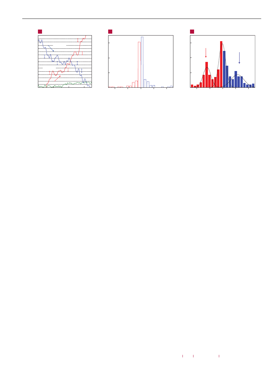
Figure 3 shows changes in
ρ
xy
caused by adsorption and
desorption of individual gas molecules. In these experiments, we
first annealed our devices close to the pristine state and then
exposed them to a small leak of strongly diluted NO
2
, which was
adjusted so that
ρ
xy
remained nearly constant over several minutes
(that is, we tuned the system close to thermal equilibrium where
the number of adsorption and desorption events within the Hall
cross area was reasonably small). In this regime, the chemically
induced changes in
ρ
xy
were no longer smooth but occurred in
a step-like manner as shown in Fig. 3a (blue curve). If we closed
the leak and started to evacuate the sample space, similar steps
occurred but predominantly in the opposite direction (red curve).
For finer control of the adsorption/desorption rates, we found it
useful to slightly adjust the temperature while keeping the same
leak rate. The characteristic size,
δ
R
, of the observed steps in
terms of ohms depended on
B
, the number of graphene layers
and, also, varied strongly from one device to another, reflecting the
fact that the steepness of the
ρ
xy
curves near the neutrality point
(see Fig. 1a, lower inset) could be different for different devices
.
However, when the steps were recalibrated in terms of equivalent
changes in
V
g
, we found that to achieve the typical value of
δ
R
it always required exactly the same voltage changes,
≈
1
.
5 mV, for
all of our 1
µ
m devices and independently of
B
. The latter value
corresponds to
1n ≈
10
8
cm
−
2
and translates into one electron
charge,
e
, removed from or added to the area of 1
×
1
µ
m
2
of
the Hall cross (note that changes in
ρ
xy
as a function of
V
g
were
smooth, that is, no charge quantization in the devices’ transport
characteristics occurred—as expected). As a reference, we repeated
654
nature
materials
VOL 6 SEPTEMBER 2007 www.nature.com/naturematerials
©
2007
Nature Publishing Group

LETTERS
the same measurements for devices annealed for 2 days at 150
◦
C
and found no or very few steps (green curve).
The curves shown in Fig. 3a clearly suggest individual
adsorption and desorption events but statistical analysis is required
to prove this. To this end, we recorded a large number of curves
such as that in Fig. 3a (
≈
100 h of continuous recording). The
resulting histograms with and without exposure to NO
2
are shown
in Fig. 3b,c (a histogram for another device is shown in the
Supplementary Information). The reference curves exhibited many
small (positive and negative) steps, which gave rise to a ‘noise
peak’ at small
δ
R
. Large steps were rare. On the contrary, slow
adsorption of NO
2
or its subsequent desorption led to many
large, single-electron steps. The steps were not equal in size,
as expected, because gas molecules could be adsorbed anywhere
including the fringes of the sensitive area, which should result in
varying contributions. Moreover, because of a finite time constant
(1 s) used in these sensitive measurements, random resistance
fluctuations could overlap with individual steps either enhancing
or reducing them and, also, different events could overlap in time
occasionally (such as the largest step on the red curve in Fig. 3a,
which has a quadruple height). The corresponding histogram
(Fig. 3c) shows the same ‘noise peak’ as the reference in Fig. 3b
but, in addition, there are two extra maxima that are centred
at a value of
δ
R
, which corresponds to removing/adding one
acceptor from the detection area. The asymmetry in the statistical
distribution in Fig. 3c corresponds to the fact that single-acceptor
steps occur predominantly in one direction, that is, NO
2
on-average
desorbs from graphene’s surface in this particular experiment. The
observed behaviour leaves no doubt that the changes in graphene
conductivity during chemical exposure were quantized, with each
event signalling adsorption or desorption of a single NO
2
molecule.
In summary, graphene-based gas sensors allow the ultimate
sensitivity such that the adsorption of individual gas molecules
could be detected. Large arrays of such sensors would increase
the catchment area
, allowing higher sensitivity for short-time
exposures and the detection of active (toxic) gases in as minute
concentrations as practically desirable. The epitaxial growth of few-
layer graphene
offers a realistic promise of mass production
of such devices. Our experiments also show that graphene is
sufficiently electronically quiet to be used in single-electron
detectors operational at room temperature
and in ultrasensitive
sensors of magnetic field or mechanical strain
, in which the
resolution is often limited by 1
/f
noise. Equally important
is the
demonstrated possibility of chemical doping of graphene by both
electrons and holes in high concentrations without deterioration of
its mobility. This should allow microfabrication of p–n junctions,
which attract significant interest from the point of view of both
fundamental physics and applications. Despite its short history,
graphene is considered to be a promising material for electronics by
both academic and industrial researchers
, and the possibility
of its chemical doping further improves the prospects of graphene-
based electronics.
Received 14 May 2007; accepted 2 July 2007; published 29 July 2007.
References
1. Moseley, P. T. Solid state gas sensors.
Meas. Sci. Technol.
8, 223–237 (1997).
2. Capone, S.
et al
. Solid state gas sensors: State of the art and future activities.
J. Optoelect. Adv. Mater.
5, 1335–1348 (2003).
3. Kong, J.
et al
. Nanotube molecular wires as chemical sensors.
Science
287, 622–625 (2000).
4. Collins, P. G., Bradley, K., Ishigami, M. & Zettl, A. Extreme oxygen sensitivity of electronic properties
of carbon nanotubes.
Science
287, 1801–1804 (2000).
5. Dutta, P. & Horn, P. M. Low-frequency fluctuations in solids: 1/f noise.
Rev. Mod. Phys.
53,
497–516 (1981).
6. Geim, A. K. & Novoselov, K. S. The rise of graphene.
Nature Mater.
6, 183–191 (2007).
7. Novoselov, K. S.
et al
. Two dimensional atomic crystals.
Proc. Natl Acad. Sci. USA
102,
10451–10453 (2005).
8. Novoselov, K. S.
et al
. Two dimensional gas of massless Dirac fermions in graphene.
Nature
438,
197–200 (2005).
9. Zhang, Y., Tan, J. W., Stormer, H. L. & Kim, P. Experimental observation of the quantum Hall effect
and Berry’s phase in graphene.
Nature
438, 201–204 (2005).
10. Dresselhaus, M. S. & Dresselhaus, G. Intercalation compounds of graphite.
Adv. Phys.
51,
1–186 (2002).
11. Ando, T. Screening effect and impurity scattering in monolayer graphene.
J. Phys. Soc. Jpn.
75,
074716 (2006).
12. Nomura, K. & MacDonald, A. H. Quantum Hall ferromagnetism in graphene.
Phys. Rev. Lett.
96,
256602 (2006).
13. Hwang, E. H., Adam, S. & Das Sarma, S. Carrier transport in two-dimensional graphene layers.
Phys.
Rev. Lett.
98, 186806 (2007).
14. Morozov, S. V.
et al
. Strong suppression of weak localization in graphene.
Phys. Rev. Lett.
97,
016801 (2006).
15. Meyer, J. C.
et al
. The structure of suspended graphene sheets.
Nature
446, 60–63 (2007).
16. Sheehan, P. E. & Whitman, L. J. Detection limits for nanoscale biosensors.
Nano Lett.
5,
803–807 (2005).
17. Berger, C.
et al
. Electronic confinement and coherence in patterned epitaxial graphene.
Science
312,
1191–1196 (2006).
18. Ohta, T., Bostwick, A., Seyller, T., Horn, K. & Rotenberg, E. Controlling the electronic structure of
bilayer graphene.
Science
313, 951–954 (2006).
19. Barbolina, I. I.
et al
. Submicron sensors of local electric field with single-electron resolution at room
temperature.
Appl. Phys. Lett.
88, 013901 (2006).
20. Bunch, J. S.
et al
. Electromechanical resonators from graphene sheets.
Science
315, 490–493 (2007).
21. Zhou, C., Kong, J., Yenilmez, E. & Dai, H. Modulated chemical doping of individual carbon
nanotubes.
Science
290, 1552–1555 (2000).
22. Obradovic, B.
et al
. Analysis of graphene nanoribbons as a channel material for field-effect
transistors.
Appl. Phys. Lett.
88, 142102 (2006).
Acknowledgements
We thank A. MacDonald, S. Das Sarma and V. Falko for illuminating discussions. This work was
supported by the EPSRC (UK) and the Royal Society. M.I.K. acknowledges financial support from
FOM (Netherlands).
Correspondence and requests for materials should be addressed to K.S.N.
Supplementary Information accompanies this paper on www.nature.com/naturematerials.
Author contributions
K.S.N. designed the experiment and carried out both experimental work and data analysis, A.K.G.
suggested the research direction and wrote the manuscript, F.S. and P.B. made graphene devices,
S.V.M. and E.W.H. helped with experiments and their analysis and M.I.K. provided theory support. All
authors participated in discussions of the research.
Competing financial interests
The authors declare no competing financial interests.
Reprints and permission information is available online at http://npg.nature.com/reprintsandpermissions/
nature
materials
VOL 6 SEPTEMBER 2007 www.nature.com/naturematerials
655
©
2007
Nature Publishing Group
Document Outline
- Detection of individual gas molecules adsorbed on graphene
- Figure 1 Sensitivity of graphene to chemical doping.
- Figure 2 Constant mobility of charge carriers in graphene with increasing chemical doping.
- Figure 3 Single-molecule detection.
- References
- Acknowledgements
- Author contributions
- Competing financial interests
Wyszukiwarka
Podobne podstrony:
30 Nature Mater 6 652 655 2007
Geim The rise of graphene Nature Mater 6 183 191 March 2007
30 31 607 pol ed01 2007
25 Appl Rev Lett 91 233108 2007 Nieznany (2)
15 Nature Nano 3 210 215 2008id Nieznany (2)
Mapy polityczne konturowe 2007 Nieznany
Mapy polityczne konturowe 2007 Nieznany (2)
AGPA Practice Guidelines 2007 P Nieznany (2)
30 03 2011 CA id 34478 Nieznany (2)
30 31 607 pol ed01 2007
30 31 307cc pol ed02 2007
34 Nature Materials 6 198 201 2007
Mikrokontrolery F Marecki id 30 Nieznany
cwwo27 word 2007 pl cwiczenia p Nieznany
PIF2 2007 Wykl 09 Dzienne id 35 Nieznany
więcej podobnych podstron