
LXT971A/972A 3.3V PHY
Transceivers Design and Layout
Guide
Application Note
November 2001
Order Number:
249016-003

2
Application Note
Document #: 249016
Revision #: 003
Rev. Date: November 1, 2001
Information in this document is provided in connection with Intel
®
products. No license, express or implied, by estoppel or otherwise, to any intellectual
property rights is granted by this document. Except as provided in Intel’s Terms and Conditions of Sale for such products, Intel assumes no liability
whatsoever, and Intel disclaims any express or implied warranty, relating to sale and/or use of Intel products including liability or warranties relating to
fitness for a particular purpose, merchantability, or infringement of any patent, copyright or other intellectual property right. Intel products are not
intended for use in medical, life saving, or life sustaining applications.
Intel may make changes to specifications and product descriptions at any time, without notice.
The LXT971A and LXT972A may contain design defects or errors known as errata which may cause the product to deviate from published
specifications. Current characterized errata are available on request.
Contact your local Intel sales office or your distributor to obtain the latest specifications and before placing your product order.
Copies of documents which have an ordering number and are referenced in this document, or other Intel literature may be obtained by calling
1-800-548-4725 or by visiting Intel’s website at http://www.intel.com.
Copyright © Intel Corporation, 2001
*Third-party brands and names are the property of their respective owners.

Application Note
3
Document #: 249016
Revision #: 003
Rev. Date: November 1, 2001
Contents
Contents
.................................................................................................. 7
.................................................................................... 8
................................................................................... 11
Avoiding Loop Antenna .......................................................................... 12
................................................................................................................ 15
................................................................................................... 16
Transmit Interface Circuit ....................................................................... 17
5.1.2.1 Common-Mode Choke .............................................................. 17
5.1.2.2 Meeting IEEE Requirements ..................................................... 19
Bob Smith Termination........................................................................... 20
LXT971A Design and Layout Checklist
........................................................... 25

4
Application Note
Document #: 249016
Revision #: 003
Rev. Date: November 1, 2001
Contents
Figures
Internal Routing of Analog and Digital Power Signals......................................... 13
Tables
Application Note
5
Document #: 249016
Revision #: 003
Rev. Date: November 1, 2001
Contents
Revision History
Date
Revision
Page
Description
November 1, 2001
003
Added last bullet.
Added Appendix A: LXT971A Design and Layout Checklist
January 2001
002
Added new language for system clock requirements.
Change “6 mm” to “6 mils” and “8 mm” to “8 mils”.
Add crystal/crystal oscillator table.


LXT971A/972A 3.3V PHY Transceivers Design and Layout Guide
Application Note
7
Document #: 249016
Revision #: 003
Rev. Date: November 1, 2001
1.0
General Description
This application note provides detailed design and layout guidelines for achieving optimum
performance using Intel’s LXT971A or LXT972A 3.3V Dual-Speed PHY Transceiver. Adherence
to these guidelines helps ensure a successful design that meets IEEE requirements.
Note:
This application note uses the singular designation “LXT971A” to refer to both the LXT971A and
LXT972A devices, unless otherwise specified.
This document also supports the LXT971 and LXT972 devices.
The following topics are discussed in this document:
Design Guidelines: Good design practices prevent most common signal and noise issues. General
guidelines listed in this section should be followed throughout the entire design.
Power and Ground: This section covers layout of the power and ground planes and internal
routing of power and ground signals. Also included are some tips to avoid creating loop antenna
effect.
MII Interface: This section discusses the Media Independent Interface (MII).
Network Interfaces: This section provides termination circuitry for the twisted-pair interface.
Ideal biasing networks that attach to an external fiber optic transceiver are also shown for the fiber
interface.
Magnetic Requirements: This section details the magnetic specifications. Before committing to a
specific component, designers should contact the manufacturer for current product specifications
and validate components for each application.
1.1
Features
The LXT971A is a 3.3V single-port PHY transceiver supporting both 100BASE-TX and
10BASE-T applications. The LXT971A also supports 100BASE-FX operation via a Pseudo-ECL
(PECL) interface (LXT971A only).
The LXT971A incorporates Intel’s Optimal Signal Processing (OSP) architecture for low-power
consumption and requires only a single 3.3V power supply.
Other features of the LXT971A include:
•
Low-power “Sleep” mode (LXT971A only)
•
Support for auto-negotiation and parallel detection
•
MII interface with extended register capability
•
Robust baseline wander correction performance
•
100BASE-FX fiber-optic capable
•
Standard CSMA/CD or full-duplex operation
•
Configurable via MDIO serial port or hardware control pins
•
Integrated programmable LED drivers
•
Integrated transmitter termination resistors

LXT971A/972A 3.3V PHY Transceivers Design and Layout Guide
8
Application Note
Document #: 249016
Revision #: 003
Rev. Date: November 1, 2001
2.0
General Design Guidelines
2.1
Introduction
Meeting EMI and ESD requirements and achieving maximum line performance depends on good
design practices. These practices minimize high-speed digital switching noise, common-mode
noise, and provide shielding between internal circuits and the environment. Good design practices
apply throughout the entire design, not just to the LXT971A device, and include the following:
2.2
General Recommendations
•
Verify all components meet application requirements. Use component listings only for
reference.
•
Design in filters for the analog power circuits. The filters may be removed if performance
testing proves they are unnecessary.
•
Follow the guidelines for designing and laying out the twisted-pair and/or fiber interfaces,
including standard practices for differential signals and guidelines for optimizing return loss
performance.
•
Provide termination on all high-speed switching signals and clock lines.
•
Provide impedance matching on long traces to prevent reflections.
•
Attach RBIAS to a 22.1 k
Ω 1% resistor to ground for internal reference current setup. Place
the resistor close to the LXT971A.
2.3
Power and Ground Filtering
•
Follow good design practices to minimize noise from digital switching and power supply
circuits.
•
Ensure the power supply is rated for the load.
•
Keep power and ground noise levels below 50 mV.
•
Filter the analog power circuits. The filters may be removed if performance testing proves they
are unnecessary.
•
Filter and shield DC-DC converters, oscillators, etc.
2.4
Decoupling and Bulk Caps
•
Use bulk capacitors (4.7 - 10
µF) between the power and ground planes to minimize power-
supply switching noise.
•
Use an ample supply of .01
µF decoupling capacitors to reduce high-frequency noise on the
power and ground planes.
LXT971A/972A 3.3V PHY Transceivers Design and Layout Guide
Application Note
9
Document #: 249016
Revision #: 003
Rev. Date: November 1, 2001
2.5
Power and Ground Planes
•
Provide ample power and ground planes.
•
Avoid breaks in the ground plane, especially in areas where it is shielding high-frequency
signals.
•
Route high-speed signals above a continuous, unbroken ground plane.
•
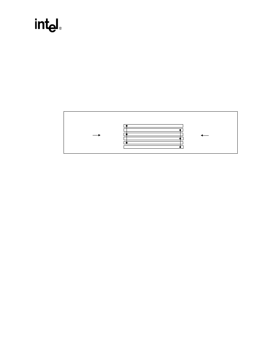
When possible, fill in unused areas of the signal planes with solid copper and attach them with
vias to a VCC or ground plane that is not located adjacent to the signal layer. This technique is
referred to as signal layer filling and can improve capacitive coupling of the power planes
(refer to
.
2.6
Magnetic “Safe Zone”
•
Void power and ground planes directly under the magnetics. Use chassis ground in the area
from the magnetics to the RJ-45 connector.
•
Keep high-speed signals out of the area between the LXT971A and the magnetics.
•
Do not route any digital signals between the LXT971A and the RJ-45 connectors at the edge of
the board.
2.7
Differential Signal Layout
•
Route differential pairs close together and away from other signals.
•
Keep both traces of each differential pair as identical to each other as possible.
•
Keep each differential pair on the same plane.
•
Minimize vias and layer changes.
•
Keep transmit and receive pairs away from each other. Run orthogonally, or separate with a
ground plane layer. One recommendation to maintain this separation is to place all
components for the transmit circuit on one side of the board, and all components for the
receive circuit on the other side of the board.
2.8
BGA Layout Considerations
Designing with a PBGA package requires special attention to spacing of pads and routing of
signals. The LXD971 Demo Board is designed with careful consideration to trace widths and
signal routing. The pinout for the LXT971A ensures that the MII signals can be routed on one side
Figure 1. Signal Layer Filling
Layer 1
Layer 2
Layer 3
Layer 4
Layer 5
Layer 6
Layer Name
Plane Fill
VCC
GND
VCC
GND
Signal 1
Signal 4
GND Layer
VCC Layer
Signal 2
Signal 3
Layers 1 and 3
connected to
VCC
Layers 2 and 4
connected to
GND
LXT971A/972A 3.3V PHY Transceivers Design and Layout Guide
10
Application Note
Document #: 249016
Revision #: 003
Rev. Date: November 1, 2001
of the chip and the twisted-pair or fiber signals can be routed on the other side of the chip without
crossing traces. 6 mils wide traces are used between the pads of the chip for routing and 8 mils
wide traces are used outside the boundaries of the chip for routing the signals. This ensures proper
spacing for grouping and routing of all the signals to their respective sections.
2.9
Boundary Scan Interface
The LXT971A supports an IEEE 1149.1 Boundary Scan Test Interface for board-level testing. This
interface consists of five pins (TMS, TDI, TDO, TRST, and TCK). Boundary Scan pins have
internal termination and may be left floating when not in use. The BSDL file is available by
contacting your local sales office or by accessing the Intel website at www.intel.com.
2.10
System Clock Requirements
The LXT971A clock circuit requires a 25 MHz ±100 ppm reference clock (REFCLK) that must be
enabled at all times. Characteristics of the LXT971A clock include:
•
Duty cycle distortion no greater than 35 to 65%
•
TTL voltage levels (V
OH
> 2.0V)
The reference clock input is used to generate signals and recover receive signals. It may be
provided by either of two methods: connecting a crystal across the oscillator pins (XI and XO), or
connecting an external clock source to pin XI. The connection of a clock source to the XI pin
requires the XO pin to be left open. A crystal-based clock is recommended over a derived clock
(for example, PLL-based) to minimize transmit jitter.
Regardless of clock source, careful consideration should be given to physical placement, board
layout, and signal routing of the source to maintain the highest level of signal integrity. See the
“Clock Layout Guidelines” on page 10
for more details.
A crystal is typically used in NIC applications. An external 25 MHz clock source, rather than a
crystal, is frequently used in switch applications.
lists the crystals and crystal oscillators
recommended for use with the LXT971A and LXT972A.
2.10.1
Clock Layout Guidelines
•
Keep the clock traces as short as possible.
•
Route the clock traces adjacent to an unbroken ground plane.
•
Use a multi-output clock driver when driving multiple inputs with a single oscillator.
•
Individually terminate point-to-point interconnects to every clock load. Series termination is
the most common termination technique.
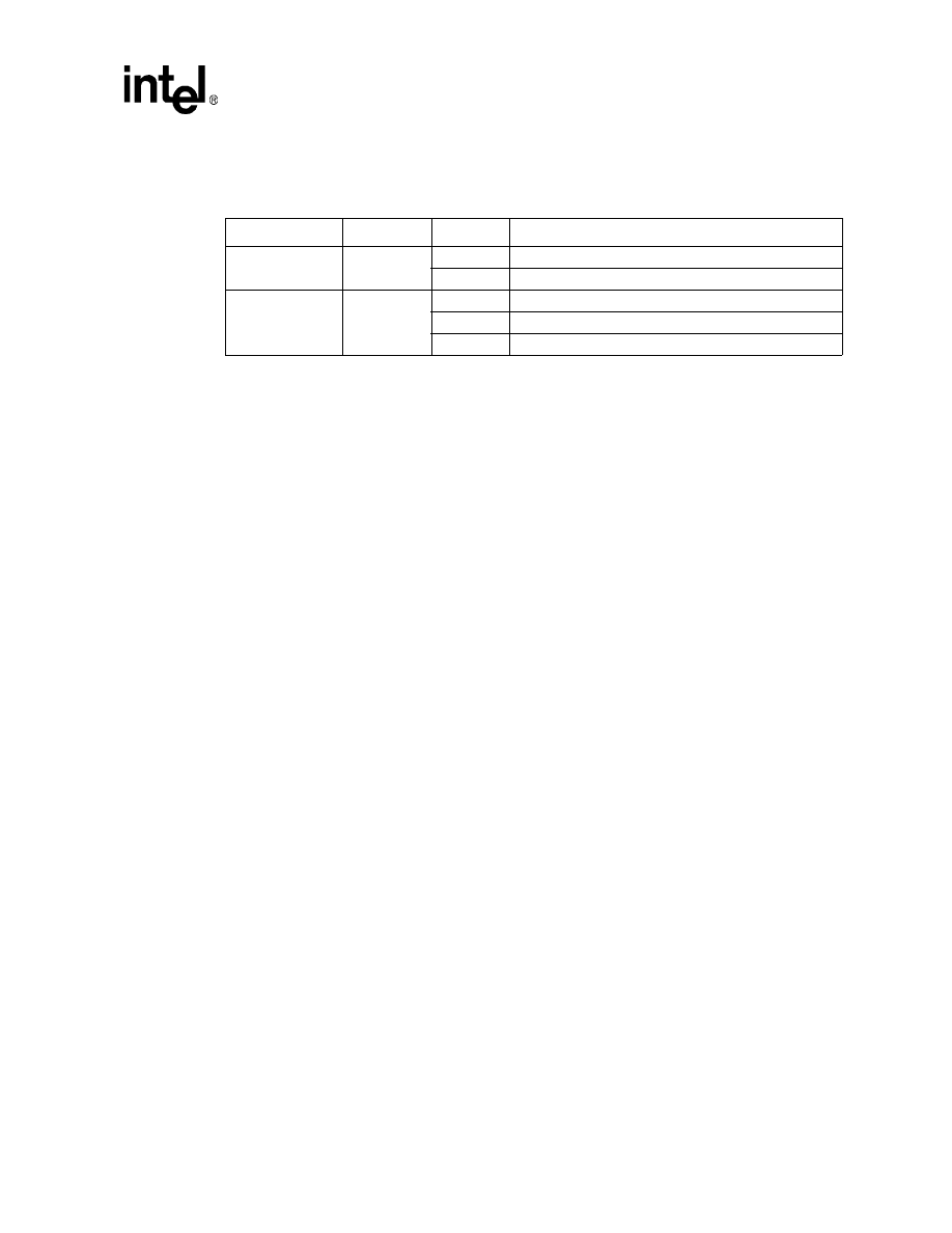
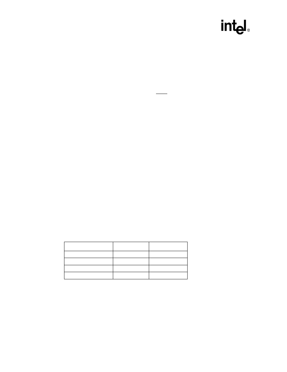
Table 1. Crystals/Crystal Oscillators
Manufacturer
Part Number
Type
Epson (Surface Mount)
MA-505
Crystal
Caliber (Through Hole)
AA18C1
Crystal
JDR
OSC250
Crystal Oscillator
CTS
MX045
Crystal Oscillator

LXT971A/972A 3.3V PHY Transceivers Design and Layout Guide
Application Note
11
Document #: 249016
Revision #: 003
Rev. Date: November 1, 2001
3.0
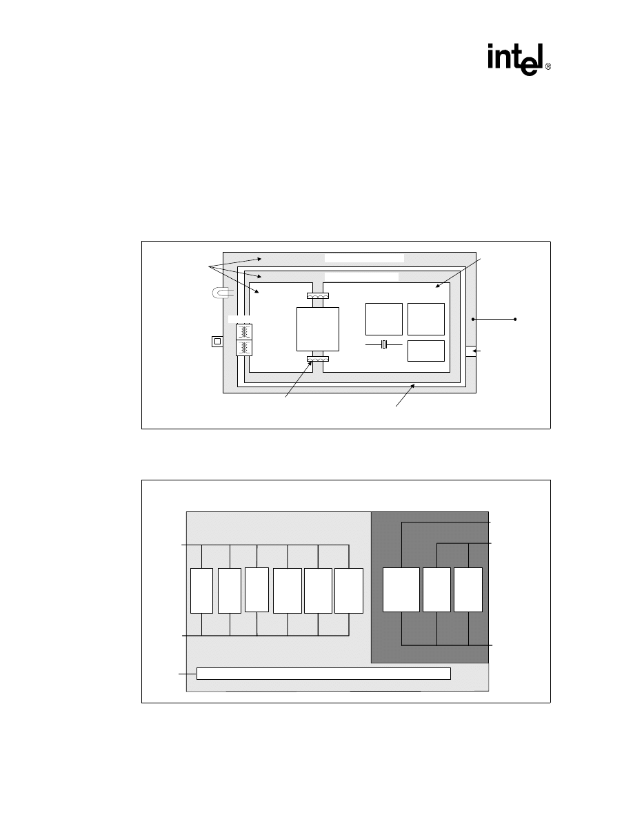
Power and Ground Design
3.1
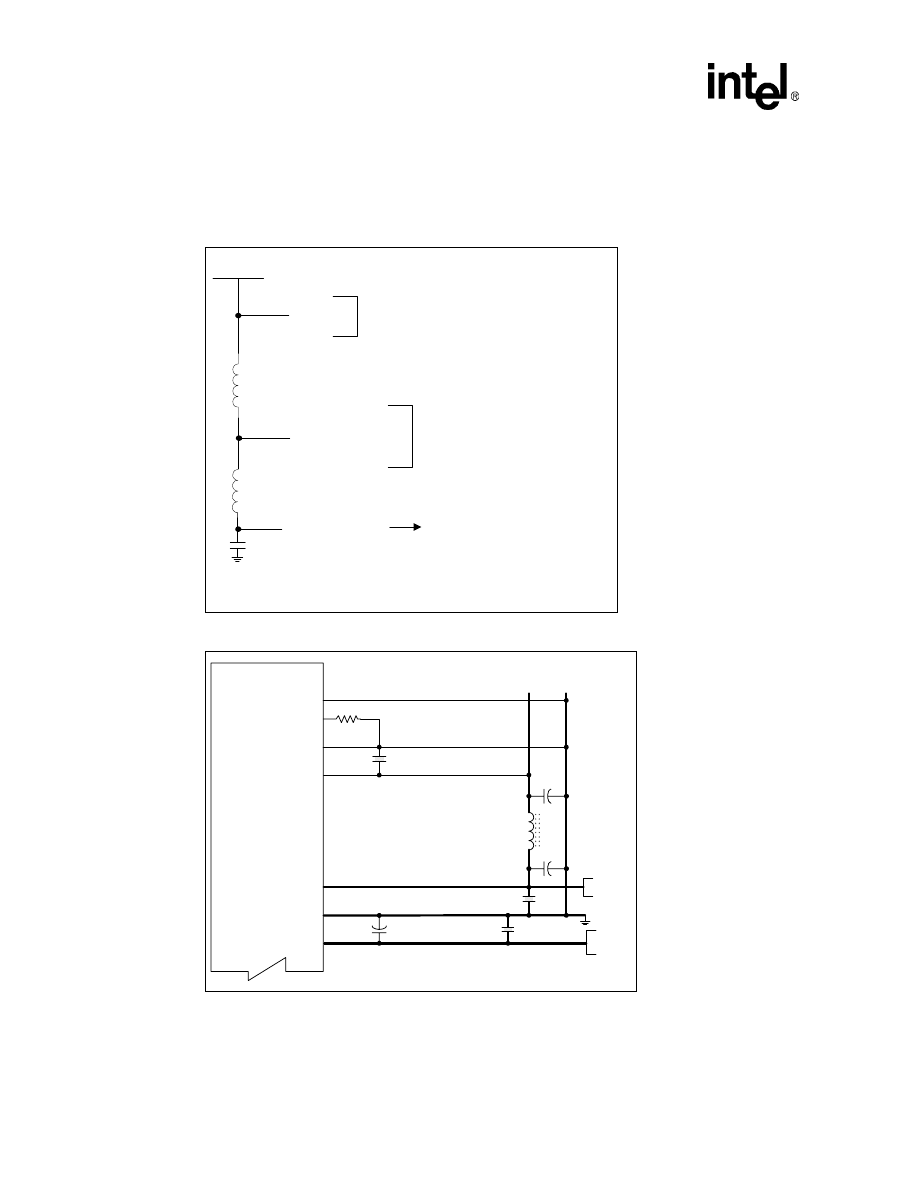
Power and Ground Planes
For high-speed communications design, the power and ground planes may be conceptually divided
into four regions (the analog and digital power planes and the chassis and signal ground planes) as
shown in
3.1.1
Power Planes
3.1.1.1
Analog VCC Plane
The analog power region extends from the magnetics back to the LXT971A. The power plane in
this area should be filtered. Only components and signals pertaining to the analog interface should
be placed or routed through this region. The analog plane supplies power to the VCCA pins of the
LXT971A as shown in
3.1.1.2
Digital VCC Plane
The digital power region extends from the MII interface of the LXT971A through the rest of the
board. Good design practices listed in the previous section should be followed throughout this area.
The digital plane supplies power to VCCD and VCCIO as shown in
. External
components (oscillators and the MAC) are also supplied from the digital plane.
3.1.2
Ground Planes
3.1.2.1
Signal Ground
The signal ground region should be one continuous, unbroken plane extending from the magnetics
through the rest of the board.
Signal ground planes often have high-frequency noise caused by returning signal currents. While
these high-frequency fluctuations are too small to cause issues in the digital circuits, they are large
enough to exceed FCC limits and are often coupled onto signals running outside the digital block.
Using chassis ground minimizes high-frequency noise in the logic ground plane.
3.1.2.2
Chassis Ground
A chassis ground plane can be added to the layer stack. Place this plane directly next to a signal
ground plane to create a very tight capacitive coupling between the two planes. The chassis plane
should then be multi-point connected to the external chassis.
Chassis ground can also be combined with the signal ground layer. For isolation, place a “moat”
around the signal ground plane to separate signal ground from chassis ground.
The chassis ground region extends from the front edge of the board (RJ-45 connectors) to the
magnetics, and around the entire perimeter of the board. No signals should pass through this region
except for external interfaces and LED signals.
LXT971A/972A 3.3V PHY Transceivers Design and Layout Guide
12
Application Note
Document #: 249016
Revision #: 003
Rev. Date: November 1, 2001
3.1.3
Avoiding Loop Antenna
When laying out ground planes, special care must be taken to avoid creating loop antenna effect.
•
Run all ground planes as solid square or rectangular regions.
•
Avoid creating loops with ground planes around other planes. The only exception to this rule is
chassis ground as shown in
•
Ensure the chassis ground loop (running the perimeter of the board) is voided at some point.
•
Ensure the gap of the voided area in chassis ground is large enough to prevent a ground loop.
Figure 2. Power and Ground Placement
Analog
VCC
Plane
Digital VCC Plane
MAC
Ferrites
SCC
RAM
Ferrites
LXT971A
Signal Ground Plane
Optional isolation Area
Magnetics
RJ-45
LEDs
Tie to Safety/
Earth Ground
Void area to
prevent loop
antenna effect
Keep all high-
speed digital
logic signals out
of the analog
power plane
and ground
planes
Keep all high-
speed digital
logic signals
inside the
digital power
plane
Filter the analog and
digital power planes
with ferrite beads
Chassis Ground Plane
Figure 3. Internal Routing of Analog and Digital Power Signals
Substrate
Digital Circuitry
Analog Circuitry
Rcvrs
Txmtrs
100M
Rx
PLL
GND
GND
VCCA
(3.3V)
10M
Rx &
Tx
PLLs
Bias
100M
Tx
PLL
GND
Clock
Digital
Logic
MII
Interface
VCCIO
(3.3V or 2.5V)
VCCD
(3.3V)
LXT971A/972A 3.3V PHY Transceivers Design and Layout Guide
Application Note
13
Document #: 249016
Revision #: 003
Rev. Date: November 1, 2001
3.2
Design Considerations
Power supply ripple and digital switching noise can be created by:
•
Poorly-regulated or over-burdened power supplies
•
Data busses running at high clock rates
•
DC-to-DC converters
Noise created by these sources can be coupled into the transmitter and receiver and out onto the
network. Coupling may also occur through the LXT971A analog power and ground pins or other
termination circuits (magnetic center taps).
See the Network Interface section on page 16
. This
condition contributes to EMI and data corruption.
Use the criteria in
for evaluating acceptable noise levels in the analog region of the power
and ground planes.
3.3
Design Implementation
Following good general design and layout guidelines prevents most common signal and noise
issues. The following recommendations apply to the design and layout of the power and ground
planes:
•
Divide the VCC plane into two sections as shown in
(analog and digital).
The break between the two planes should run under the device.
•
When dividing the VCC plane, it is not necessary to add extra layers to the board. Simply
create moats or cut-out regions in existing layers.
•
Join the digital and analog sections at one or more points by ferrite beads. Ensure the
maximum current rating of each bead is at least 150% of the nominal current that is expected
to flow through it. Each LXT971A and its transformer draws a maximum of 65 mA from the
analog supply so beads rated at 100 mA should be used. See
for current
load listings.
•
Place a bulk capacitor (10
µF) on each side of each ferrite bead to stop switching noise from
traveling through the ferrite.
•
For designs with multiple LXT971As, it is acceptable to supply all from one analog VCC
plane. This plane can be joined to the digital VCC plane at multiple points, with a ferrite bead
at each one. It is also acceptable to create an individual analog VCC mini-plane for each
device.
•
To improve EMI performance, use a ferrite bead between the analog voltage plane and the
magnetic transmit center tap as shown in
Table 2. Criteria for Analog Noise Levels
Noise Level
Acceptability
Under 50 mV
Acceptable
50 mV to 80 mV
Marginally Acceptable
Above 80 mV
Unacceptable
LXT971A/972A 3.3V PHY Transceivers Design and Layout Guide
14
Application Note
Document #: 249016
Revision #: 003
Rev. Date: November 1, 2001
•
Place a high-frequency bypass cap (.01
µf) near each VCC pin as shown in
•
Place a 10
µF bulk capacitor between VCCIO and GND close to the device.
•
Use a continuous, unbroken ground plane.
Figure 4. Power Supply Current
Figure 5. Power and Ground Decoupling
125 mA Total
VCC
Ferrite bead
rated at 100 mA
VCCD
VCCIO
VCCA - 35 mA
Direct supply to the LXT971A
Analog Plane
60 mA
Ferrite bead
rated at 50 mA
To TPO magnetic
center-tap
VCCA - 30 mA
Direct supply to the LXT971A
Digital Plane
.01
µ
F
Current ratings shown are estimated maximums.
RBIAS
GND
VCCA
.01
µ
F
22.1k
Ω 1%
GND
VCCD
.01
µ
F
Ferrite
Bead
10
µ
F
LXT971A
VCCIO
+3.3V
+ 2.5V or
3.3V
.01
µ
F
GND
+
10
µ
F
+
10
µ
F
+
LXT971A/972A 3.3V PHY Transceivers Design and Layout Guide
Application Note
15
Document #: 249016
Revision #: 003
Rev. Date: November 1, 2001
4.0
MII Interface
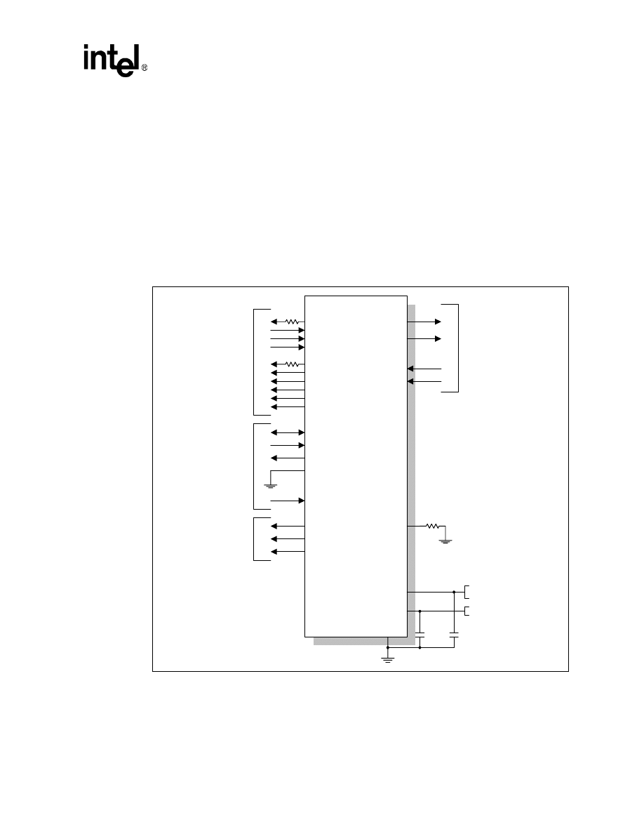
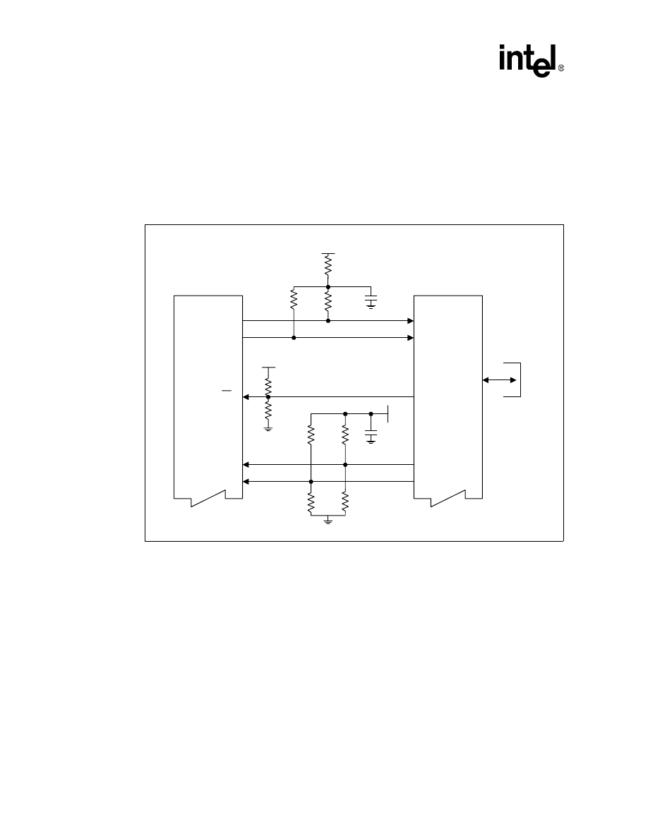
The LXT971A MII uses nine signals to pass received data to the MAC (RXD<3:0>, RX_CLK,
RX_DV, RX_ER, COL, and CRS). There are seven signals used to transmit data from the MAC
(TXD<3:0>, TX_CLK, TX_EN, and TX_ER). The MII operates at 25 MHz for 100 Mbps links
and 2.5 MHz for 10 Mbps links.
The LXT971A MII has high output impedance (250 - 350
Ω) and normally only requires
termination on the data and status output signals in designs with long traces (>3 inches). Series
termination resistors are strongly advised on the RX_CLK and TX_CLK signals to minimize
reflections. Place the resistor as close to the device as possible. Use a software trace termination
package to select an optimal resistance value for the specific trace. If this is not possible, use a 50
Ω
shows the MII interface for the LXT971A.
Figure 6. LXT971A MII Interface
TX_CLK
COL
TXD_<3:0>
TX_EN
MII
Data
I/F
MDDIS
MDC
MDINT
MDIO
MII
Mgmt
I/F
LED/CFG_2
LED/CFG_1
LED/CFG_3
Hardware
Control I/F
& Port LEDs
ADD<4:0>
TPOP
TPON
TPIP
TPIN
Network
I/F
VCCIO
+3.3V or +2.5V
VCCD
+3.3V
GND
.01
µ
F
TX_ER
RX_CLK
RX_DV
RX_ER
RXD_<3:0>
CRS
RBIAS
22.1k
Ω 1%
.01
µ
F
LXT971A/972A 3.3V PHY Transceivers Design and Layout Guide
16
Application Note
Document #: 249016
Revision #: 003
Rev. Date: November 1, 2001
5.0
Network Interfaces
5.1
Twisted-Pair Interface
The twisted-pair interface consists of magnetics, connectors, and termination networks for the
receiver and transmitter. The LXT971A requires magnetics with a 1:1 turns ratio for both the
receive and the transmit transformers. A circuit known as a “Bob Smith” termination (
see
) may be used to ground unused signal pairs.
5.1.1
Receive Interface Circuit
The receive interface circuit consists of magnetics including a main winding, common-mode
choke, and external termination resistance matching the line impedance.
5.1.1.1
Common-Mode Choke
Receive magnetics generally include a common-mode choke. Some vendors place this filter on the
line (primary) side of the main winding; others place it on the device (secondary) side. Either
approach is acceptable.
If using a magnetic with the common-mode choke on the device side, do not attach a bypass cap
from the device-side center tap to ground. Noise from the ground can couple through the cap into
the center tap, bypassing the common-mode choke, and cause EMI problems.
5.1.1.2
Termination Circuitry
shows the recommended receive termination. A 100
Ω load is placed across the receive
TPFIP/TPFIN input pair. This is accomplished using two 50
Ω resistors with a common-mode
bypass capacitor (0.01
µF) to ground. This provides additional common-mode shielding (when the
reference ground is quiet) and a potential discharge path for ESD events on the receiver.
The 270 pF coupling capacitors work with the receiver circuitry of the LXT971A improving the
signal-to-noise ratio for the receiver at long line lengths. Place the 270 pF series coupling
capacitors as close to the LXT971A as possible.
Figure 7. Receive Interface Circuitry
1:1
Main
Winding
CM
Choke
Magnetics
RJ-45
Chassis GND
1:1
Main
Winding
CM
Choke
To Chip
To Line
Alternate Magnetics
Secondary
Primary
Secondary
Primary
GNDR
0.01
µ
F
TPFIN
TPFIP
LXT971A
50
Ω 1%
50
Ω 1%
270 pF 5%
270 pF 5%
1
2
0.01
µ
F/2kV
1. Place these capacitors as close to the LXT971A as possible.
2. Magnetics without a receive pair center tap do not require a 2 kV termination.

LXT971A/972A 3.3V PHY Transceivers Design and Layout Guide
Application Note
17
Document #: 249016
Revision #: 003
Rev. Date: November 1, 2001
5.1.2
Transmit Interface Circuit
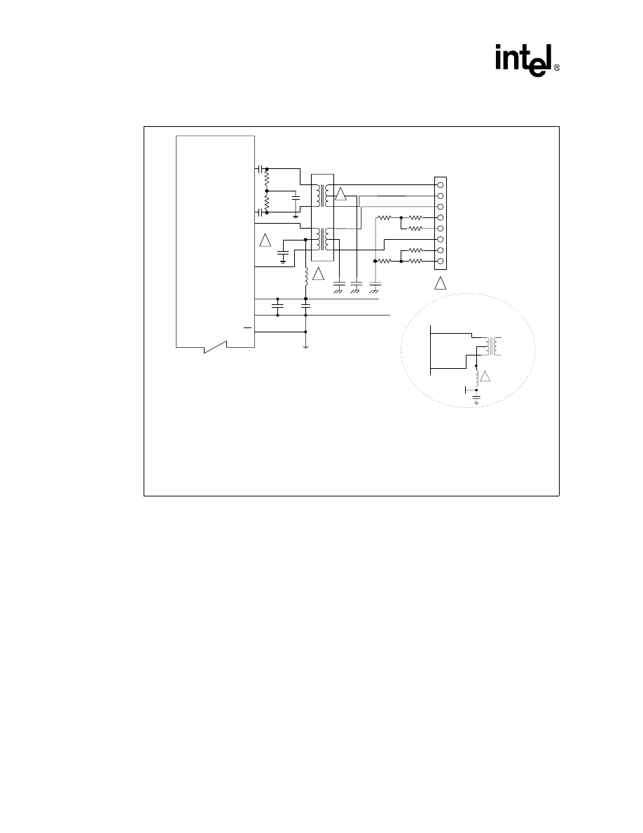
The recommended termination circuitry with the magnetics on the transmit interface for both
Switch and NIC RJ-45 configurations are shown in
Figure 8A and Figure 9A
. This circuit includes:
•
Magnetic center tap (device-side) tied to VCCA via a ferrite bead and bypassed to GND using
.01
µF capacitor
•
One ferrite bead per device, rated at 50 mA to supply center tap current
Designs requiring reduced power can be supplied with an alternative 2.5V power source on the
magnetics center tap (device side) instead of VCCA as shown in
. This
saves up to 25 mW of system power.
The output stage of the transmitter shown in
is designed to match the
100
Ω characteristic impedance of an unshielded CAT5 twisted-pair wire. The external resistor that
is typically required for impedance matching is integrated in the transmitter of the LXT971A. The
internal termination provides a constant current reference in both 10BASE-T and 100BASE-TX
applications and meets all IEEE transmitter requirements such as return loss, while reducing
external component requirements. It has no impact in fiber designs
5.1.2.1
Common-Mode Choke
The transmit magnetics always include a common-mode choke. Some vendors place this choke on
the line-side (secondary) of the main winding while others place it on the device-side (primary). A
few vendors include two transmit chokes
one on each side of the main winding.
The line-side center tap can be bypassed to chassis ground, but this should be carefully evaluated in
the system application. Bypassing both center taps of the transmit winding may produce
undesirable results by creating a low-impedance AC coupling between the chassis ground and
circuit ground. Consider potential noise sources and ground plane characteristics when evaluating
bypass options.
LXT971A/972A 3.3V PHY Transceivers Design and Layout Guide
18
Application Note
Document #: 249016
Revision #: 003
Rev. Date: November 1, 2001
Figure 8. Typical Twisted-Pair Interface - Switch
TPFIP
TPFIN
RJ-45
* = 0.001
µ
F / 2.0 kV
T
o
T
w
is
te
d
-Pa
ir
N
e
tw
o
rk
3
6
1
2
1:1
LXT971A
50
Ω
50
Ω
50
Ω
50
Ω
50
Ω
50
Ω
4
5
8
7
1:1
1
TPFOP
TPFON
VCCA
GND
0.1
µ
F
.01
µ
F
2
270 pF 5%
270 pF 5%
0.01
µ
F
50
Ω 1%
50
Ω 1%
*
*
3
SD/TP
4
A
0.1
µ
F
1:1
1
TPFOP
TPFON
2.5V
Reduced-Power
Transmit Interface
Circuitry
B
.01
µ
F
1. Center tap current may be supplied from 3.3V VCA as shown. Additional power savings may be
realized by supplying the center tap from a 2.5V current source. A separate ferrite bead (rated at
50 mA) should be used to supply center tap current.
2. The 100
Ω
transmit load termination resistor typically required is integrated in the LXT971A.
3. Magnetics without a receive pair center tap do not require a 2 kV termination.
4. RJ-45 connections shown are for a standard switch application. For a standard NIC RJ-45
setup, see
.
LXT971A/972A 3.3V PHY Transceivers Design and Layout Guide
Application Note
19
Document #: 249016
Revision #: 003
Rev. Date: November 1, 2001
5.1.2.2
Meeting IEEE Requirements
Designers should focus on two key areas to optimize return loss performance with the LXT971A.
First, minimize shunt capacitance on the board, and second, carefully select the magnetics.
Adherence to the following guidelines helps to ensure each design meets IEEE requirements for
the 100BASE-TX PMD layer as called out in the ANSI X3.263 specification.
Guidelines for Reducing System Shunt Capacitance.
•
Avoid multiple layer changes in TPFON/P and TPFIN/P signal routing.
•
Keep the magnetics as close as possible to the LXT971A, and keep TPFOP and TPFON traces
as short as possible.
•
In multi-chip applications, use quad magnetics optimized for dual-high RJ-45 connectors to
allow the most compact layout.
•
Use the termination circuit shown in
.
•
Provide EMI shielding by placing a ground plane under TPFOP and TPFON and the
magnetics. To achieve an optimum layout for EMI and return loss performance, place the
shielding ground plane two to three layers away to minimize shunt capacitance between the
traces and the ground plane.
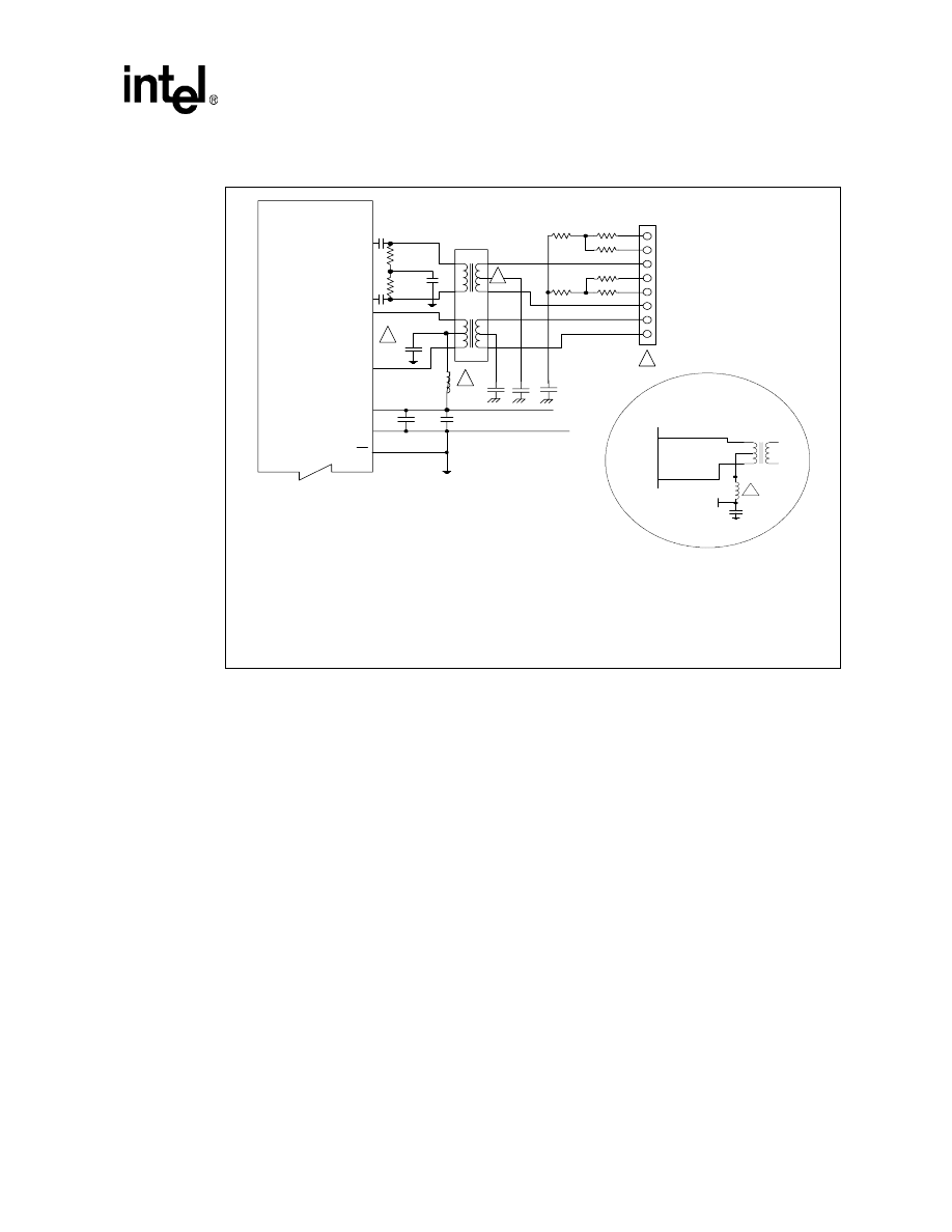
Figure 9. Typical Twisted-Pair Interface - NIC
TP F IP
T P F IN
* = 0 .0 0 1
µ
F / 2.0 k V
To
Tw
is
te
d
-P
a
ir
N
e
tw
o
rk
1 :1
LX T 97 1A
1 :1
1
T P F O P
T P F O N
V C C A
G N D
0 .1
µ
F
.0 1
µ
F
2
2 7 0 p F 5%
2 7 0 p F 5%
0.0 1
µ
F
5 0
Ω 1%
5 0
Ω 1%
*
*
3
S D /T P
6
3
8
7
5
4
1
2
5 0
Ω
5 0
Ω
5 0
Ω
RJ -4 5
5 0
Ω
5 0
Ω
5 0
Ω
4
A
0 .1
µ
F
1 :1
1
T P FO P
T P FO N
2 .5V
R e d u c ed -Po w e r
T r an sm it In te rfa c e
C irc u itr y
B
.0 1
µ
F
1. Center tap current may be supplied from 3.3V VCA as shown. Additional power savings may be
realized by supplying the center tap from a 2.5V current source. A separate ferrite bead (rated at
50 mA) should be used to supply center tap current.
2. The 100
Ω
transmit load termination resistor typically required is integrated in the LXT971A.
3. Magnetics without a receive pair center tap do not require a 2 kV termination.
4. RJ-45 connections shown are for a standard NIC application. Tx/Rx crossover may be required
for repeater and switch applications.
LXT971A/972A 3.3V PHY Transceivers Design and Layout Guide
20
Application Note
Document #: 249016
Revision #: 003
Rev. Date: November 1, 2001
5.1.3
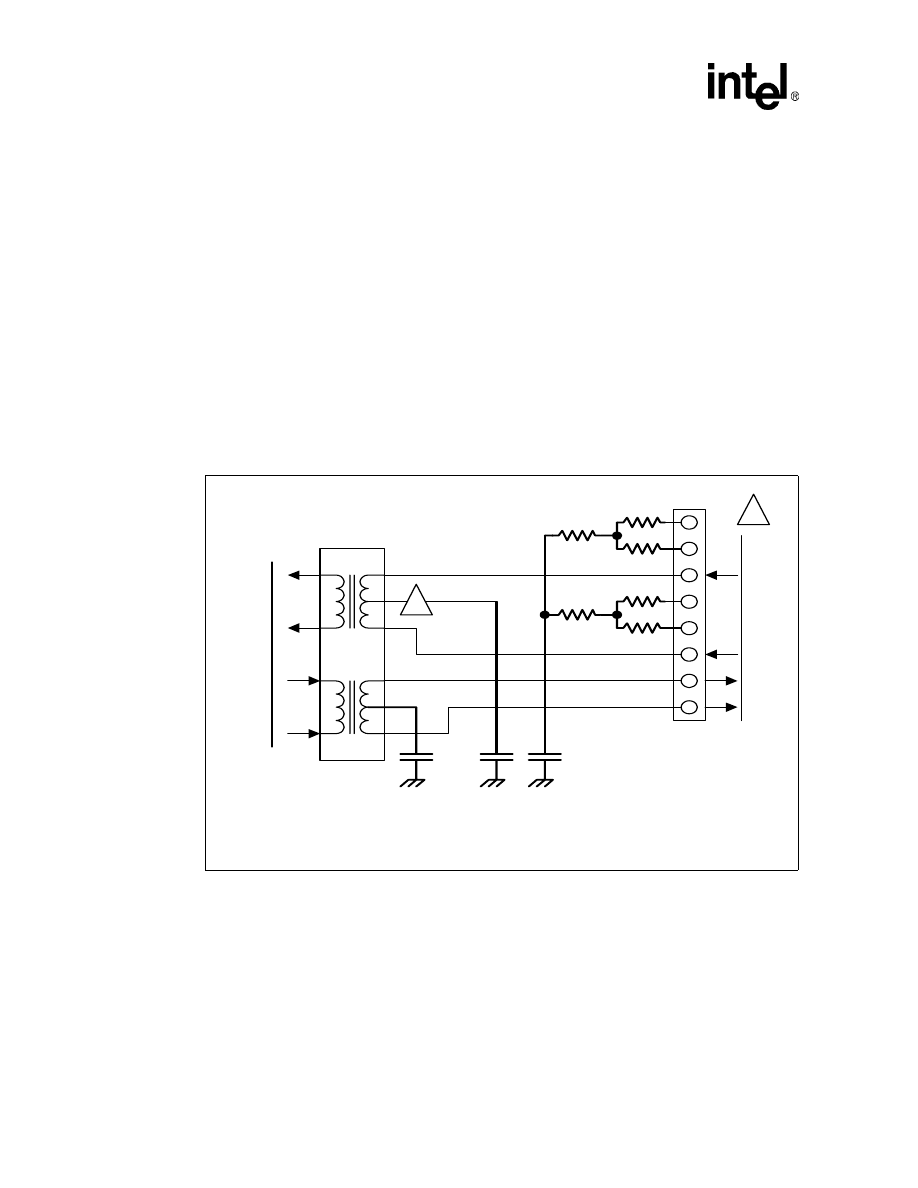
Bob Smith Termination
A "Bob Smith" termination is provided for the unused signal pairs of the twisted-pair interface (RJ-
45 pins 4, 5, 7, and 8) and the media-side center taps. The circuit is used to enhance EMI and ESD
performance of the system. Although there are many variations of this technique, one common
implementation is shown in
. Note the signals are referenced to chassis ground rather than
circuit ground.
A Bob Smith termination can be broken down into two circuits. One circuit provides termination
for the unused signal pairs of the twisted-pair interface. The unused pairs are connected together
through a 75
Ω impedance matching circuit to chassis ground through a 0.001 µF, 2 kV capacitor.
The capacitor provides a discharge path for noise immunity on the unused pairs.
The second circuit provides termination for the media-side center taps and is comprised of
individual 0.001
µF, 2 kV capacitors to chassis ground. Separate capacitors are used for the receive
and transmit center taps. This improves isolation by eliminating the low impedance path between
receiver and transmitter that would exist if a single common cap were used. The capacitors provide
a high-frequency path to ground, enhancing ESD and EMI performance.
Figure 10. Bob Smith Termination Circuit
RJ-45
50
Ω
50
Ω
50
Ω
50
Ω
50
Ω
T
o
/ F
ro
m
Tw
is
te
d
-P
a
ir
L
in
e
6
5
4
3
2
1
8
7
RX
TX
To
/
Fr
o
m
C
h
ip
50
Ω
0.001
µ
F
2kV
*
*
*
* =
1
2
1. RJ-45 connections shown for standard NIC. TxRx crossover may be required for switch
applications.
2. Magnetics without a receive pair center tap do not require a 2 kV termination.
LXT971A/972A 3.3V PHY Transceivers Design and Layout Guide
Application Note
21
Document #: 249016
Revision #: 003
Rev. Date: November 1, 2001
5.2
Magnetic Requirements
The LXT971A requires a 1:1 ratio for both the receive transformers and the transmit transformers.
The transmit isolation voltage should be rated at 1.5 kV to protect the circuitry from static voltages
across the connectors and cables. Refer to
for magnetics requirements.
Refer to
for a list of magnetic manufacturers and part numbers. This list constitutes a
reference only and is not a recommendation. The system designer must ensure that all components,
both individually and collectively, are suitable for the intended application.
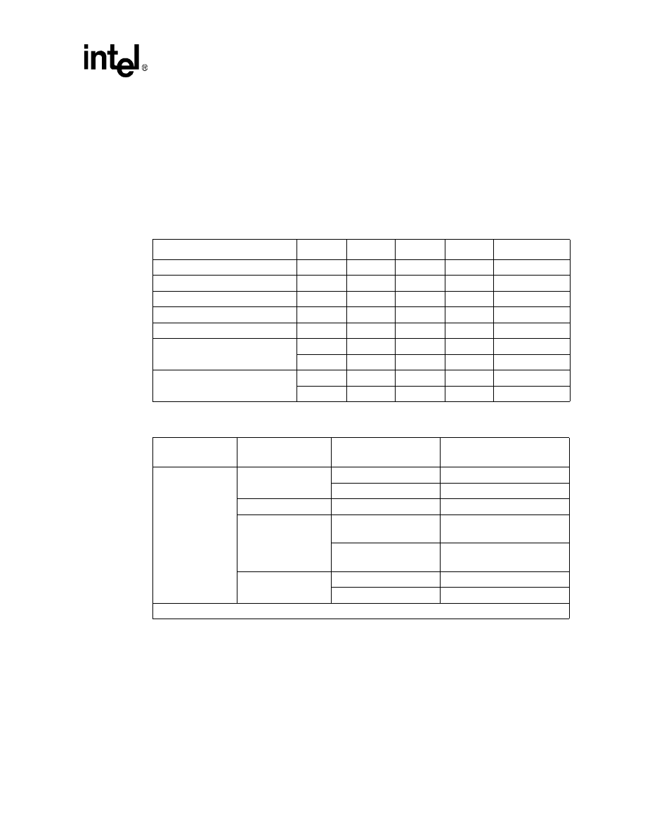
Table 3. Magnetic Requirements
Parameter
Min
Nom
Max
Units
Test Condition
Rx turns ratio
–
1 : 1
–
–
–
Tx turns ratio
–
1 : 1
–
–
–
Insertion loss
0.0
0.6
1.1
dB
–
Primary inductance
350
–
–
µ
H
–
Transformer isolation
–
1.5
–
kV
–
Differential to common mode
rejection
40
–
–
dB
.1 to 60 MHz
35
–
–
dB
60 to 100 MHz
Return Loss
-16
–
–
dB
30 MHz
-10
–
–
dB
80 MHz
Table 4. Magnetic Manufacturers
Port/Ratio
Manufacturer
1
Temperature
Part Numbers
Single-Port
Rx = 1:1
Tx = 1:1
B
EL
F
USE
Commercial
S558-5999-T7
Industrial
S558-5999-T5
D
ELTA
Industrial
LF8416
H
ALO
Commercial
TG110-S050N2
TG110-S050P2
Industrial
TG110-E050N5
TG22-E150NL
P
ULSE
Commercial
H1102
Industrial
Hx1148
1. Device manufacturers may have additional magnetics with varying pinouts.
LXT971A/972A 3.3V PHY Transceivers Design and Layout Guide
22
Application Note
Document #: 249016
Revision #: 003
Rev. Date: November 1, 2001
5.3
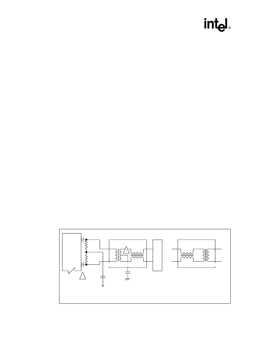
Fiber Interface
The fiber interface consists of two pseudo-ECL (PECL) signal pairs that attach to an external fiber
optic transceiver. Both fiber data pairs (TPFOP/N and TPFIP/N) should be DC-coupled to the fiber
transceiver.
shows both circuits. The combinations of bias resistors shown provide the ideal biasing
points for an equivalent load impedance of 50
Ω.
Figure 11. Fiber Interface Circuit
TPFON
TPFOP
TPFIN
TPFIP
50
Ω
50
Ω
Fiber Txcvr
T
o
F
iber
N
e
tw
or
k
0.1
µ
F
82
Ω
82
Ω
130
Ω
130
Ω
0.1
µ
F
TD-
TD+
RD-
RD+
GND
GND
GND
SD/TP
LXT971A
SD
130
Ω
82
Ω
GNDD
VCCD
+3.3V
VCCD
+3.3V
VCCD
+3.3V
16
Ω

LXT971A/972A 3.3V PHY Transceivers Design and Layout Guide
Application Note
23
Document #: 249617
Revision #: 001
Rev. Date: November 1, 2001
Appendix A LXT971A Design and Layout Checklist
A.1
Power and Ground
A.1.1
Design
A.1.2
Layout
Ensure that the power and ground noise levels are below 50 mV
Ensure that the power supply is properly rated for the entire board load
Use bulk capacitors (4.7 - 10
µ
F) between the power and ground planes to minimize power
supply switching noise.
Filter and shield DC-DC converters, oscillators, etc.
Use an ample supply of .01
µ
F decoupling capacitors to reduce high-frequency noise on the
power and ground planes.
Join the digital and analog sections at one or more points by ferrite beads. Ensure the
maximum current rating of each bead is at least 150% of the nominal current that is expected
to flow through it. Each LXT971A and its transformer draws a maximum of 65 mA from the
analog supply, so beads rated at 100 mA should be used.
Place a bulk capacitor (10
µ
F) on each side of each ferrite bead to stop switching noise from
traveling through the ferrite.
Place a 10
µ
F bulk capacitor, close to the device, between VCCIO and GND.
Place a high-frequency bypass cap (.01
µ
F) near each VCC pin.
Avoid breaks in the ground plane, especially in areas where the ground plane is shielding high-
frequency signals.
Route high-speed signals above a continuous, unbroken ground plane.
When possible, fill in unused areas of the signal planes with solid copper and attach them with
vias to a VCC or ground plane that is not located adjacent to the signal layer. This technique is
referred to as signal layer filling and can improve capacitive coupling of the power planes.
Use a continuous, unbroken ground plane.

A.2
System Clock
A.2.1
Design
A.2.2
Layout
A.3
MII Interface
A.3.1
Design
A.4
Twisted-Pair Interface
A.4.1
Design
Ensure that the system clock is a 25 MHz + 100 ppm reference clock (REFCLK) that must be
enabled at all times.
Ensure that the duty cycle distortion is no greater that 35 to 65%.
Ensure that the TTL voltage levels are VOH > 2.0V.
If you have issues linking at 100 Mbps speeds, but can link at 10 Mbps, try implementing one
of the crystal or crystal oscillator devices specified in
before contacting
Intel Customer Support.
Keep the clock traces as short as possible.
Route the clock traces adjacent to an unbroken ground plane.
Use a multi-output clock driver when driving multiple inputs with a single oscillator.
Individually terminate point-to-point interconnects to every clock load. Series termination is the
most common termination technique.
The LXT971A MII have high output impedance (250 - 350
Ω
) and normally require termination
on the data and status output signals in designs with long traces (>3 inches).
Series termination resistors are strongly recommended on the RX_CLK and TX_CLK signals
to minimize reflections. Place the resistor as close to the LXT971A as possible.
Use a trace termination software modeling application to select an optimal resistance value for
the specific trace. If this is not possible, use a 50W resistor value.
Ensure that the RBIAS resistor is a 22.1 k
Ω
1% resistor to ground for internal reference current
setup. Place the resistor close to the LXT971A.
The LXT971A/LXT972A has integrated transmit termination and does not require external
100
Ω
termination to work properly.
If you have issues linking or communicating over the twisted-pair or fiber interface, please
verify that the proper termination values are populated on the board prior to escalating or
contacting Intel Customer Support.

LXT971A/972A 3.3V PHY Transceivers Design and Layout Guide
Application Note
25
Document #: 249617
Revision #: 001
Rev. Date: November 1, 2001
A.4.2
Layout
A.5
Fiber Interface
A.5.1
Design
A.5.2
Layout
A.6
Magnetics
A.6.3
Design
A.6.4
Layout
Route differential pairs close together and away from other signals.
Keep both traces of each differential pair as identical to each other as possible.
Keep each differential pair on the same plane.
Minimize vias and layer changes.
Keep transmit and receive pairs away from each other. Run orthogonally, or separate with a
ground plane layer. To maintain this separation, place all components for the transmit circuit on
one side of the board and all components for the receive circuit on the other side of the board.
To improve EMI performance, use a ferrite bead between the analog voltage plane and the
magnetic transmit center tap.
Sleep mode is not functional in fiber network applications.
If you have issues linking or communicating over the twisted-pair or fiber interface, please
verify that the proper termination values are populated on the board prior to escalating or
contacting Intel Customer Support.
Transmit isolation voltage should be rated at 1.5 kV to protect the circuitry from static voltages
across the connectors and cables.
Ensure that the magnetic transformer ratio is maintained with Rx = 1:1 and Tx = 1:1.
If using a magnetic with the common-mode choke on the device side, do not attach a bypass
cap from the device-side center tap to ground. Noise from the ground can couple through the
cap into the center tap, bypassing the common-mode choke, and cause EMI problems.
Void power and ground planes directly under the magnetics. Use chassis ground in the area
from the magnetics to the RJ-45 connector.
Keep high-speed signals out of the area between the LXT971A and the magnetics.
Do not route any digital signals between the LXT971A and the RJ-45 connectors at the edge of
the board.

LXT971A/972A 3.3V PHY Transceivers Design and Layout Guide
26
Application Note
Document #: 249617
Revision #: 001
Rev. Date: November 1, 2001
A.7
General Design
Validate the value of the RBIAS resistor with a DMM to ensure that the proper value has been
populated on the board.
Download the latest revision of the specification updated from the following URL (
http://
developer.intel.com/design/network/products/physlayer/index.htm#Transceivers
).
Identify your stepping using the topside markings of the chip, and implement the appropriate
workarounds necessary for your design.
Changes have been made to the existing documentation to include or clarify specifications or
explanations over the life of the document. Ensure that you have the latest revision of the
LXT971A and LXT972A Datasheets from the URL noted above if documentation is unclear or
the specification is missing.
Document Outline
- 1.0 General Description
- 2.0 General Design Guidelines
- 3.0 Power and Ground Design
- 4.0 MII Interface
- 5.0 Network Interfaces
- Appendix A LXT971A Design and Layout Checklist
Wyszukiwarka
Podobne podstrony:
Australian by design id 72410 Nieznany (2)
lecture 9 robust design id 2643 Nieznany
Akwarium typu Low id 54526 Nieznany
korektor mikro eq pcb id 740442 Nieznany
pole placement robot design id Nieznany
EMI reduct id 160731 Nieznany
Akwarium typu Low id 54526 Nieznany
Abolicja podatkowa id 50334 Nieznany (2)
4 LIDER MENEDZER id 37733 Nieznany (2)
katechezy MB id 233498 Nieznany
metro sciaga id 296943 Nieznany
perf id 354744 Nieznany
interbase id 92028 Nieznany
Mbaku id 289860 Nieznany
Probiotyki antybiotyki id 66316 Nieznany
miedziowanie cz 2 id 113259 Nieznany
LTC1729 id 273494 Nieznany
D11B7AOver0400 id 130434 Nieznany
więcej podobnych podstron