
DS04-27225-2E
FUJITSU SEMICONDUCTOR
DATA SHEET
ASSP For Power Management Applications
6
-ch DC/DC Converter IC with Synchronous
Rectifier
for Voltage Step-up and Step-down
MB3883
■
■
■
■
DESCRIPTION
The MB3883 is a 6-channel step-up/step-down DC/DC converter IC using pulse width modulation (PWM) and
synchronous rectification, designed for low voltage, high efficiency, and compact size. This IC is ideal for up
conversion, down conversion, and up/down conversion (using a step-up/step-down Zeta system with free input
and output settings).
The MB3883 can operate at low voltage levels, and has a wide supply voltage range from 1.7 V to 9 V.
The MB3883 is available in two packages, an LQFP-48P or a leadless BCC-48P formed with a contact electrode
pad only.
This is an ideal power supply for high-performance portable devices such as digital still cameras.
■
■
■
■
FEATURES
• Supports synchronous rectification (CH1, 2, 5)
• Supports for down-conversion and up/down Zeta conversion (CH1, 2)
Supports for up-conversion (CH5)
• Supports up-conversion (CH3, 4, 6)
• Low start-up voltage
: 1.7 V (CH6)
• Power supply voltage range
: 2.4 V to 9 V (CH6)
: 3.6 V to 9 V (CH1 to CH5)
• Built-in high-precision reference voltage circuit
:
±
1 %
• Wide operating oscillator frequency range with high-frequency capability : 100 kHz to 1 MHz
• Error amplifier output for soft start (CH1 to CH6)
• Totem-pole type output switch control circuit
■
■
■
■
PACKAGES
48-pin plastic LQFP
48-pad plastic BCC
(FPT-48P-M05)
(LCC-48P-M02)
MB3883
2
■
■
■
■
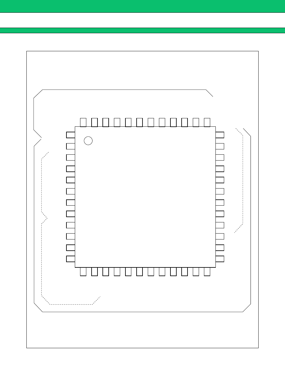
PIN ASSIGNMENTS
(TOP VIEW)
(FPT-48P-M05)
SWOUT
SWIN
FB6
−
IN6
C
+
IN6
DTC5
FB5
−
IN5
−
IN (A) 4
OUT (A) 4
FB4
−
IN4
1
2
3
4
5
6
7
8
9
10
11
12
36
35
34
33
32
31
30
29
28
27
26
25
DTC1
FB1
−
IN1
DTC2
FB2
−
IN2
DTC3
FB3
−
IN3
VB
CT
RT
−
IN (S) 4
DTC4
CS
VREF
GND
CSCP
VCC
CTL
CTL1, 2
CTL3
CTL4
CTL5
13
14
15
16
17
18
19
20
21
22
23
24
48
47
46
45
44
43
42
41
40
39
38
37
RB6
OUT6
OUT5-2
OUT5-1
GND (O)
OUT4
VCC (O)
OUT3
OUT2-2
OUT2-1
OUT1-2
OUT1-1
(CH5, CH6)
(CH1
∼
CH3)
(CH4)
Control block
Output block

MB3883
3
(TOP VIEW)
(LCC-48P-M02)
SWOUT
SWIN
FB6
−
IN6
C
+
IN6
DTC5
FB5
−
IN5
−
IN (A) 4
OUT (A) 4
FB4
−
IN4
−
IN (S) 4
1
2
3
4
5
6
7
8
9
10
11
12
13
37
36
35
34
33
32
31
30
29
28
27
26
25
OUT1-1
DTC1
FB1
−
IN1
DTC2
FB2
−
IN2
DTC3
FB3
−
IN3
VB
CT
RT
DTC4
CS
VREF
GND
CSCP
VCC
CTL
CTL1, 2
CTL3
CTL4
CTL5
14
15
16
17
18
19
20
21
22
23
24
48
47
46
45
44
43
42
41
40
39
38
RB6
OUT6
OUT5-2
OUT5-1
GND (O)
OUT4
VCC (O)
OUT3
OUT2-2
OUT2-1
OUT1-2
(CH5, CH6)
(CH1
∼
CH3)
(CH4)
Control block
Output block
MB3883
4
■
■
■
■
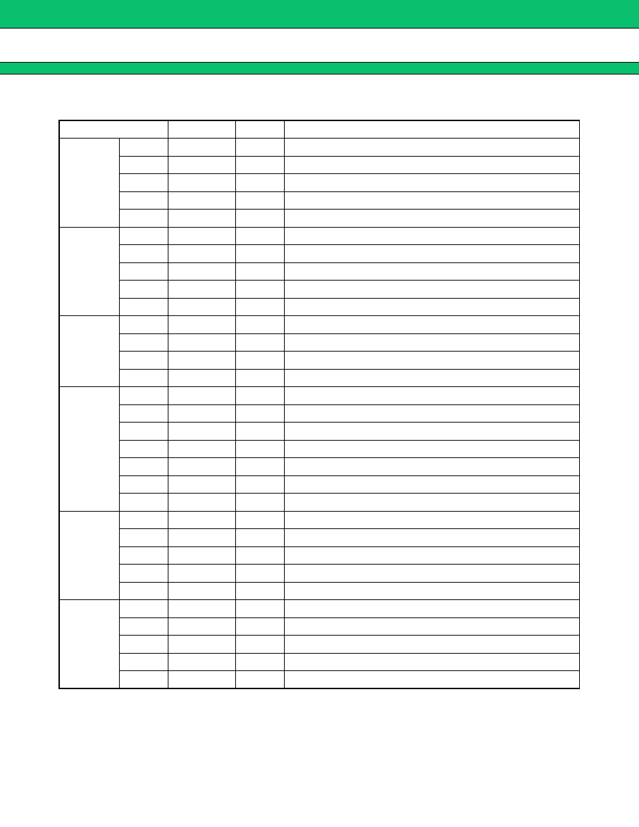
PIN DESCRIPTION
(Continued)
Pin No.
Symbol
I/O
Descriptions
CH1
35
FB1
O
Error amplifier output pin.
34
−
IN1
I
Error amplifier inverted input pin.
36
DTC1
I
Dead time control pin.
37
OUT1-1
O
Main side output pin.
38
OUT1-2
O
Synchronous rectifier side output pin.
CH2
32
FB2
O
Error amplifier output pin.
31
−
IN2
I
Error amplifier inverted input pin.
33
DTC2
I
Dead time control pin.
39
OUT2-1
O
Main side output pin.
40
OUT2-2
O
Synchronous rectifier side output pin.
CH3
29
FB3
O
Error amplifier output pin.
28
−
IN3
I
Error amplifier inverted input pin.
30
DTC3
I
Dead time control pin.
41
OUT3
O
Output pin.
CH4
11
FB4
O
Error amplifier output pin.
12
−
IN4
I
Error amplifier inverted input pin.
14
DTC4
I
Dead time control pin.
43
OUT4
O
Output pin.
9
−
IN (A) 4
I
Inverting amplifier input pin.
10
OUT (A) 4
O
Inverting amplifier output pin.
13
−
IN (S) 4
I
Short detection comparator inverted input pin.
CH5
7
FB5
O
Error amplifier output pin.
8
−
IN5
I
Error amplifier inverted input pin.
6
DTC5
I
Dead time control pin.
45
OUT5-1
O
Main side output pin.
46
OUT5-2
O
Synchronous rectifier side output pin.
CH6
3
FB6
O
Error amplifier output pin.
4
−
IN6
I
Error amplifier inverted input pin.
5
C
+
IN6
I
Soft start capacitor connection pin.
48
RB6
O
Output current setting resistor connection pin.
47
OUT6
O
Output pin.
MB3883
5
(Continued)
Pin No.
Symbol
I/O
Descriptions
OSC
25
RT
Triangular wave frequency setting resistor connection pin.
26
CT
Triangular wave frequency setting capacitor connection pin.
27
VB
O
Triangular wave oscillator regulator output pin.
Control
1
SWOUT
O
Output switch control circuit output pin.
2
SWIN
I
Output switch control circuit input pin.
20
CTL
I
Power supply, CH6 control pin.
“H” level : Power supply CH6 operating mode
“L” level : Standby mode
21
CTL1, 2
I
CH1, CH2 control pin.
When CTL1, 2 pin
=
“H” level
“H” level : CH1, CH2 operating mode
“L” level : CH1, CH2 OFF mode
22
CTL3
I
CH3 control pin.
When CTL3 pin
=
“H” level
“H” level : CH3 operating mode
“L” level : CH3 OFF mode
23
CTL4
I
CH4 control pin.
When CTL4 pin
=
“H” level
“H” level : CH4 operating mode
“L” level : CH4 OFF mode
24
CTL5
I
CH5 control pin.
When CTL5 pin
=
“H” level
“H” level : CH5 operating mode
“L” level : CH5 OFF mode
18
CSCP
Short protection circuit capacitor connection pin.
15
CS
CH1to CH5 soft start circuit capacitor connection pin.
Power
19
VCC
Reference voltage and control circuit power supply pin.
42
VCC (O)
Output circuit power supply pin.
16
VREF
O
Reference voltage output pin.
17
GND
Ground pin.
44
GND (O)
Output circuit ground pin.
MB3883
6
■
■
■
■
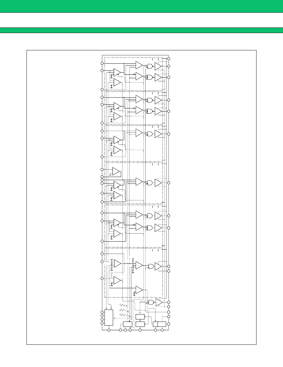
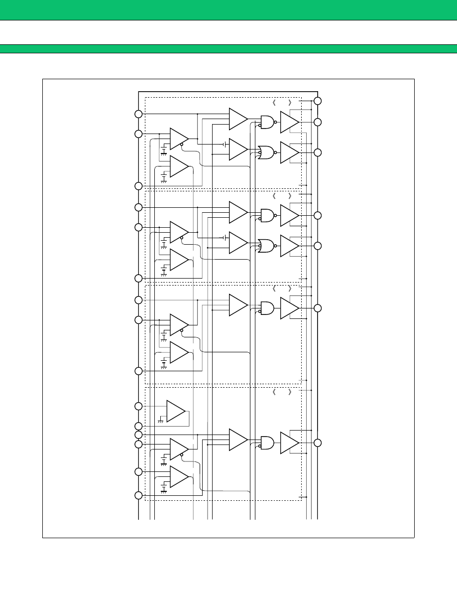
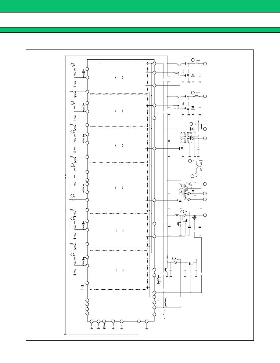
BLOCK DIAGRAM
PWM
Comp.
5-2
−
+
+
−
+
+
+
−
+
+
−
CH5
CH6
Drive
5-1
Drive
5-2
PWM
Comp.
5-1
VB1
Error
Amp.5
1.25 V
1.0 V
1.26 V
62.5 k
Ω
37 k
Ω
0.9 V
+
−
+
−
+
−
+
−
+
Drive
6
SW
Drive
PWM
Comp.6
Power
Comp.
0.9V
21
CTL1, 2
22
CTL3
23
CTL4
24
CTL5
1 SWOUT
44 GND (O)
2 SWIN
19 VCC
20
17
GND
16
VREF
18
CSCP
26
CT
25
RT
27
VB
15
CS
CTL
3
FB6
4
5
−
IN6
C
+
IN6
7
8
6
FB5
−
IN5
DTC5
45
46
OUT5-1
OUT5-2
47
48
OUT6
RB6
SCP
Comp.5
Error
Amp.6
37.5 k
Ω
(VB : 2 V)
(VB : 2 V)
0.74 V
63 k
Ω
CT1
CT2
CT
1.8 V
−
1.1 V
−
1.8 V
−
1.1 V
−
0.8 V
−
0.3 V
−
CS CTL
Logic
2 V
2.49 V
OSC
SCP
Ref
Power
ON/OFF
CTL
UVLO
(48 Pin)
PWM
Comp.
1-2
−
+
+
−
+
+
+
−
+
+
−
CH1
Drive
1-1
Drive
1-2
−
+
+
−
+
+
+
−
+
+
−
CH2
Drive
2-1
Drive
2-2
−
+
+
−
+
+
+
−
+
CH3
Drive
3
−
+
+
−
+
+
+
−
+
−
+
CH4
Drive
4
35
34
36
32
31
33
29
28
30
9
10
11
12
13
14
FB1
−
IN1
DTC1
FB2
−
IN2
DTC2
FB3
−
IN3
DTC3
−
IN (A) 4
OUT (A) 4
FB4
−
IN4
−
IN (S) 4
DTC4
42
37
38
39
40
41
43
VCC (O)
OUT1-1
OUT1-2
OUT2-1
OUT2-2
OUT3
OUT4
PWM
Comp.
1-1
VB1
PWM
Comp.
2-2
PWM
Comp.3
PWM
Comp.4
PWM
Comp.
2-1
VB1
Error
Amp.1
SCP
Comp.1
1.25 V
1.0 V
Error
Amp.2
1.25 V
1.0 V
SCP
Comp.2
Error
Amp.3
1.25 V
1.0 V
SCP
Comp.3
1.25 V
1.0 V
SCP
Comp.4
Error
Amp.4
INV
Amp.4
SCP
Comp.6
H : ON (Power/CH6)
L : OFF (Standby mode)
MB3883
7
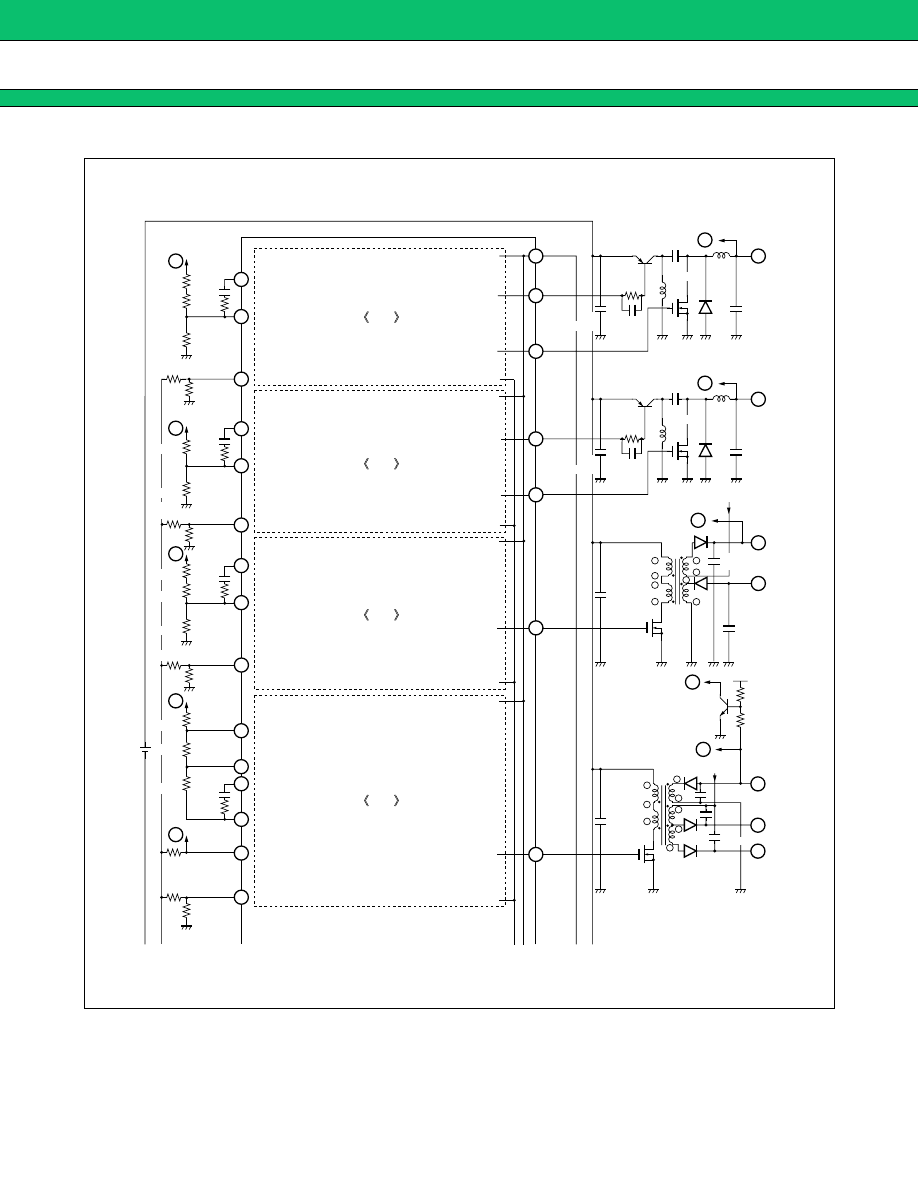
• Block diagram (Expansion 1/2)
PWM
Comp.
1-2
−
+
+
−
+
+
+
−
+
+
−
CH1
Drive
1-1
Drive
1-2
−
+
+
−
+
+
+
−
+
+
−
CH2
Drive
2-1
Drive
2-2
−
+
+
−
+
+
+
−
+
CH3
Drive
3
−
+
+
−
+
+
+
−
+
−
+
CH4
Drive
4
35
34
36
32
31
33
29
28
30
9
10
11
12
13
14
FB1
−
IN1
DTC1
FB2
−
IN2
DTC2
FB3
−
IN3
DTC3
−
IN (A) 4
OUT (A) 4
FB4
−
IN4
−
IN (S) 4
DTC4
42
37
38
39
40
41
43
VCC (O)
OUT1-1
OUT1-2
OUT2-1
OUT2-2
OUT3
OUT4
PWM
Comp.
1-1
VB1
PWM
Comp.
2-2
PWM
Comp.3
PWM
Comp.4
PWM
Comp.
2-1
VB1
Error
Amp.1
SCP
Comp.1
1.25 V
1.0 V
Error
Amp.2
1.25 V
1.0 V
SCP
Comp.2
Error
Amp.3
1.25 V
1.0 V
SCP
Comp.3
1.25 V
1.0 V
SCP
Comp.4
Error
Amp.4
INV
Amp.4
MB3883
8
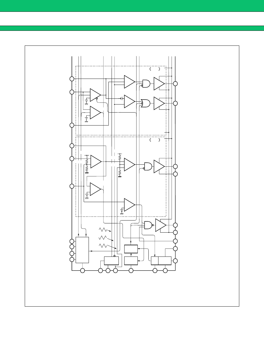
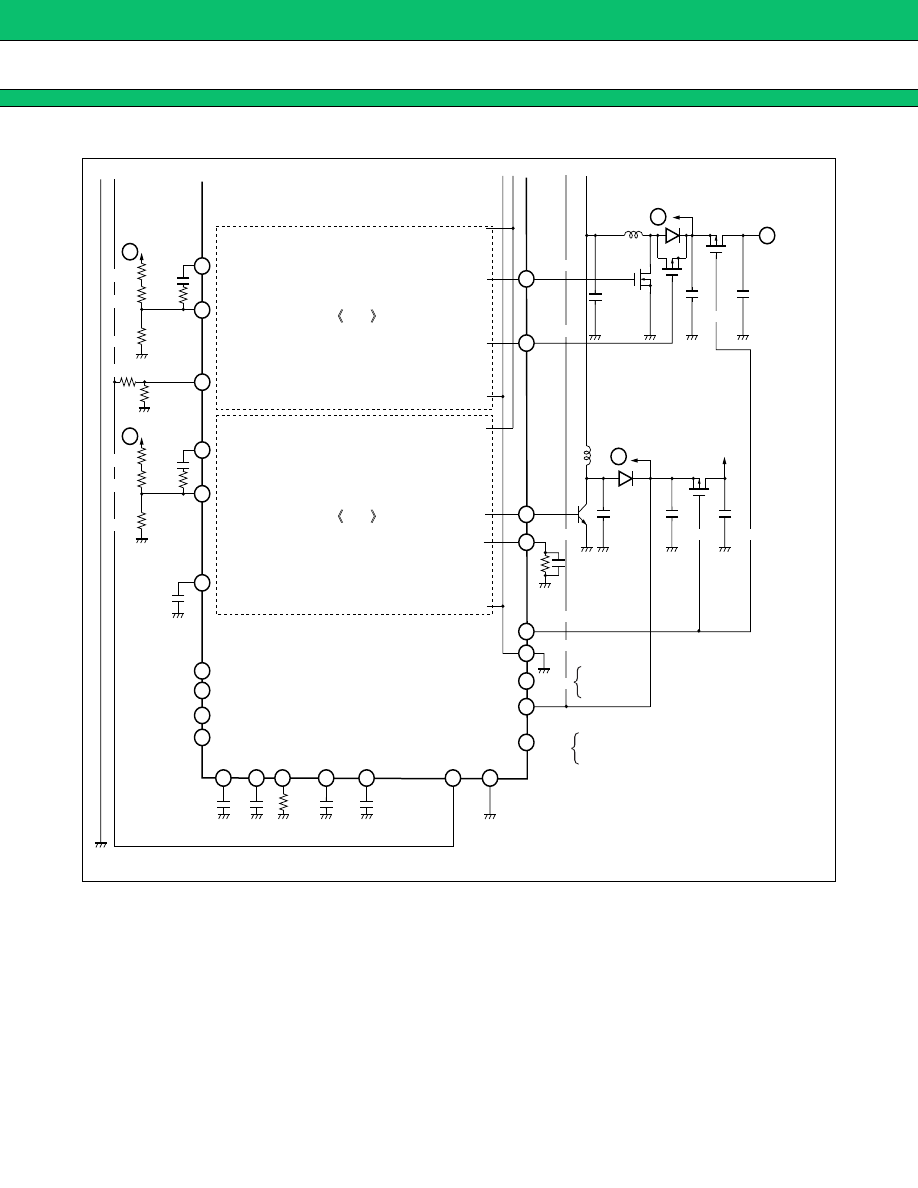
• Block diagram (Expansion 2/2)
PWM
Comp.
5-2
−
+
+
−
+
+
+
−
+
+
−
CH5
CH6
Drive
5-1
Drive
5-2
PWM
Comp.
5-1
VB1
Error
Amp.5
1.25 V
1.0 V
1.26 V
62.5 k
Ω
37 k
Ω
0.9 V
+
−
+
−
+
−
+
−
+
Drive
6
SW
Drive
PWM
Comp.6
Power
Comp.
0.9V
21
CTL1, 2
22
CTL3
23
CTL4
24
CTL5
1 SWOUT
44 GND (O)
2 SWIN
19 VCC
20
17
GND
16
VREF
18
CSCP
26
CT
25
RT
27
VB
15
CS
CTL
3
FB6
4
5
−
IN6
C
+
IN6
7
8
6
FB5
−
IN5
DTC5
45
46
OUT5-1
OUT5-2
47
48
OUT6
RB6
SCP
Comp.5
Error
Amp.6
37.5 k
Ω
(VB : 2 V)
(VB : 2 V)
0.74 V
63 k
Ω
CT1
CT2
CT
1.8 V
−
1.1 V
−
1.8 V
−
1.1 V
−
0.8 V
−
0.3 V
−
CS CTL
Logic
2 V
2.49 V
OSC
SCP
Ref
Power
ON/OFF
CTL
UVLO
(48 Pin)
SCP
Comp.6
H : ON (Power/CH6)
L : OFF (Standby mode)

MB3883
9
■
■
■
■
ABSOLUTE MAXIMUM RATINGS
* : The packages are mounted on the epoxy board (10 cm
×
10 cm).
WARNING: Semiconductor devices can be permanently damaged by application of stress (voltage, current,
temperature, etc.) in excess of absolute maximum ratings. Do not exceed these ratings.
Parameter
Symbol
Condition
Rating
Unit
Min.
Max.
Power supply voltage
V
CC
10
V
I
O
OUT pin
20
mA
Output current
I
O
OUT pin, Duty
≤
5%
200
mA
Output peak current
P
D
Ta
≤
+
25
°
C (LQFP-48P)
860*
mW
Power dissipation
Ta
≤
+
25
°
C (BCC-48P)
710*
mW
Storage temperature
Tstg
−
55
+
125
°
C
MB3883
10
■
■
■
■
RECOMMENDED OPERATING CONDITIONS
WARNING: The recommended operating conditions are required in order to ensure the normal operation of the
semiconductor device. All of the device’s electrical characteristics are warranted when the device is
operated within these ranges.
Always use semiconductor devices within their recommended operating condition ranges. Operation
outside these ranges may adversely affect reliability and could result in device failure.
No warranty is made with respect to uses, operating conditions, or combinations not represented on
the data sheet. Users considering application outside the listed conditions are advised to contact their
FUJITSU representatives beforehand.
Parameter
Symbol
Condition
Value
Unit
Min.
Typ.
Max.
Startup power supply voltage
V
CC
CH6
1.7
9
V
Power supply voltage
V
CC
CH6
2.4
5.0
9
V
CH1 to CH5
3.6
5.0
9
V
Reference voltage output current
I
OR
VREF pin
−
1
0
mA
VB pin output current
I
B
VB pin
−
0.5
0
mA
Input voltage
V
IN
−
IN1 to
−
IN5,
−
IN (A) 4,
−
IN (S) 4 pin
0
V
CC
−
1.8
V
−
IN6 pin
0
V
CC
−
0.9
V
Control input voltage
V
CTL
CTL pin
0
9
V
Output current
I
O
OUT pin (CH1 to CH5)
2
15
mA
OUT pin (CH6)
1
2
15
mA
SWOUT pin
1
4
mA
Output current setting resister
R
B
RB6 pin
2.4
24
51
k
Ω
Oscillator frequency
f
OSC
100
500
1000
kHz
Timing capacitor
C
T
47
100
560
pF
Timing resistor
R
T
8.2
18
100
k
Ω
Soft-start capacitor
C
S
CH1 to CH5
0.027
1.0
µ
F
C
+
IN6
CH6
0.47
1.0
µ
F
Short detection capacitor
C
SCP
0.1
1.0
µ
F
VB pin capacitor
C
VB
0.082
0.18
µ
F
Operating ambient temperature
Ta
−
30
25
85
°
C
MB3883
11
■
■
■
■
ELECTRICAL CHARACTERISTICS
(Ta
=
+
25
°
C, VCC
=
5 V)
*: Standard design value.
(Continued)
Parameter
Symbol
Pin No.
Conditions
Value
Unit
Min.
Typ.
Max.
Reference
voltage
block [REF]
Reference
voltage
V
REF
16
2.46
2.49
2.51
V
Output voltage
temperature
stability
∆
V
REF
/V
REF
16
Ta
=
−
30
°
C to
+
85
°
C
0.5*
%
Input stability
Line
16
VCC
=
3.6 V to 9 V
−
10
10
mV
Load stability
Load
16
VREF
=
0 mA to
−
1 mA
−
10
10
mV
Short-circuit
output current
I
OS
16
VREF
=
2 V
−
20
−
5
−
1
mA
Under voltage
lockout protection
circuit block [U.V.L.O]
CH1 to CH5
Threshold
voltage
V
TH
37
VCC
=
2.6
2.8
3.0
V
Hysteresis
width
V
H
37
0.2
V
Reset voltage
V
RST
37
VCC
=
1.20
1.30
1.40
V
CH6
Threshold
voltage
V
TH
47
VCC
=
1.35
1.5
1.65
V
Soft-start
block
[CS]
Input standby
voltage
V
STB
15
50
100
mV
Charge current
I
CS
15
−
1.4
−
1.0
−
0.6
µ
A
Short circuit
detection block
[SCP]
Threshold
voltage
V
TH
18
0.65
0.70
0.75
V
Input standby
voltage
V
STB
18
50
100
mV
Input latch
voltage
V
I
18
50
100
mV
Input source
current
I
CSCP
18
−
1.4
−
1.0
−
0.6
µ
A
Triangular
wave oscillator
block
[OSC]
Oscillator
frequency
f
OSC
37, 38, 39, 40, 41,
43, 45, 46, 47
CT
=
100 pF, RT
=
18 k
Ω
VB
=
2 V
450
500
550
kHz
Frequency
stability for
voltage
∆
f/fdv
37, 38, 39, 40, 41,
43, 45, 46, 47
VCC
=
4 V to 13 V
1
10
%
Frequency
stability for
temperature
∆
f/fdt
37, 38, 39, 40, 41,
43, 45, 46, 47
Ta
=
−
30
°
C to
+
85
°
C
1*
%
MB3883
12
(Ta
=
+
25
°
C, VCC
=
5 V)
*: Standard design value.
(Continued)
Parameter
Symbol
Pin No.
Conditions
Value
Unit
Min.
Typ.
Max.
Error amplifier block
(CH1 to CH5)
[Error Amp.]
Threshold voltage
V
TH
35, 32, 29, 11, 7 FB
=
1.45 V
1.23
1.25
1.27
V
V
T
temperature
stability
∆
V
T
/V
T
35, 32, 29, 11, 7 Ta
=
−
30
°
C to
+
85
°
C
0.5*
%
Input bias current
I
B
34, 31, 28, 8
−
IN
=
0 V
(CH1 to CH3, CH5)
−
320
−
80
nA
12
−
IN
=
0 V
(CH4)
−
120
−
30
nA
Voltage gain
A
V
35, 32, 29, 11, 7 DC
60
100
dB
Frequency bandwidth
BW
35, 32, 29, 11, 7 A
V
=
0 dB
1.0*
MHz
Output voltage
V
OH
35, 32, 29, 11, 7
2.2
2.4
V
V
OL
35, 32, 29, 11, 7
50
200
mV
Output source current
I
SOURCE
35, 32, 29, 11, 7 FB
=
1.45 V
−
2.0
−
1.0
mA
Output sink current
I
SINK
35, 32, 29, 11, 7 FB
=
1.45 V
70
140
µ
A
Error amplifier bolck
(CH6)
[Error Amp.]
Threshold voltage
V
TH
3
FB
=
0.55 V
1.24
1.26
1.28
V
V
T
temperature
stability
∆
V
T
/V
T
3
Ta
=
−
30
°
C to
+
85
°
C
0.5*
%
Input bias current
I
B
4
−
IN
=
0 V
−
100
−
20
nA
Voltage gain
A
V
3
DC
60
75
dB
Frequency bandwidth
BW
3
A
V
=
0 dB
1.0*
MHz
Output voltage
V
OH
3
1.1
1.3
V
V
OL
3
0
200
mV
Output source current
I
SOURCE
3
FB
=
0.55 V
−
2.0
−
1.0
mA
Output sink current
I
SINK
3
FB
=
0.55 V
60
120
µ
A
Inverting amplifier
bolck (CH4)
[Inv Amp.]
Input offset voltage
V
IO
10
OUT
=
1.25 V
−
10
0
10
mV
Input bias current
I
B
9
−
IN
=
0 V
−
120
−
30
nA
Voltage gain
A
V
10
DC
60
100
dB
Frequency bandwidth
BW
10
A
V
=
0 dB
1.0*
MHz
Output voltage
V
OH
10
2.2
2.4
V
V
OL
10
50
200
mV
Output source current
I
SOURCE
10
OUT
=
1.25 V
−
2.0
−
1.0
mA
Output sink current
I
SINK
10
OUT
=
1.25 V
70
140
µ
A
MB3883
13
(Ta
=
+
25
°
C, VCC
=
5 V)
*: Standard design value.
(Continued)
Parameter
Symbol
Pin No.
Conditions
Value
Unit
Min.
Typ. Max.
Short detection
comparator block
(CH1 to CH5)
[SCP Comp.]
Threshold voltage
V
TH
37, 38, 39, 40,
41, 43, 45, 46
CH1 to CH5
0.97
1.00
1.03
V
Input bias current
I
B
34, 31, 28, 8
−
IN
=
0 V
(CH1 to CH3, CH5)
−
320
−
80
nA
13
−
IN
=
0 V (CH4)
−
200
−
50
nA
Short detection
comparator
block (CH6)
Threshold voltage
V
TH
47
0.8
0.9
1.0
V
PWM Comp. block
(CH1 to CH5)
[PWM Comp.]
Threshold voltage
V
T0
37, 39, 41, 43, 45 Duty cycle
=
0 %
1.0
1.1
V
V
T100
37, 39, 41, 43, 45 Duty cycle
=
100 %
1.8
1.9
V
Input current
I
DTC
36, 33, 30, 14, 6
DTC
=
0.4 V
(CH1 to CH5)
−
1.0
−
0.3
µ
A
PWM Comp.
block(CH6)
[PWM Comp.]
Threshold voltage
V
T0
47
Duty cycle
=
0 %
0.2
0.3
V
V
Tmax
47
Duty cycle
=
Max.
0.74
0.84
V
Maximum duty cycle
Dtr
47
CT
=
100 pF, RT
=
18 k
Ω
,
RB
=
24 k
Ω
70
80
90
%
Output block
(CH1
,
CH2
,
CH5)
[Drive-1(Pch MOS)]
Output source
current
I
SOURCE
37, 39, 45
Duty
≤
5 %, OUT
=
0 V
−
130
mA
Output sink current
I
SINK
37, 39, 45
Duty
≤
5 %, OUT
=
5 V
100
mA
Output ON resistor
R
OH
37, 39, 45
OUT
=
−
15 mA
18
30
Ω
R
OL
37, 39, 45
OUT
=
15 mA
16
25
Ω
Output block
(CH1 to CH5)
[Drive-2(Nch MOS)]
Output source
current
I
SOURCE
38, 40, 41, 43, 46 Duty
≤
5 %, OUT
=
0 V
−
130
mA
Output sink current
I
SINK
38, 40, 41, 43, 46 Duty
≤
5 %, OUT
=
5 V
100
mA
Output ON resistor
R
OH
38, 40, 41, 43, 46 OUT
=
−
15 mA
18
30
Ω
R
OL
38, 40, 41, 43, 46 OUT
=
15 mA
16
25
Ω
Output block
(CH6)
[Drive]
Output source
current
I
SOURCE
47
RB
=
24 k
Ω
, OUT
=
0.7 V
−
2.6
−
2.0
−
1.4
mA
Output sink current
I
SINK
47
Duty
≤
5 %, OUT
=
0.7 V
40
mA
MB3883
14
(Continued)
(Ta
=
+
25
°
C, VCC
=
5 V)
*: Standard design value.
Parameter
Symbol
Pin No.
Conditions
Value
Unit
Min.
Typ.
Max.
Output switch control
block (Drive-1
[SW])
SW input voltage
V
IH
5
SWOUT
=
“L” level
1.5
9
V
V
IL
5
SWOUT
=
“H” level
0
0.5
V
Input current
I
SWIN
5
SWIN
=
5 V
100
200
µ
A
Output source
current
I
SOURCE
1
Duty
≤
5 %,
SWOUT
=
0 V
−
9
mA
Output sink current
I
SINK
1
Duty
≤
5 %,
SWOUT
=
5 V
17
mA
Output ON resistor
R
OH
1
SWOUT
=
−
4 mA
250
400
Ω
R
OL
1
SWOUT
=
4 mA
100
150
Ω
Control block
(CTL, CTL1 to CTL5)
[CTL]
CTL input voltage
V
IH
20, 21, 22,
23, 24
Active mode
1.5
9
V
V
IL
20, 21, 22,
23, 24
Standby mode
0
0.5
V
Input current
I
CTL
20, 21, 22,
23, 24
CTL
=
5 V
100
200
µ
A
General
Standby current
I
CCS
19
CTL
=
0 V
10
µ
A
I
CCS
(
O
) 42
CTL
=
0 V
10
µ
A
Power supply current
I
CC
19, 42
CTL
=
CTL1, 2
=
CTL3
=
CTL4
=
CTL5
=
5 V
6
9
mA
MB3883
15
■
■
■
■
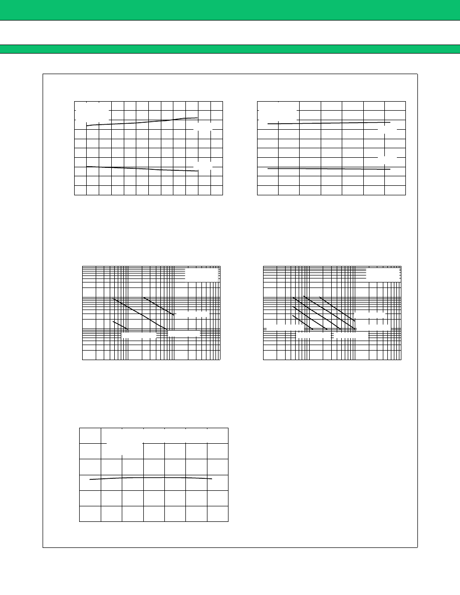
TYPICAL CHARACTERISTICS
(Continued)
10
8
6
4
2
0
0
2
4
6
8
10
Ta
=
+
25
°
C
CTL
=
CTL1, 2
=
CTL3
=
CTL4
=
CTL5
=
5 V
5
4
3
2
1
0
0
2
4
6
8
10
Ta
=
+
25
°
C
CTL
=
CTL1, 2
=
CTL3
=
CTL4
=
CTL5
=
5 V
VREF
=
0 mA
2.56
2.54
2.52
2.5
2.48
2.46
2.44
−
40
−
20
0
20
40
60
80
100
VCC
=
5 V
CTL
=
CTL1, 2
=
CTL3
=
CTL4
=
CTL5
=
5 V
VREF
=
0 mA
5
4
3
2
1
0
0
1
2
3
4
5
Ta
=
+
25
°
C
VCC
=
5 V
VREF
=
0 mA
Ta
=
+
25
°
C
VCC
=
5 V
300
250
200
150
100
50
0
0
2
4
6
8
10
CTL
CTL1, 2
∼
CTL5
Power supply current I
CC
(mA)
Reference voltage V
REF
(V)
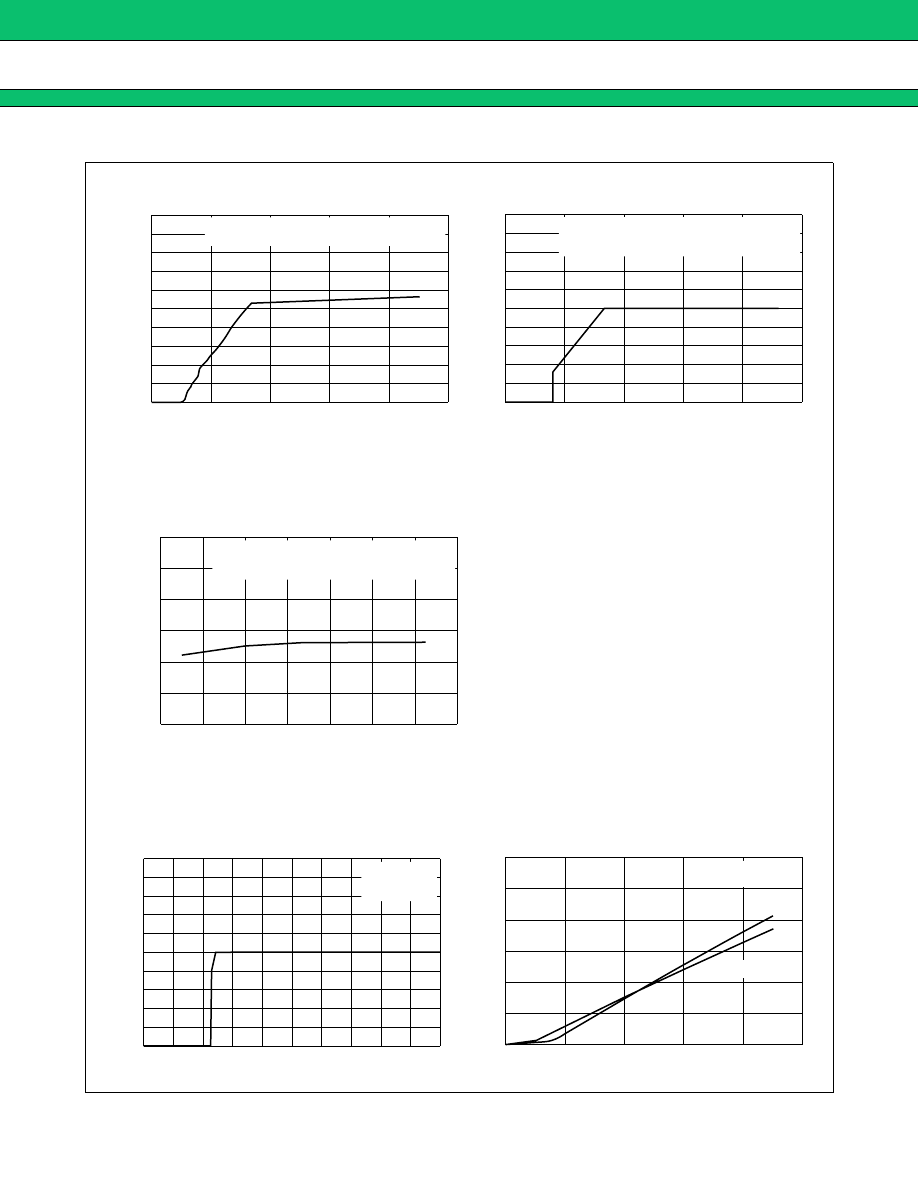
Power supply current vs. power supply voltage
Reference voltage vs. power supply voltage
Power supply voltage V
CC
(V)
Power supply voltage V
CC
(V)
Reference voltage vs. control voltage
Reference voltage V
REF
(V)
Ambient temperature Ta (
°
C)
Reference voltage V
REF
(V)
Reference voltage vs. ambient temperature
Control voltage V
CTL
(V)
Control current I
CTL
(
µ
A)
Control current vs. control voltage
Control voltage V
CTL
(V)
MB3883
16
(Continued)
Ta
=
+
25
°
C
VCC
=
5 V
RT
=
18 k
Ω
1
0.9
0.8
0.7
0.6
0.5
0.4
0.3
0.2
0.1
0
0
200
400
600
800
1000
1200
VCC
=
5 V
RT
=
18 k
Ω
CT
=
100 pF
1
0.9
0.8
0.7
0.6
0.5
0.4
0.3
0.2
0.1
0
−
40
−
20
0
20
40
60
80
100
Ta
=
+
25
°
C
VCC
=
5 V
10000
1000
100
10
10
100
1000
10000
RT
=
100 k
Ω
RT
=
18 k
Ω
RT
=
4.3 k
Ω
Ta
=
+
25
°
C
VCC
=
5 V
10000
1000
100
10
1 k
10 k
100 k
1 M
CT
=
1000 pF
CT
=
100 pF
CT
=
47 pF
CT
=
470 pF CT
=
220 pF
VCC
=
5 V
CTL
=
CTL1, 2
=
CTL3
=
CTL4
=
CTL5
=
5 V
RT
=
18 k
Ω
CT
=
100 pF
560
540
520
500
480
460
440
−
40
−
20
0
20
40
60
80
100
Triangular wave upper and lower limit voltage
vs. ambient temperature
Triangular wave upper and
lower limit voltage V
CT
(V)
Ambient temperature Ta (
°
C)
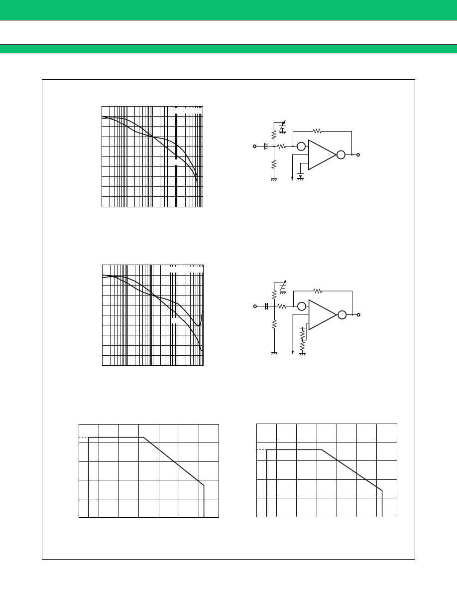
Triangular wave oscillator frequency
vs. timing capacitor
Triangular wave oscillator
frequency f
OSC
(kHz)
Timing capacitor C
T
(pF)
Triangular wave oscillator frequency
vs. timing resistor
Triangular wave oscillator
frequency f
OS
C
(kHz)
Timing resistor R
T
(
Ω
)
Triangular wave oscillator frequency
vs. ambient temperature
Triangular wave oscillator
frequency f
OSC
(kHz)
Ambient temperature Ta (
°
C)
Upper
Lower
Triangular wave upper and
lower limit voltage V
CT
(V
)
Triangular wave upper and lower limit voltage
vs. triangular wave oscillator frequency
Triangular wave oscillator frequency f
OSC
(kHz)
Upper
Lower
MB3883
17
(Continued)
−
− +
+
+
40
20
0
1 k
10 k
100 k
1 M
10 M
−
180
−
90
0
90
180
1
µ
F
−
20
−
40
A
V
φ
Ta
=
+
25
°
C
VCC
=
5 V
240 k
Ω
2.4 k
Ω
10 k
Ω
10 k
Ω
CS CTL Logic
Error Amp.1
1.25 V
IN
OUT
35
34
−
− +
+
+
40
20
0
1 k
10 k
100 k
1 M
10 M
−
180
−
90
0
90
180
1
µ
F
−
20
−
40
A
V
φ
Ta
=
+
25
°
C
VCC
=
5 V
240 k
Ω
2.4 k
Ω
10 k
Ω
10 k
Ω
CS CTL Logic
Error Amp.6
1.26 V
IN
OUT
VB
3
4
1000
800
600
400
200
0
−
40
−
20
0
20
40
60
80
100
860
1000
800
600
400
200
0
−
40
−
20
0
20
40
60
80
100
710
Error amplifier gain and phase vs. frequency (CH1)
Gain A
V
(dB)
Phase
φ
(deg)
Frequency f (Hz)
Error amplifier gain and phase vs. frequency (CH6)
Power dissipation vs. ambient temperature
(LQFP-48P)
Power dissipation P
D
(mW)
Ambient temperature Ta (
°
C)
Gain A
V
(dB)
Phase
φ
(deg)
Frequency f (Hz)
Power dissipation vs. ambient temperature
(BCC-48P)
Power dissipation P
D
(mW)
Ambient temperature Ta (
°
C)

MB3883
18
■
■
■
■
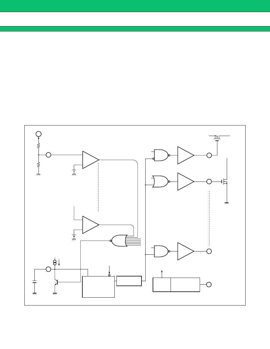
FUNCTIONS
1.
DC-DC Converter Functions
(1) Reference voltage block
The reference voltage circuit generates a temperature-compensated reference voltage (typically := 2.49 V) from
the voltage supplied from the power supply terminal (pin 19). The voltage is used as the reference voltage for
the IC’s internal circuitry.
The reference voltage can supply a load current of up to 1 mA to an external device through the VREF terminal
(pin 16).
(2) Triangular-wave oscillator block
The triangular wave oscillator incorporates a timing capacitor and a timing resistor connected respectively to
the CT terminal (pin 26) and RT terminal (pin 25) to generate triangular oscillation waveform CT (amplitude of
0.3 V to 0.8 V), CT1 (amplitude 1.1 V to 1.8 V in phase with CT), or CT2 (amplitude 1.1 V to 1.8 V in inverse
phase with CT).
CT1 and CT2 are input to the PWM comparator in the IC.
(3) Error amplifier (Error Amp.) block
The error amplifier detects the DC/DC converter output voltage and outputs PWM control signals. It supports
a wide range of in-phase input voltages from 0 V to “V
CC
- 1.8 V” (channels 1 to 5), or 0 V to “Vcc-0.9 V”(channel6)
allowing easy setting from the external power supply.
In addition, an arbitrary loop gain can be set by connecting a feedback resistor and capacitor from the output
pin to inverted input pin of the error amplifier, enabling stable phase compensation to the system.
(4) Inverting amplifier (Inv Amp.) block
The inverting amplifier detects the DC/DC converter output voltage (as a negative voltage) and outputs a control
signal to the error amp.
(5) PWM comparator (PWM Comp.) block
The PWM comparator is a voltage-to-pulse width converter for controlling the output duty depending on the input
voltage.
Channels 1, 2, and 5 main sides,channel 3,4, and 6 : The comparator keeps the output transistor on while the
error amplifier output voltage and DTC voltageremain
higher than the triangular wave voltage.
Channels 1, 2, and 5 synchronous rectification sides : The comparator keeps the output transistor on while the
error amplifier output voltage remain lower than the tri-
angular wave voltage.
(6) Output block
The output block on the main side and on the synchronous rectification side is both in the totem pole configuration,
capable of driving an external P-channel MOS FET (channels 1, 2 main sides, channel 5 synchronous rectification
side), NPN transistor (channel 6), and N-channel MOS FET (channels 3, 4, channel 5 main side, channels 1, 2
synchronous rectification sides).
MB3883
19
2.
Channel Control Function
Channels are turned on and off depending on the voltage levels at the CTL terminal (pin 20), CTL1, 2 terminal
(pin 21), CTL3 terminal (pin 22), CTL4 terminal (pin 23), and CTL5 terminal (pin 24).
Channel On/Off Setting Conditions
×
: Undefined
3.
Protective Functions
(1) Timer-latch short-circuit protection circuit
The short-circuit detection comparator in each channel detects the output voltage level and, if any channel output
voltage falls below the short-circuit detection voltage, the timer circuits is actuated to start charging the external
capacitor C
SCP
connected to the CSCP terminal (pin 18).
When the capacitor voltage reaches about 0.70 V, the circuit is turned off the output transistor and sets the dead
time to 100 %.
To reset the actuated protection circuit, turn the power supply on back. (See “SETTING TIME CONSTANT FOR
TIMER-LATCH SHORT-CIRCUIT PROTECTION CIRCUIT”.)
(2) Undervoltage lockout protection circuit
The transient state or a momentary decrease in supply voltage, which occurs when the power supply is turned
on, may cause the IC to malfunction, resulting in breakdown or degradation of the system. To prevent such
malfunctions, the undervoltage lockout protection circuit detects a decrease in internal reference voltage with
respect to the power supply voltage, turns off the output transistor, and sets the dead time to 100% while holding
the CSCP terminal (pin 18) at the “L” level.
The circuit restores the output transistor to normal when the supply voltage reaches the threshold voltage of the
undervoltage lockout protection circuit.
(3) Output switch control circuit
When the power is turned on, this circuit prevents reactive current flow to external step-up circuits on CH5 and
CH6. When the SWIN terminal (pin 2) is a state at “H” level after releasing UVLO and the C+IN6 terminal (pin5)
voltage goes above 0.9 V (Typ.), the SWOUT terminal (pin 1) becomes “L” level. External P-ch MOS FET is
turned on at this time and the output voltage is generated.
Voltage level at CTL pin
Channel on/off state
CTL
CTL1, 2
CTL3
CTL4
CTL5
Power/CH6
CH1, CH2
CH3
CH4
CH5
L
×
×
×
×
OFF (Standby state)
H
L
L
L
L
ON
OFF
OFF
OFF
OFF
H
ON
H
L
ON
OFF
H
ON
H
L
L
ON
OFF
OFF
H
ON
H
L
ON
OFF
H
ON
H
L
L
L
ON
OFF
OFF
OFF
H
ON
H
L
ON
OFF
H
ON
H
L
L
ON
OFF
OFF
H
ON
H
L
ON
OFF
H
ON
MB3883
20
4.
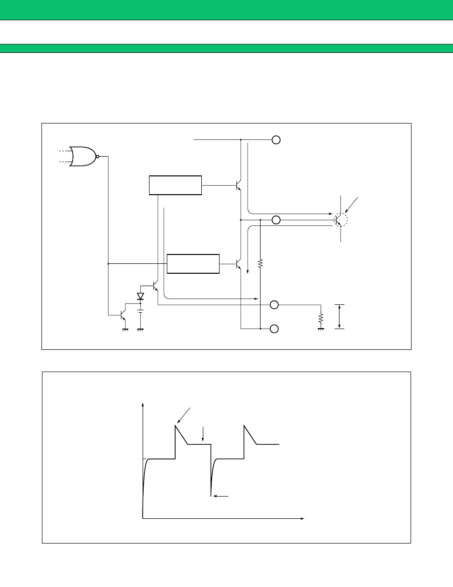
Soft Start Operation
1. Description
• When the CTL, CTL1,2, CTL3, CTL4, and CTL5 terminals are driven high (“H” level) at the same time
The capacitor (C+IN6) connected to the C+IN6 terminal (pin 5) starts charging. When the C+IN6 terminal voltage
falls below 0.9 V (Typ.), the capacitor (Cs) connected to the CS terminal (pin 15) starts charging and the error
amp. provides a soft start by comparing the CH1 to CH5 output voltage to the voltage at the CS terminal.
t
0.9 V
2 V
2.49 V
1.25 V
(1) to (2)
:
CH6
soft start interval
(3) to (4)
:
CH1 to CH5
soft start interval
Input
CTL (pin 20)
CTL1, 2 (pin 21)
CTL3 (pin 22)
CTL4 (pin 23)
CTL5 (pin 24)
Output
VB (pin 27)
C
+
IN6 (pin 5)
CH6 output voltage
Vo6
VREF (pin 16)
CS (pin15)
CH1 to CH5 output
voltage Vo1 to Vo5
(1)
(3) (2)
(4)
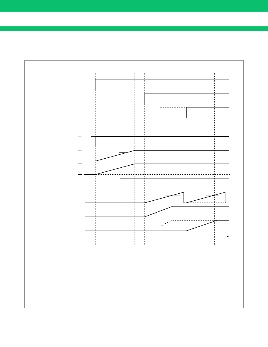
MB3883
21
• After a CH6 soft start, when the CTL1, 2, CTL3, CTL4, and CTL5 terminals are driven high
The capacitor (Cs) connected to the CS terminal (pin 15) starts charging and the error amp provides a soft start
by comparing the CH1 to CH5 output voltage to the voltage at the CS terminal.
Note : Each of the terminals CTL1,2, CTL3, CTL4, and CTL5 can be switched on or off independently. When any of
these CTL terminals is switched on, a soft start operation is provided as shown in the above timing chart.
t
1.25 V
1.25 V
0.9 V
2 V
2.49 V
Input
CTL ( pin 20)
Output
VB ( pin 27)
C
+
IN6 ( pin 5)
CH6 output voltage
Vo6
VREF ( pin 16)
CS ( pin 15)
CH1 to CH3 output
voltage Vo1 to Vo3
(1)
(3) (2)
(4)
CH4, CH5 output
voltage Vo4, Vo5
CTL1, 2 ( pin 21)
CTL3 ( pin 22)
CTL4 ( pin 23)
CTL5 ( pin 24)
(5)
(6)
(7)
(7)’
(6)’
(1) to (2)
: CH6 soft start interval
(3)
: VREF Output start
(4) to (5)
: CH1 to CH3 soft start interval
(6) to (7)
: CH4, CH5 soft start interval
(6)’ to (7)’
: CH4 (CH5) soft start interval (waveform) as CTL4 (CTL5) go “H”
from “L” during CH1 to CH3 soft start interval
MB3883
22
2. Soft Start Settings
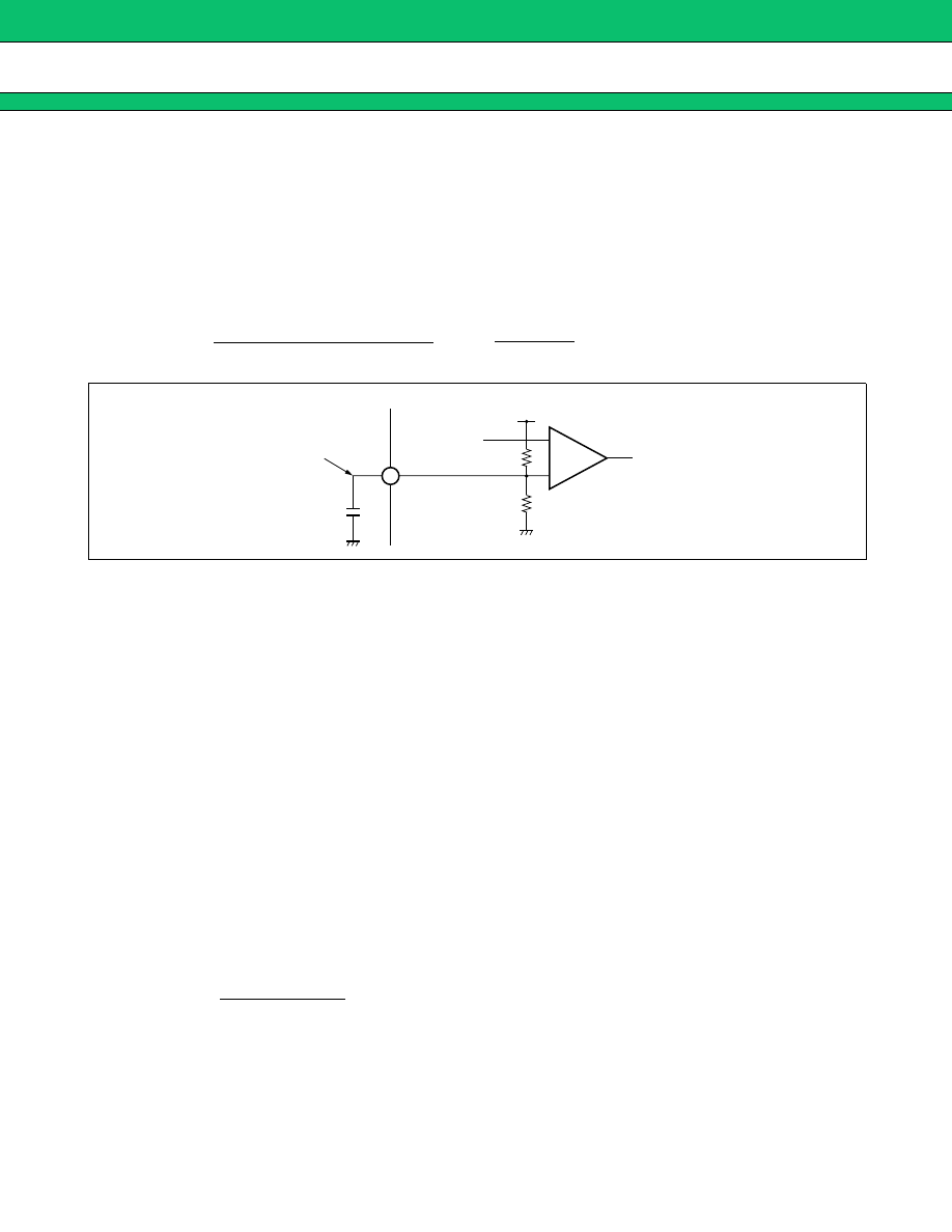
• CH6 soft start time
The soft start operation is determined by the capacitor (C+IN6) connected to the C+IN6 terminal (pin 5). The
soft start time depends on the input voltage and load current.
CH6 soft start time
CH6 soft start equivalent circuit
Example: The soft start time until CH6 output voltage reaches 95% of the set voltage is determined as follows:
ts (s) := 0.07
×
C
+
IN6
(
µ
F)
• CH1 to CH5 soft start time
CH1 to CH5 soft start time
ts (s) := 1.25
×
C
S
(
µ
F)
Note : The short-circuit detection function remains working during soft start operation on channels 1 through 5.
■
■
■
■
SETTING THE TRIANGULAR OSCILLATOR FREQUENCY
The triangular oscillator frequency is determined by the timing capacitor (C
T
) connected to the CT terminal (pin
26), and the timing resistor (R
T
) connected to the RT terminal (pin 25).
Triangular oscillator frequency
ts (s)
=
−
C
+
IN6
(F)
×
37.5 (k
Ω
)
×
62.5 (k
Ω
)
100 (k
Ω
)
V
C
+
IN6
(V)
1.26 (V)
(
)
ln
1
−
−
+
C
+
IN6
V
C
+
IN6
C
+
IN6
(37.5 k
Ω
)
(62.5 k
Ω
)
Error
Amp.6
(1.26 V)
(VB : 2 V)
5
f
OSC
(kHz) :=
900000
C
T
(pF)
•
R
T
(k
Ω
)
MB3883
23
■
■
■
■
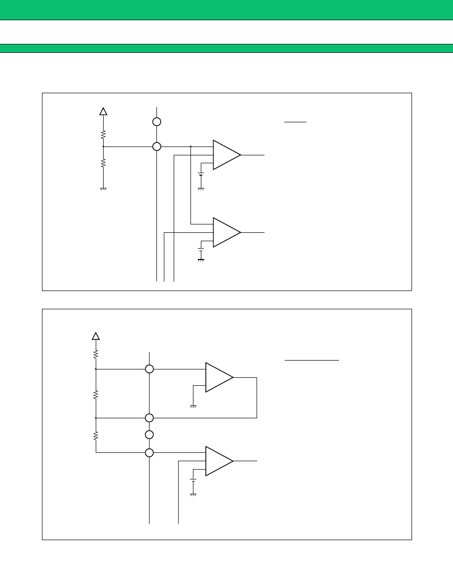
SETTING THE OUTPUT VOLTAGE
• CH1 to CH3, CH5
• CH4
−
+
+
−
+
+
R2
R1
−
IN1
1.25 V
1.25 V
V
O
=
(R1
+
R2 )
1.0 V
Error
Amp.1
SCP
Comp.1
FB1
V
O
R2
35
34
−
+
−
+
+
R2
R1
V
−
IN (A) 4
−
V
OUT (A) 4
V
O
=
R1
1.25 V
INV
Amp.4
Error
Amp.4
−
IN (A) 4
OUT (A) 4
FB4
−
IN4
V
O
R3
R2
V
OUT (A) 4
=
V
−
IN4
[
]
9
10
12
11
MB3883
24
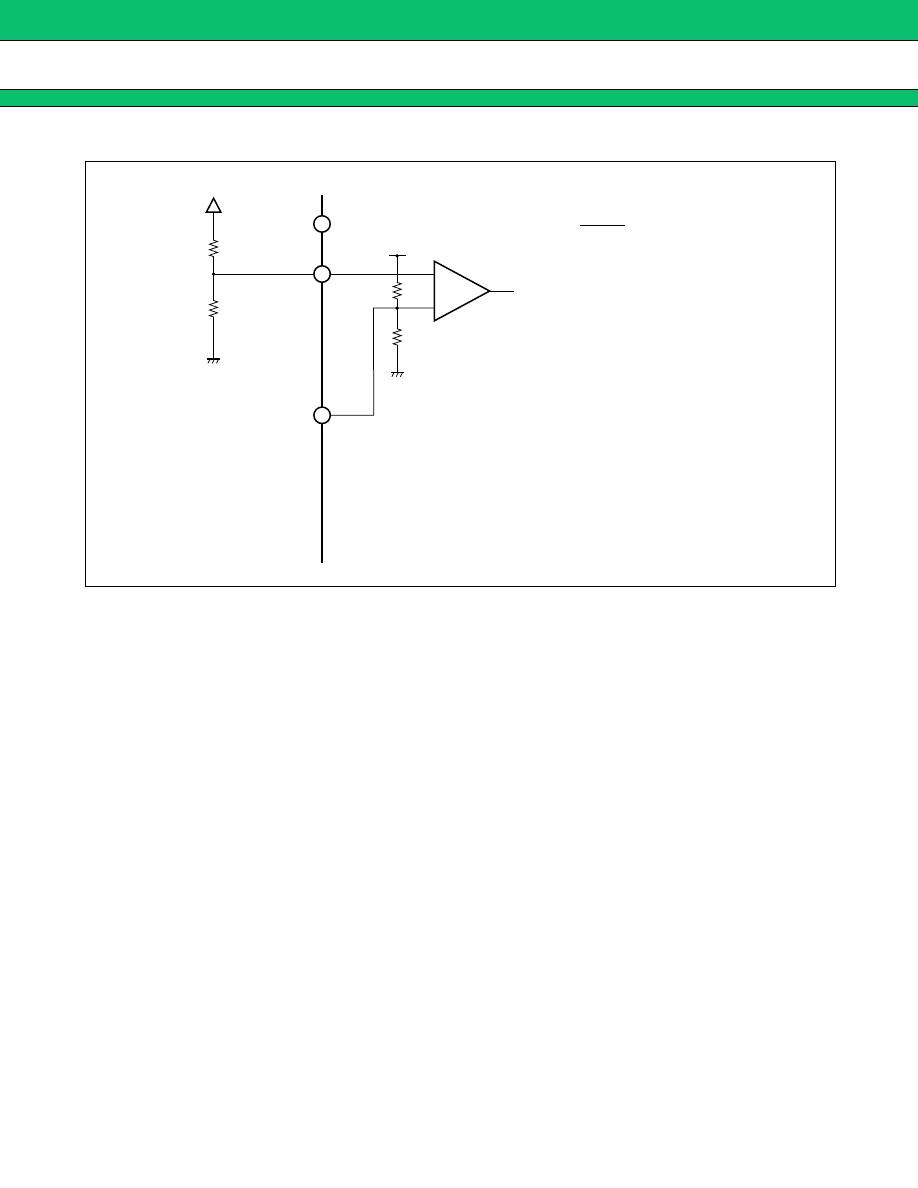
• CH6
−
+
37.5 k
Ω
62.5 k
Ω
1.26 V
Error
Amp.6
(VB : 2 V)
R1
FB6
1.26 V
V
O
=
(R1
+
R2)
−
IN6
C
+
IN6
V
O
R2
R2
3
4
5
MB3883
25
■
■
■
■
SETTING THE OUTPUT CURRENT
The output circuit (drive 6) is structured as illustrated below (in the output circuit diagram). As found in “Output
Current Waveform” below, the source current value of the output current waveform has a constant current setting.
Note that the source current is set by the following equation:
• Output source current
=
(VB
/
RB)
×
80 (A)
In the output circuit diagram
Output current waveform
0.6 V
VCC (O)
I
80 I
70 k
Ω
RB6
R
B
V
B
GND (O)
×
33
×
33
OUT6
47
42
48
44
Source current
Sink current
Output source
current
Output sink
current
External NPN transistor
0
t
Output source current (Peak)
Output source
current
Output sink current (Peak)
Output current
MB3883
26
■
■
■
■
SETTING
TIME
CONSTANT FOR TIMER-LATCH SHORT-CIRCUIT PROTECTION CIRCUIT
The short detection comparator (SCP comparator) in each channel monitors the output voltage.
While the switching regulator load conditions are stable on all channels, the LOG_SCP output remains at “H”
level, transistor Q1 is turned on, and the CSCP terminal (pin 18) is held at “L” level.
If the load condition on a channel changes rapidly due to a short of the load, causing the output voltage to drop,
the output of the short detection comparator on that channel goes to “H” level. This causes transistor Q1 to be
turned off and the external short protection capacitor C
SCP
connected to the CSCP terminal to be charged at 1.0
µ
A.
Short detection time (t
PE
)
t
PE
(s) := 0.70
×
C
SCP
(
µ
F)
When the capacitor C
SCP
is charged to the threshold voltage (VTH := 0.70 V), the latch is set and the external
FET is turned off (dead time is set to 100%). At this point, the latch input is closed and the CSCP terminal is
held at “L” level.
Timer-latch short circuit protection circuit
−
+
A
R1
R2
−
IN1
1.0 V
SCP
Comp.1
−
+
0.9 V
SCP
Comp.6
OUT1
−
1
Drive
1
−
1
OUT1
−
2
Drive
1
−
2
OUT6
CTL
Drive
6
bias
bias
Ref
Power
ON/OFF CTL
S
R
UVLO
Q1
C
SCP
CSCP
1
µ
A
LOG_SCP
34
18
20
47
38
37
External FET
Timer-latch short
protection circuit
MB3883
27
■
■
■
■
TREATMENT WITHOUT USING CSCP
When not using the timer-latch short protection circuit, connect the CSCP terminal (pin 18) to GND with the
shortest distance.
Treatment without using CSCP
■
■
■
■
OPERATING WITHOUT THE SOFT START FUNCTION
To disable the CH1 to CH5 soft start function, leave the CS terminal (pin 15) open.
To disable the CH6 soft start function, leave the C+IN6 terminal (pin 5) open.
When no soft start time is set
18
CSCP
15
CS
5
C
+
IN6
“Open”
“Open”
MB3883
28
■
■
■
■
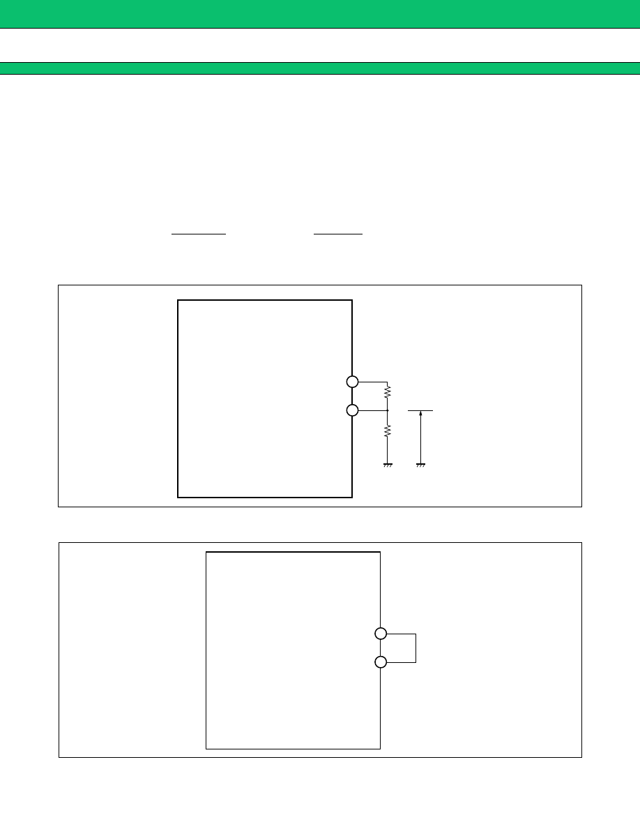
SETTING THE DEAD TIME
When the device is set for step-up inverted output based on the step-up or step-up/down Zeta method or flyback
method, the FB pin voltage may reach and exceed the rectangular wave voltage due to load fluctuation. If this
is the case, the output transistor is fixed to a full-ON state (ON duty = 100 %). To prevent this, set the maximum
duty of the output transistor. To set it, set the voltage at the DTC1 terminal (pin 36) by applying a resistive voltage
divider to the VREF voltage as shown below.
When the voltage at the DTC1 terminal (pin 36) is higher than the triangular wave voltage (CT1), the output
transistor is turned on. The maximum duty calculation formula assuming that triangular wave amplitude := 0.7
V and triangular wave minimum voltage := 1.1 V is given below. (Same to other channels.)
When the DTC1 terminal is not used, connect it directly to the VREF terminal (pin 16) as shown below (when
no dead time is set). (Same to other channels.)
When using DTC to set dead time
(Same to other channels.)
( CH1)
When no dead time is set
( Same to other channels.)
( CH 1)
DUTY (ON) max :=
Vdt
−
1.1 V
0.7 V
×
100 (%) , Vdt
=
Rb
Ra
+
Rb
×
VREF
16
36
VREF
DTC1
Ra
Rb
Vdt
16
36
VREF
DTC1
MB3883
29
■
■
■
■
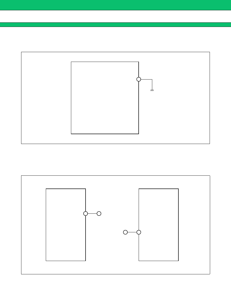
TREATMENT WITHOUT USING CH4 INV Amp.
When not using the CH4 INV Amp., connect the -IN(A)4 terminal (pin 9) to the OUT(A)4 terminal (pin 10) with
the shortest distance.
Treatment without using CH4 INV Amp.
9
10
−
IN(A)4
OUT(A)4
MB3883
30
■
■
■
■
APPLICATION EXAMPLE
F
Q8
Q10
Vo5
(5.0 V)
(100 mA)
L5
15
µ
H
L6
22
µ
H
C13
2.2
µ
F
C21
2.2
µ
F
C30
0.1
µ
F
C31
0.1
µ
F
R40
18 k
Ω
C32
100 pF
C33
0.1
µ
F
G
R11
1 k
Ω
C28
0.1
µ
F
C29
0.33
µ
F
R37
15 k
Ω
R38
30 k
Ω
F
R36
47 k
Ω
R10
1 k
Ω
C27
0.1
µ
F
R32
15 k
Ω
R33
30 k
Ω
R35
24 k
Ω
CH5
CH6
21
CTL1, 2
22
CTL3
23
CTL4
24
CTL5
1
SWOUT
44
GND (O)
2 SWIN
19
VCC
(5.0 V)
20
17
GND
16
VREF
18
CSCP
26
CT
25
RT
27
VB
15
CS
CTL
3
FB6
4
5
−
IN6
C
+
IN6
7
8
6
FB5
−
IN5
DTC5
45
46
OUT5-1
OUT5-2
47
48
OUT6
RB6
(48 Pin)
G
Q12
D9
Vo6
(5.0 V)
C22
2.2
µ
F
C16
56 pF
R5
20 k
Ω
C14
4.7
µ
F
C15
2.2
µ
F
C12
4.7
µ
F
Q11
E
D
Q6
Q7
D5
D6
D7
<LCD>
Vo4-3
(
−
15 V)
(4 mA)
Vo6
(5.0 V)
Vo4-1
(13.5 V)
(2.7 mA)
Vo4-2
(6.5 V)
(6 mA)
C8
1
µ
F
C7
1
µ
F
C20
2.2
µ
F
4
5
6
7
8
3
2
1
C
Q5
VREF
D4
D3
<CCD>
Vo3-1
(15 V)
(12 mA)
Vo6
(5.0 V)
Vo3-2
(
−
7.5 V)
(2.5 mA)
C6
1
µ
F
C19
2.2
µ
F
R3
18 k
Ω
R4
27 k
Ω
CH1
CH2
CH3
CH4
35
A
34
36
FB1
−
IN1
DTC1
FB2
−
IN2
DTC2
FB3
−
IN3
DTC3
−
IN (A) 4
OUT (A) 4
FB4
−
IN4
−
IN (S) 4
DTC4
42
A
38
41
43
VCC (O)
OUT1-1
OUT1-2
OUT2-2
OUT3
OUT4
R12
2.7 k
Ω
R13
22 k
Ω
R14
15 k
Ω
R15
24 k
Ω
R16
47 k
Ω
R20
47 k
Ω
R6
1 k
Ω
C23
0.1
µ
F
C
R29
47 k
Ω
R30
24 k
Ω
R25
47 k
Ω
R8
1 k
Ω
C25
0.1
µ
F
E
D
R31
47 k
Ω
R9
1 k
Ω
C26
0.1
µ
F
B
R7
1 k
Ω
C24
0.1
µ
F
32
31
33
29
28
30
9
10
11
12
13
14
R17
15 k
Ω
R19
24 k
Ω
R21
15 k
Ω
R22
150 k
Ω
R24
24 k
Ω
R26
120 k
Ω
R27
10 k
Ω
R28
10 k
Ω
37
Q1
Q3
D1
Vo1
(3.3 V)
(250 mA)
C1
4.7
µ
F
L2
22
µ
H
C2
4.7
µ
F
L1
15
µ
H
R1
150
Ω
C10
3300 pF
B
Q2
Q4
D2
Vo2
(2.5 V)
(150 mA)
C3
4.7
µ
F
L4
22
µ
H
C4
4.7
µ
F
L3
22
µ
H
R2
300
Ω
C11
2700 pF
39
OUT2-1
40
C5
1
µ
F
4
5
6
7
8
3
2
1
C9
1
µ
F
V
IN
(1.8 V ~
5.0 V)
C18
2.2
µ
F
C17
2.2
µ
F
D8
R18
15 k
Ω
R23
15 k
Ω
R34
15 k
Ω
R39
15 k
Ω
Q9
H:
L:
SWOUT = L
SWOUT = H
H : ON (Power/CH6)
L : OFF (Standby mode)
MB3883
31
• Application example (Expansion1/2)
E
D
Q6
Q7
D5
D6
D7
<LCD>
Vo4-3
(
−
15 V)
(4 mA)
Vo6
(5.0 V)
Vo4-1
(13.5 V)
(2.7 mA)
Vo4-2
(6.5 V)
(6 mA)
C8
1
µ
F
C7
1
µ
F
C20
2.2
µ
F
4
5
6
7
8
3
2
1
C
Q5
VREF
D4
D3
<CCD>
Vo3-1
(15 V)
(12 mA)
Vo6
(5.0 V)
Vo3-2
(
−
7.5 V)
(2.5 mA)
C6
1
µ
F
C19
2.2
µ
F
R3
18 k
Ω
R4
27 k
Ω
CH1
CH2
CH3
CH4
35
A
34
36
FB1
−
IN1
DTC1
FB2
−
IN2
DTC2
FB3
−
IN3
DTC3
−
IN (A) 4
OUT (A) 4
FB4
−
IN4
−
IN (S) 4
DTC4
42
A
38
41
43
VCC (O)
OUT1-1
OUT1-2
OUT2-2
OUT3
OUT4
R12
2.7 k
Ω
R13
22 k
Ω
R14
15 k
Ω
R15
24 k
Ω
R16
47 k
Ω
R20
47 k
Ω
R6
1 k
Ω
C23
0.1
µ
F
C
R29
47 k
Ω
R30
24 k
Ω
R25
47 k
Ω
R8
1 k
Ω
C25
0.1
µ
F
E
D
R31
47 k
Ω
R9
1 k
Ω
C26
0.1
µ
F
B
R7
1 k
Ω
C24
0.1
µ
F
32
31
33
29
28
30
9
10
11
12
13
14
R17
15 k
Ω
R19
24 k
Ω
R21
15 k
Ω
R22
150 k
Ω
R24
24 k
Ω
R26
120 k
Ω
R27
10 k
Ω
R28
10 k
Ω
37
Q1
Q3
D1
Vo1
(3.3 V)
(250 mA)
C1
4.7
µ
F
L2
22
µ
H
C2
4.7
µ
F
L1
15
µ
H
R1
150
Ω
C10
3300 pF
B
Q2
Q4
D2
Vo2
(2.5 V)
(150 mA)
C3
4.7
µ
F
L4
22
µ
H
C4
4.7
µ
F
L3
22
µ
H
R2
300
Ω
C11
2700 pF
39
OUT2-1
40
C5
1
µ
F
4
5
6
7
8
3
2
1
C9
1
µ
F
V
IN
(1.8 V ~
5.0 V)
R18
15 k
Ω
R23
15 k
Ω
C17
2.2
µ
F
C18
2.2
µ
F
MB3883
32
• Application example (Expansion 2/2)
F
Q8
Q10
Vo5
(5.0 V)
(100 mA)
L5
15
µ
H
L6
22
µ
H
C13
2.2
µ
F
C21
2.2
µ
F
C30
0.1
µ
F
C31
0.1
µ
F
R40
18 k
Ω
C32
100 pF
C33
0.1
µ
F
G
R11
1 k
Ω
C28
0.1
µ
F
C29
0.33
µ
F
R37
15 k
Ω
R38
30 k
Ω
F
R36
47 k
Ω
R10
1 k
Ω
C27
0.1
µ
F
R32
15 k
Ω
R33
30 k
Ω
R35
24 k
Ω
CH5
CH6
21
CTL1, 2
22
CTL3
23
CTL4
24
CTL5
1
SWOUT
44
GND (O)
2 SWIN
19
VCC
(5.0 V)
20
17
GND
16
VREF
18
CSCP
26
CT
25
RT
27
VB
15
CS
CTL
3
FB6
4
5
−
IN6
C
+
IN6
7
8
6
FB5
−
IN5
DTC5
45
46
OUT5-1
OUT5-2
47
48
OUT6
RB6
(48 Pin)
G
Q12
D9
Vo6
(5.0 V)
C22
2.2
µ
F
C16
56 pF
R5
20 k
Ω
C14
4.7
µ
F
C15
2.2
µ
F
C12
4.7
µ
F
Q11
D8
R34
15 k
Ω
R39
15 k
Ω
Q9
H:
L:
SWOUT = L
SWOUT = H
H : ON (Power/CH6)
L : OFF (Standby mode)

MB3883
33
■
■
■
■
PARTS LIST
Note : SANYO : SANYO Electric Co., Ltd.
Fairchild : Fairchild Semiconductor Corporation
TDK : TDK Corporation
COMPONENT
ITEM
SPECIFICATION
VENDOR
PARTS NO.
Q1, Q2
Q3 to Q6, Q8
Q9, Q10, Q12
Q7, Q11
PNP Tr
FET
FET
NPN Tr
VCEO
=
−
12 V
VDSS
=
30 V
VDSS
=
−
20 V
VCEO
=
15 V
SANYO
Fairchild
SANYO
SANYO
CPH3106
NDS355AN
CPH3303
CPH3206
D1, D2, D8, D9
D3 to D7
Diode
Diode
VF
=
0.40 V (Max.) , IF
=
1 A
VF
=
0.55 V (Max.) , IF
=
500 mA
SANYO
SANYO
SBS004
SB05-05CP
L1, L5
L2 to L6
Coil
Coil
15
µ
H
22
µ
H
1 A, 74.5 m
Ω
0.77 A, 104 m
Ω
TDK
TDK
SLF6028T-150M1R0
SLF6028T-220MR77
C1 to C4
C5 to C9
C10
C11
C12, C14
C13, C15
C16
C17 to C22
C23 to C28
C29
C30, C31, C33
Ceramics Condensor
Ceramics Condensor
Ceramics Condensor
Ceramics Condensor
Ceramics Condensor
Ceramics Condensor
Ceramics Condensor
Ceramics Condensor
Ceramics Condensor
Ceramics Condensor
Ceramics Condensor
4.7
µ
F
1
µ
F
3300 pF
2700 pF
4.7
µ
F
2.2
µ
F
56 pF
2.2
µ
F
0.1
µ
F
0.33
µ
F
0.1
µ
F
10 V
25 V
50 V
50 V
10 V
16 V
50 V
16 V
16 V
10 V
16 V
R1
R2
R3
R4
R5
R8 to R11
R12
R13
R14
R15, R19, R24
R16, R20, R25
R17, R18, R21
R22
R23, R39
R26
R27, R28
R29, R31, R36
R30, R35
R32, R34, 37
R33, R38
R40
Resistor
Resistor
Resistor
Resistor
Resistor
Resistor
Resistor
Resistor
Resistor
Resistor
Resistor
Resistor
Resistor
Resistor
Resistor
Resistor
Resistor
Resistor
Resistor
Resistor
Resistor
150
Ω
300
Ω
18 k
Ω
27 k
Ω
20 k
Ω
1 k
Ω
2.7 k
Ω
22 k
Ω
15 k
Ω
24 k
Ω
47 k
Ω
15 k
Ω
150 k
Ω
15 k
Ω
120 k
Ω
10 k
Ω
47 k
Ω
24 k
Ω
15 k
Ω
30 k
Ω
18 k
Ω
1/16 W
1/16 W
1/16 W
1/16 W
1/16 W
1/16 W
1/16 W
1/16 W
1/16 W
1/16 W
1/16 W
1/16 W
1/16 W
1/16 W
1/16 W
1/16 W
1/16 W
1/16 W
1/16 W
1/16 W
1/16 W
MB3883
34
■
■
■
■
REFERENCE DATA
(Continued)
A
Q1
IL
Q3
Vo1
×
IL
×
100
Vin
×
Iin
D1
Vo1
(3.3 V)
C1
4.7
µ
F
L2
22
µ
H
L1
10
µ
H
R1
82
Ω
C10
3300 pF
C17
2.2
µ
F
Vin
Iin
C2
4.7
µ
F
η
(%)
=
90
88
86
84
82
80
78
76
74
72
70
0
50
100
150
200
250
300
350
400
450
500
Vin = 2.5 V
Vin = 3 V
Vin = 3.6 V
Vin = 4.2 V
B
Q2
IL
Q4
Vo2
×
IL
×
100
Vin
×
Iin
D2
Vo2
(2.5 V)
C3
4.7
µ
F
L4
22
µ
H
L3
15
µ
H
R2
110
Ω
C11
3300 pF
C18
2.2
µ
F
Vin
Iin
C4
4.7
µ
F
η
(%)
=
90
88
86
84
82
80
78
76
74
72
70
0
50
100
150
200
250
300
350
400
450
500
Vin = 2.5 V
Vin = 3 V
Vin = 3.6 V
Vin = 4.2 V
To OUT1-1
To OUT1-2
Ta
=
+
25
°
C
3.3 V output
VCC
=
VCC(O)
=
5 V
Conversion efficiency
η
(%)
Load current IL (mA)
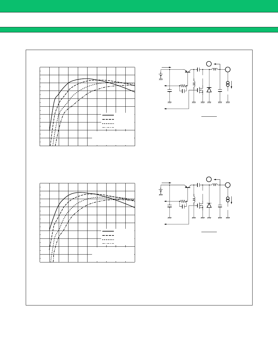
Conversion efficiency vs. load current
(CH1 : Zeta method with synchronous rectification)
To OUT2-1
To OUT2-2
Ta
=
+
25
°
C
2.5 V output
VCC
=
VCC(O)
=
5 V
Conversion efficiency
η
(%)
Load current IL (mA)
Conversion efficiency vs. load current
(CH2 : Zeta method with synchronous rectification)
Note : The above application uses a constant of
Vin=2.5 V, with settings made at maximum load.
MB3883
35
(Continued)
IL
Vin
Iin
Vo5
×
IL
×
100
Vin
×
Iin
η
(%)
=
F
Q8
Q10
Vo5
(5.0 V)
L5
10
µ
H
C21
2.2
µ
F
C12
4.7
µ
F
Q9
D8
C13
2.2
µ
F
100
99
98
97
96
95
94
93
92
91
90
0
50
100
150
200
250
300
Vin = 2.5 V
Vin = 3 V
Vin = 3.6 V
Vin = 4.2 V
To OUT5-1
To OUT5-2
Ta
=
+
25
°
C
5 V output
VCC
=
VCC(O)
=
5 V
Conversion efficiency
η
(%)
Load current IL (mA)
Conversion efficiency vs. load current
(CH5 : Up conversion method with synchronous rectification)
To SWOUT
Note : The above application uses a constant of
Vin=2.5V, with settings made at maximum load.
MB3883
36
■
■
■
■
USAGE PRECAUTION
• Printed circuit board ground lines should be set up with consideration for common impedance.
• Take appropriate static electricity measures.
• Containers for semiconductor materials should have anti-static protection or be made of conductive material.
• After mounting, printed circuit boards should be stored and shipped in conductive bags or containers.
• Work platforms, tools, and instruments should be properly grounded.
• Working personnel should be grounded with resistance of 250 k
Ω
to 1 M
Ω
between body and ground.
• Do not apply negative voltages.
The use of negative voltages below –0.3 V may create parasitic transistors on LSI lines, which can cause
abnormal operation.
■
■
■
■
ORDERING INFORMATION
Part number
Package
Remarks
MB3883PFV
48-pin plastic LQFP
(FPT-48P-M05)
MB3883PV
48-pad plastic BCC
(LCC-48P-M02)
MB3883
37
■
■
■
■
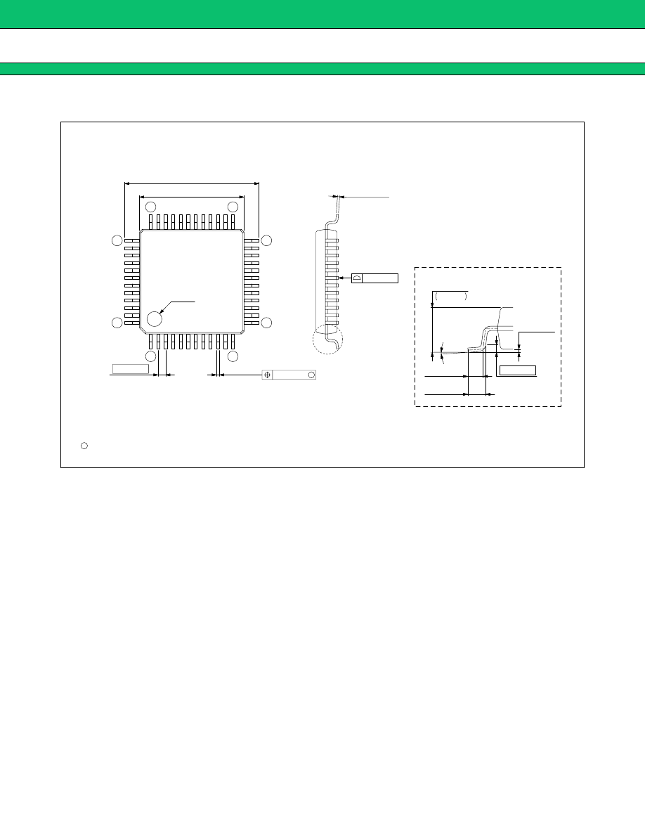
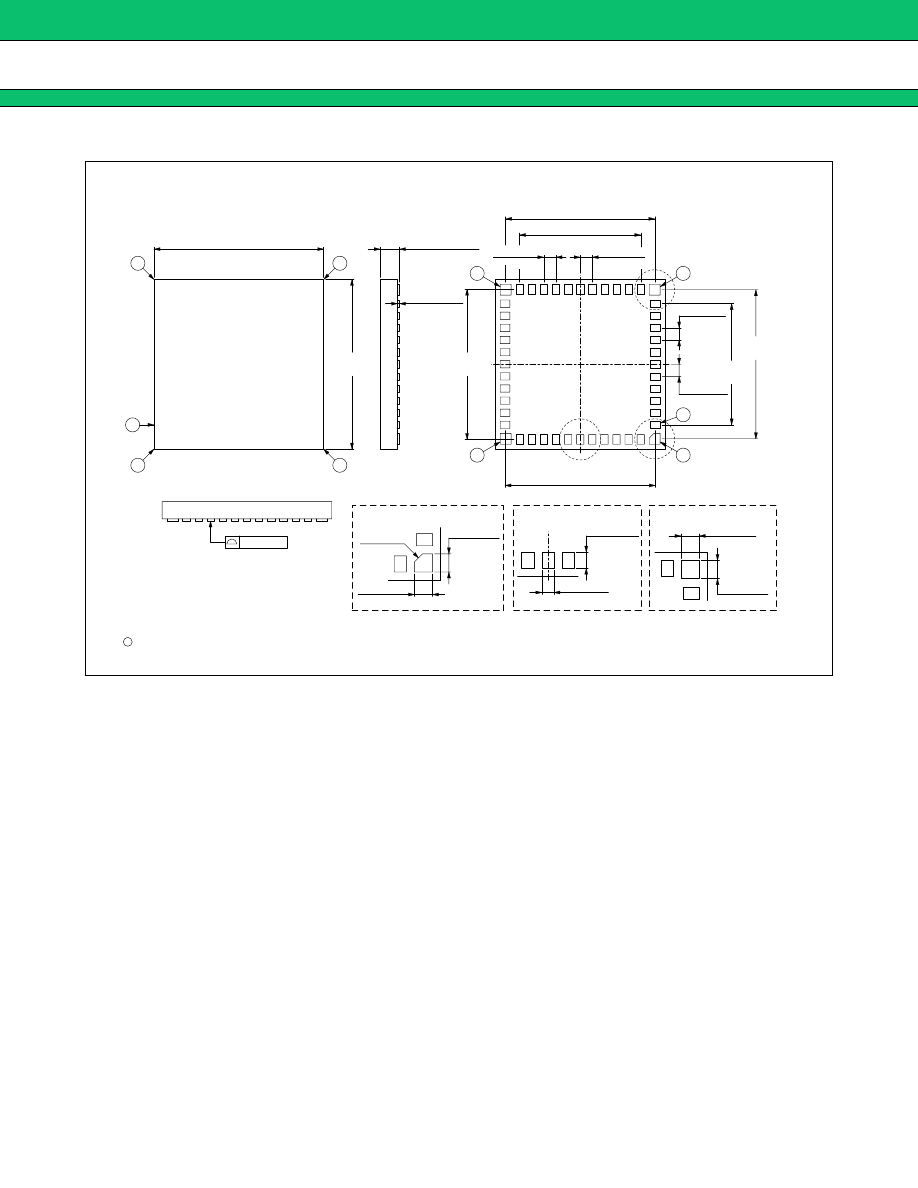
PACKAGE DIMENSIONS
(Continued)
48-pin plastic LQFP
(FPT-48P-M05)
Note : Pins width and pins thickness include plating thickness.
Dimensions in mm (inches)
C
2000 FUJITSU LIMITED F48013S-c-4-8
24
13
36
25
48
37
INDEX
7.00±0.10(.276±.004)SQ
9.00±0.20(.354±.008)SQ
0.145±0.055
(.006±.002)
0.08(.003)
"A"
0°~8°
.059
–.004
+.008
–0.10
+0.20
1.50
0.50±0.20
(.020±.008)
0.60±0.15
(.024±.006)
0.10±0.10
(.004±.004)
(Stand off)
0.25(.010)
Details of "A" part
1
12
0.08(.003)
M
(.008±.002)
0.20±0.05
0.50(.020)
LEAD No.
(Mounting height)
MB3883
38
(Continued)
48-pin plastic BCC
(LCC-48P-M02)
Dimensions in mm (inches)
C
1998 FUJITSU LIMITED C48055SC-1-1
1
13
37
25
0.50±0.10
(.020±.004)
0.50(.020)
TYP
5.00(.197)
TYP
48
6.15(.242)
TYP
"C"
"A"
"B"
6.20(.244)TYP
6.20(.244)
TYP
0.50±0.10
(.020±.004)
0.50(.020)
TYP
5.00(.197)TYP
6.15(.242)TYP
(0.80(.031)MAX)
0.085±0.040
(.003±.002)
13
25
37
1
48
7.00±0.10(.276±.004)
(Stand off)
7.00±0.10
(.276±.004)
0.05(.002)
0.45±0.10
(.018±.004)
0.45±0.10
(.018±.004)
Details of "A" part
C0.2(.008)
0.30±0.10
(.012±.004)
0.40±0.10
(.016±.004)
Details of "B" part
Details of "C" part
0.45±0.10
(.018±.004)
0.45±0.10
(.018±.004)
(Total height)

MB3883
FUJITSU LIMITED
For further information please contact:
Japan
FUJITSU LIMITED
Corporate Global Business Support Division
Electronic Devices
Shinjuku Dai-Ichi Seimei Bldg. 7-1,
Nishishinjuku 2-chome, Shinjuku-ku,
Tokyo 163-0721, Japan
Tel: +81-3-5322-3347
Fax: +81-3-5322-3386
http://edevice.fujitsu.com/
North and South America
FUJITSU MICROELECTRONICS, INC.
3545 North First Street,
San Jose, CA 95134-1804, U.S.A.
Tel: +1-408-922-9000
Fax: +1-408-922-9179
Customer Response Center
Mon. - Fri.: 7 am - 5 pm (PST)
Tel: +1-800-866-8608
Fax: +1-408-922-9179
http://www.fujitsumicro.com/
Europe
FUJITSU MICROELECTRONICS EUROPE GmbH
Am Siebenstein 6-10,
D-63303 Dreieich-Buchschlag,
Germany
Tel: +49-6103-690-0
Fax: +49-6103-690-122
http://www.fujitsu-fme.com/
Asia Pacific
FUJITSU MICROELECTRONICS ASIA PTE. LTD.
#05-08, 151 Lorong Chuan,
New Tech Park,
Singapore 556741
Tel: +65-281-0770
Fax: +65-281-0220
http://www.fmap.com.sg/
Korea
FUJITSU MICROELECTRONICS KOREA LTD.
1702 KOSMO TOWER, 1002 Daechi-Dong,
Kangnam-Gu,Seoul 135-280
Korea
Tel: +82-2-3484-7100
Fax: +82-2-3484-7111
F0101
FUJITSU LIMITED Printed in Japan
All Rights Reserved.
The contents of this document are subject to change without notice.
Customers are advised to consult with FUJITSU sales
representatives before ordering.
The information and circuit diagrams in this document are
presented as examples of semiconductor device applications, and
are not intended to be incorporated in devices for actual use. Also,
FUJITSU is unable to assume responsibility for infringement of
any patent rights or other rights of third parties arising from the use
of this information or circuit diagrams.
The contents of this document may not be reproduced or copied
without the permission of FUJITSU LIMITED.
FUJITSU semiconductor devices are intended for use in standard
applications (computers, office automation and other office
equipments, industrial, communications, and measurement
equipments, personal or household devices, etc.).
CAUTION:
Customers considering the use of our products in special
applications where failure or abnormal operation may directly
affect human lives or cause physical injury or property damage, or
where extremely high levels of reliability are demanded (such as
aerospace systems, atomic energy controls, sea floor repeaters,
vehicle operating controls, medical devices for life support, etc.)
are requested to consult with FUJITSU sales representatives before
such use. The company will not be responsible for damages arising
from such use without prior approval.
Any semiconductor devices have inherently a certain rate of failure.
You must protect against injury, damage or loss from such failures
by incorporating safety design measures into your facility and
equipment such as redundancy, fire protection, and prevention of
over-current levels and other abnormal operating conditions.
If any products described in this document represent goods or
technologies subject to certain restrictions on export under the
Foreign Exchange and Foreign Trade Control Law of Japan, the
prior authorization by Japanese government should be required for
export of those products from Japan.

This datasheet has been download from:
Datasheets for electronics components.
Document Outline
- DESCRIPTION
- FEATURES
- PACKAGES
- PIN ASSIGNMENTS
- PIN DESCRIPTION
- BLOCK DIAGRAM
- ABSOLUTE MAXIMUM RATINGS
- RECOMMENDED OPERATING CONDITIONS
- ELECTRICAL CHARACTERISTICS
- TYPICAL CHARACTERISTICS
- FUNCTIONS
- SETTING THE TRIANGULAR OSCILLATOR FREQUENCY
- SETTING THE OUTPUT VOLTAGE
- SETTING THE OUTPUT CURRENT
- SETTING TIME CONSTANT FOR TIMER-LATCH SHORT-CIRCUIT PROTECTION CIRCUIT
- TREATMENT WITHOUT USING CSCP
- OPERATING WITHOUT THE SOFT START FUNCTION
- SETTING THE DEAD TIME
- TREATMENT WITHOUT USING CH4 INV Amp.
- APPLICATION EXAMPLE
- PARTS LIST
- REFERENCE DATA
- USAGE PRECAUTION
- ORDERING INFORMATION
- PACKAGE DIMENSIONS
Wyszukiwarka
Podobne podstrony:
więcej podobnych podstron