
Tips ‘n Tricks
3V


M
© 2006 Microchip Technology Inc.
DS41285A-page i
Tips ‘N Tricks Introduction
TIP #1:
Powering 3.3V Systems From 5V
Using an LDO Regulator ............................... 4
TIP #2:
Low-Cost Alternative Power System
Using a Zener Diode ..................................... 6
TIP #3:
Lower Cost Alternative Power System
Using 3 Rectifier Diodes ............................... 8
TIP #4:
Powering 3.3V Systems From 5V Using
Switching Regulators .................................. 10
TIP #5:
3.3V – 5V Direct Connect ........................... 13
TIP #6:
3.3V – 5V Using a MOSFET Translator...... 14
TIP #7:
3.3V – 5V Using A Diode Offset..................16
TIP #8:
3.3V – 5V Using A Voltage Comparator ..... 18
TIP #9:
5V – 3.3V Direct Connect ........................... 21
TIP #10: 5V – 3.3V With Diode Clamp ......................22
TIP #11: 5V – 3.3V Active Clamp .............................. 24
TIP #12: 5V – 3.3V Resistor Divider.......................... 25
TIP #13: 3.3V – 5V Level Translators........................ 29
TIP #14: 3.3V – 5V Analog Gain Block......................32
TIP #15: 3.3V – 5V Analog Offset Block....................33
TIP #16: 5V – 3.3V Active Analog Attenuator............ 34
TIP #17: 5V – 3V Analog Limiter ............................... 37
TIP #18: Driving Bipolar Transistors.......................... 41
TIP #19: Driving N-Channel MOSFET Transistors.... 44
Table of Contents
Tips ‘n Tricks

Tips ‘n Tricks
DS41285A-page ii
© 2006 Microchip Technology Inc.
NOTES:

Tips ‘n Tricks
© 2006 Microchip Technology Inc.
DS41285A-page 1
TIPS ‘N TRICKS INTRODUCTION
The 3.3 volt to 5 volt connection.
Overview
One of the by-products of our ever increasing need
for processing speed is the steady reduction in the
size of the transistors used to build
microcontrollers. Up-integration at cheaper cost
also drives the need for smaller geometries. With
reduced size comes a reduction in the transistor
breakdown voltage, and ultimately, a reduction in
the supply voltage when the breakdown voltage
falls below the supply voltage. So, as speeds
increase and complexity mounts, it is an inevitable
consequence that the supply voltages would drop
from 5V to 3.3V, or even 1.8V for high density
devices.
Microchip microcontrollers have reached a
sufficient level of speed and complexity that they
too are making the transition to sub-5V supply
voltages. The challenge is that most of the
interface circuitry is still designed for 5V supplies.
This means that, as designers, we now face the
task of interfacing 3.3V and 5V systems. Further,
the task includes not only logic level translation,
but also powering the 3.3V systems and
translating analog signals across the 3.3V/5V
barrier.

Tips ‘n Tricks
DS41285A-page 2
© 2006 Microchip Technology Inc.
This Tips ‘n Tricks book addresses these
challenges with a collection of power supply
building blocks, digital level translation blocks and
even analog translation blocks. Throughout the
book, multiple options are presented for each of
the transitions, spanning the range from all-in-one
interface devices, to low-cost discrete solutions. In
short, all the blocks a designer is likely to need for
handling the 3.3V challenge, whether the driving
force is complexity, cost or size.
Note:The tips ‘n tricks presented here assume a
3.3V supply. However, the techniques
work equally well for other supply voltages
with the appropriate modifications.
Tips ‘n Tricks
© 2006 Microchip Technology Inc.
DS41285A-page 3
Power Supplies
One of the first 3.3V challenges is generating the
3.3V supply voltage. Given that we are discussing
interfacing 5V systems to 3.3V systems, we can
assume that we have a stable 5 V
DC
supply. This
section will present voltage regulator solutions
designed for the 5V to 3.3V transition. A design
with only modest current requirements may use a
simple linear regulator. Higher current needs may
dictate a switching regulator solution. Cost
sensitive applications may need the simplicity of a
discrete diode regulator. Examples from each of
these areas are included here, with the necessary
support information to adapt to a wide variety of
end applications.
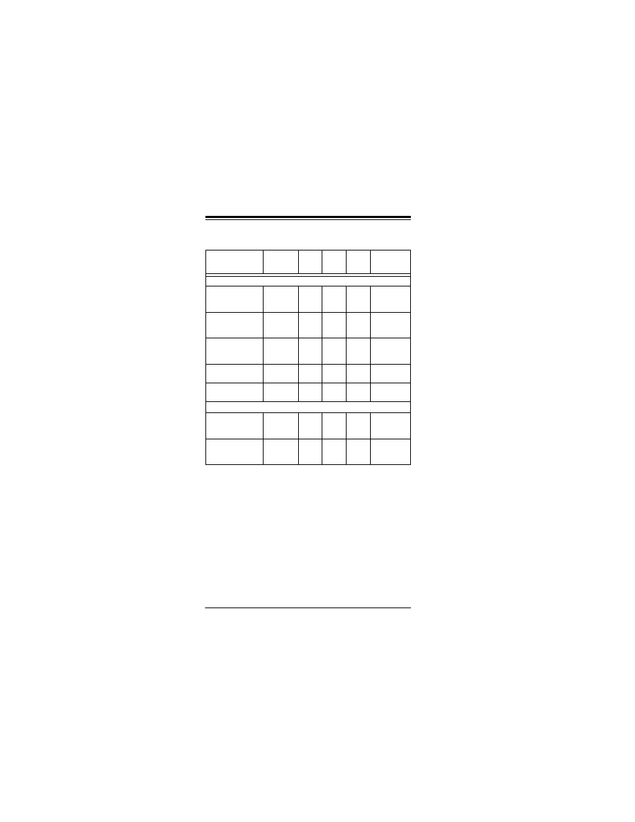
TABLE -1:
POWER SUPPLY COMPARISONS
Method
V
REG
I
Q
Eff.
Size Cost
Transient
Response
Zener
Shun
Reg.
10%
Typ
5 mA
60% Sm
Low
Poor
Series
Linear
Reg.
0.4%
Typ
1
μA
to
100
μA
60% Sm
Med
Excellent
Switching
Buck
Reg.
0.4%
Typ
30
μA
to
2 mA
93% Med
to
Lg
High Good

Tips ‘n Tricks
DS41285A-page 4
© 2006 Microchip Technology Inc.
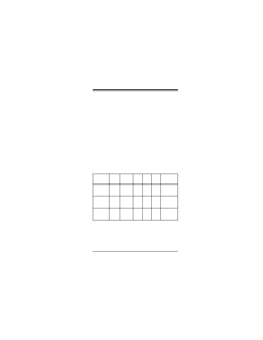
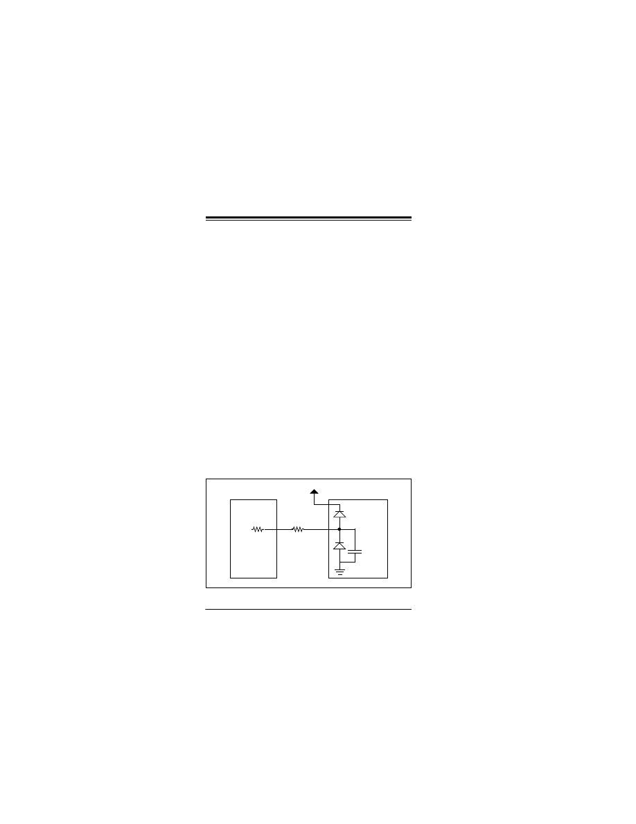
TIP #1
Powering 3.3V Systems From 5V
Using an LDO Regulator
The dropout voltage of standard three-terminal
linear regulators is typically 2.0-3.0V. This
precludes them from being used to convert 5V to
3.3V reliably. Low Dropout (LDO) regulators, with
a dropout voltage in the few hundred milli-volt
range, are perfectly suited for this type of
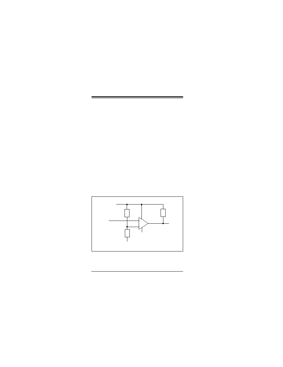
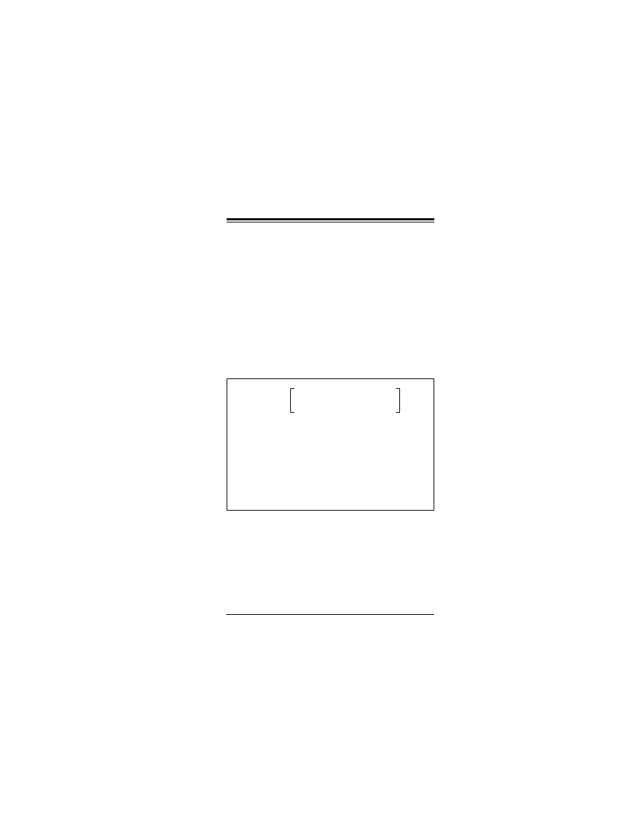
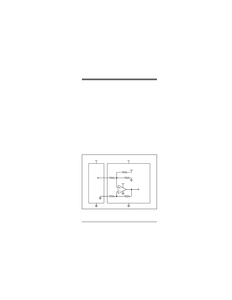
application. Figure 1-1 contains a block diagram of
a basic LDO system with appropriate current
elements labeled. From this figure it can be seen
that an LDO consists of four main elements:
1. pass transistor
2. bandgap reference
3. operational amplifier
4. feedback resistor divider
When selecting an LDO, it is important to know
what distinguishes one LDO from another. Device
quiescent current, package size and type are
important device parameters. Evaluating for each
parameter for the specific application yields an
optimal design.
Tips ‘n Tricks
© 2006 Microchip Technology Inc.
DS41285A-page 5
FIGURE 1-1:
LDO VOLTAGE REGULATOR
An LDOs quiescent current, I
Q
, is the device
ground current, I
GND
, while the device is operating
at no load. I
GND
is the current used by the LDO to
perform the regulating operation. The efficiency of
an LDO can be approximated as the output
voltage divided by the input voltage when
I
OUT
>>I
Q
. However, at light loads, the I
Q
must be
taken into account when calculating the efficiency.
An LDO with lower I
Q
will have a higher light load
efficiency. This increase in light load efficiency has
a negative effect on the LDO performance. Higher
quiescent current LDOs are able to respond
quicker to sudden line and load transitions.
I
IN
V
IN
V
REF
I
OUT
C
1
C
2
I
GND
R
L
Tips ‘n Tricks
DS41285A-page 6
© 2006 Microchip Technology Inc.
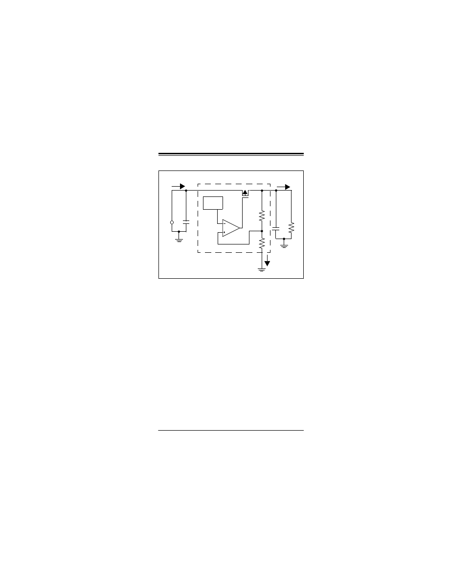
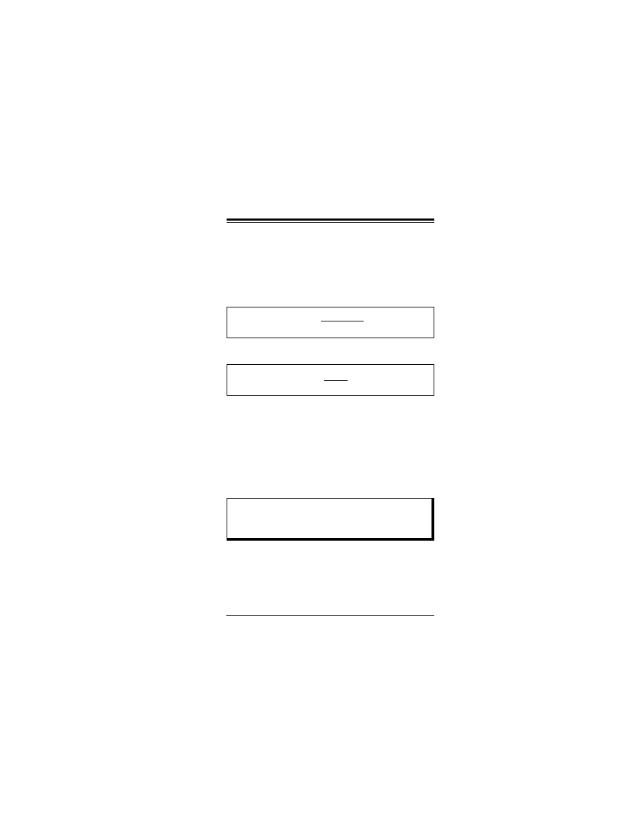
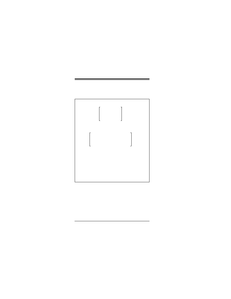
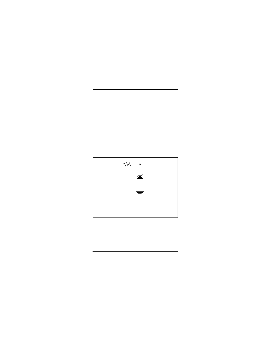
TIP #2
Low-Cost Alternative Power
System Using a Zener Diode
Details a low-cost regulator alternative using a
Zener diode.
FIGURE 2-1:
ZENER SUPPLY
A simple, low-cost 3.3V regulator can be made out
of a Zener diode and a resistor as shown in
Figure 2-1. In many applications, this circuit can be
a cost-effective alternative to using a LDO
regulator. However, this regulator is more load
sensitive than a LDO regulator. Additionally, it is
less energy efficient, as power is always being
dissipated in R
1
and D
1
.
R
1
limits the current to D
1
and the PICmicro
®
MCU
so that V
DD
stays within the allowable range.
Because the reverse voltage across a Zener diode
varies as the current through it changes, the value
of R
1
needs to be considered carefully.
V
DD
V
SS
PICmicro
®
MCU
0.1 uF
C
1
D
1
+5V
R
1
470 Ohm

Tips ‘n Tricks
© 2006 Microchip Technology Inc.
DS41285A-page 7
R
1
must be sized so that at maximum load,
typically when the PICmicro MCU is running and is
driving its outputs high, the voltage drop across R
1
is low enough so that the PICmicro MCU has
enough voltage to operate. Also, R
1
must be sized
so that at minimum load, typically when the
PICmicro MCU is in Reset, that V
DD
does not
exceed either the Zener diode’s power rating or
the maximum V
DD
for the PICmicro MCU.
Tips ‘n Tricks
DS41285A-page 8
© 2006 Microchip Technology Inc.
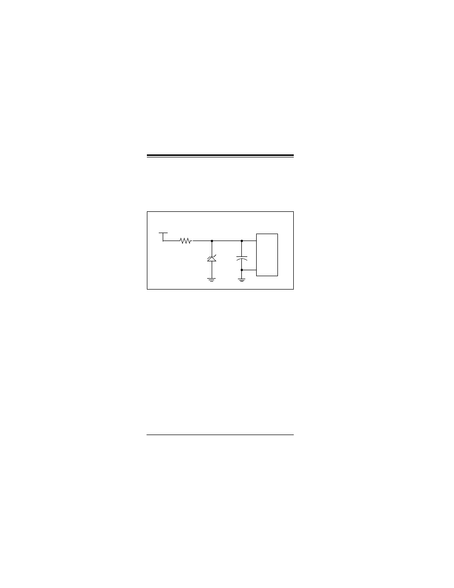
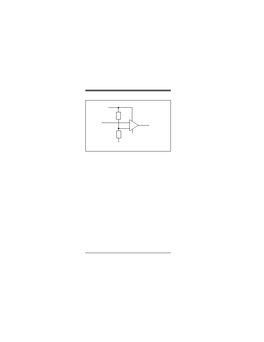
TIP #3
Lower Cost Alternative Power
System Using 3 Rectifier Diodes
Figure 3-1 details a lower cost regulator alternative
using 3 rectifier diodes.
FIGURE 3-1:
DIODE SUPPLY
We can also use the forward drop of a series of
normal switching diodes to drop the voltage going
into the PICmicro MCU. This can be even more
cost-effective than the Zener diode regulator. The
current draw from this design is typically less than
a circuit using a Zener.
V
DD
V
SS
PICmicro
®
MCU
0.1 uF
C
1
R
1
+5V
D
3
D
1
D
2

Tips ‘n Tricks
© 2006 Microchip Technology Inc.
DS41285A-page 9
The number of diodes needed varies based on the
forward voltage of the diode selected. The voltage
drop across diodes D
1
-D
3
is a function of the
current through the diodes. R
1
is present to keep
the voltage at the PICmicro MCUs V
DD
pin from
exceeding the PICmicro MCUs maximum V
DD
at
minimum loads (typically when the PICmicro MCU
is in Reset or sleeping). Depending on the other
circuitry connected to V
DD
, this resistor may have
its value increased or possibly even eliminated
entirely. Diodes D
1
-D
3
must be selected so that at
maximum load, typically when the PICmicro is
running and is driving its outputs high, the voltage
drop across D
1
-D
3
is low enough to meet the
PICmicro MCUs minimum V
DD
requirements.

Tips ‘n Tricks
DS41285A-page 10
© 2006 Microchip Technology Inc.
TIP #4
Powering 3.3V Systems From 5V
Using Switching Regulators
A buck switching regulator, shown in Figure 4-1, is
an inductor-based converter used to step-down an
input voltage source to a lower magnitude output
voltage. The regulation of the output is achieved
by controlling the ON time of MOSFET Q1. Since
the MOSFET is either in a lower or high resistive
state (ON or OFF, respectively), a high source
voltage can be converted to a lower output voltage
very efficiently.
The relationship between the input and output
voltage can be established by balancing the
volt-time of the inductor during both states of Q1.
It therefore follows that for MOSFET Q1:
When choosing an inductor value, a good starting
point is to select a value to produce a maximum
peak-to-peak ripple current in the inductor equal to
ten percent of the maximum load current.
(V
s
– V
o
) *t
on
= V
o
* (T – t
on
)
Where: T
≡ t
on
/Duty_Cycle
Duty_Cycle
Q1
= V
o
/V
s
V = L* (di/dt)
L = (V
s
-V
o
) * (t
on
/I
o
*0.10)
Tips ‘n Tricks
© 2006 Microchip Technology Inc.
DS41285A-page 11
When choosing an output capacitor value, a good
starting point is to set the LC filter characteristic
impedance equal to the load resistance. This
produces an acceptable voltage overshoot when
operating at full load and having the load abruptly
removed.
When choosing a diode for D
1
, choose a device
with a sufficient current rating to handle the
inductor current during the discharge part of the
pulse cycle (I
L
).
FIGURE 4-1:
BUCK REGULATOR
C = L/R
2
= (I
2
* L)/V
2
o
o
Z
o
≡ √ L/C
L
Vo
D
1
C
Q1
Vs
R
L
Tips ‘n Tricks
DS41285A-page 12
© 2006 Microchip Technology Inc.
Digital Interfacing
When interfacing two devices that operate at
different voltages, it is imperative to know the
output and input thresholds of both devices. Once
these values are known, a technique can be
selected for interfacing the devices based on the
other requirements of your application. Table 4-1
contains the output and input thresholds that will
be used throughout this document. When
designing an interface, make sure to reference
your manufacturers data sheet for the actual
threshold levels.
TABLE 4-1:
INPUT/OUTPUT THRESHOLDS
V
OH
min
V
OL
max
V
IH
min
V
IL
max
5V TTL
2.4V
0.5V
2.0V
0.8V
3.3V
LVTTL
2.4V
0.4V
2.0V
0.8V
5V
CMOS
4.7V
(V
CC
-0.3V)
0.5V
3.5V
(0.7xV
CC
)
1.5V
(0.3xV
CC
)
3.3V
LVCMOS
3.0V
(V
CC
-0.3V)
0.5V
2.3V
(0.7xV
CC
)
1.0V
(0.3xV
CC
)

Tips ‘n Tricks
© 2006 Microchip Technology Inc.
DS41285A-page 13
TIP #5
3.3V Æ 5V Direct Connect
The simplest and most desired way to connect a
3.3V output to a 5V input is by a direct connection.
This can be done only if the following 2
requirements are met:
• The V
OH
of the 3.3V output is greater than the
V
IH
of the 5V input
• The V
OL
of the 3.3V output is less than the V
IL
of the 5V input
An example of when this technique can be used is
interfacing a 3.3V LVCMOS output to a 5V TTL
input. From the values given in Table 4-1, it can
clearly be seen that both of these requirements are
met.
3.3V LVCMOS V
OH
of 3.0 volts is greater than 5V
TTL V
IH
of 2.0 volts
and
3.3V LVCMOS V
OL
of 0.5 volts is less than 5V TTL
V
IL
of 0.8 volts.
When both of these requirements are not met,
some additional circuitry will be needed to
interface the two parts. See Tips 6, 7, 8 and 13 for
possible solutions.

Tips ‘n Tricks
DS41285A-page 14
© 2006 Microchip Technology Inc.
TIP #6
3.3V Æ 5V Using a MOSFET
Translator
In order to drive any 5V input that has a higher V
IH
than the V
OH
of a 3.3V CMOS part, some
additional circuitry is needed. A low-cost two
component solution is shown in Figure 6-1.
When selecting the value for R
1,
there are two
parameters that need to be considered; the
switching speed of the input and the current
consumption through R
1
. When switching the
input from a ‘0’ to a ‘1’, you will have to account for
the time the input takes to rise because of the RC
time constant formed by R
1
, and the input
capacitance of the 5V input plus any stray
capacitance on the board. The speed at which you
can switch the input is given by the following:
Since the input and stray capacitance of the board
are fixed, the only way to speed up the switching
of the input is to lower the resistance of R
1
. The
trade-off of lowering the resistance of R
1
to get
faster switching times is the increase in current
draw when the 5V input remains low. The
switching to a ‘0’ will typically be much faster than
switching to a ‘1’ because the ON resistance of the
N-channel MOSFET will be much smaller than R
1
.
Also, when selecting the N-channel FET, select a
FET that has a lower V
GS
threshold voltage than
the V
OH
of 3.3V output.
T
SW
= 3 x R
1
x (C
IN
+ C
S
)
Tips ‘n Tricks
© 2006 Microchip Technology Inc.
DS41285A-page 15
FIGURE 6-1:
MOSFET TRANSLATOR
5V
R
1
5V Input
3.3V
Output
LVCMOS
Tips ‘n Tricks
DS41285A-page 16
© 2006 Microchip Technology Inc.
TIP #7
3.3V Æ 5V Using A Diode Offset
The inputs voltage thresholds for 5V CMOS and
the output drive voltage for 3.3V LVTTL and
LVCMOS are listed in Table 7-1.
TABLE 7-1:
INPUT/OUTPUT THRESHOLDS
Note that both the high and low threshold input
voltages for the 5V CMOS inputs are about a volt
higher than the 3.3V outputs. So, even if the output
from the 3.3V system could be offset, there would
be little or no margin for noise or component
tolerance. What is needed is a circuit that offsets
the outputs and increases the difference between
the high and low output voltages.
FIGURE 7-1:
DIODE OFFSET
5V CMOS
Input
3.3V
LVTTL
Output
3.3V
LVCMOS
Output
High
Threshold
> 3.5V
> 2.4V
> 3.0V
Low
Threshold
< 1.5V
< 0.4V
< 0.5V
5V
R
1
5V Input
3.3V Output
D
1
3.3V
D
2

Tips ‘n Tricks
© 2006 Microchip Technology Inc.
DS41285A-page 17
When output voltage specifications are
determined, it is done assuming that the output is
driving a load between the output and ground for
the high output, and a load between 3.3V and the
output for the low output. If the load for the high
threshold is actually between the output and 3.3V,
then the output voltage is actually much higher as
the load resistor is the mechanism that is pulling
the output up, instead of the output transistor.
If we create a diode offset circuit (see Figure 7-1),
the output low voltage is increased by the forward
voltage of the diode D
1
, typically 0.7V, creating a
low voltage at the 5V CMOS input of 1.1V to 1.2V.
This is well within the low threshold input voltage
for the 5V CMOS input. The output high voltage is
set by the pull-up resistor and diode D
2
, tied to the
3.3V supply. This puts the output high voltage at
approximately 0.7V above the 3.3V supply, or 4.0
to 4.1V, which is well above the 3.5V threshold for
the 5V CMOS input.
Note:For the circuit to work properly, the pull-up
resistor must be significantly smaller than
the input resistance of the 5V CMOS
input, to prevent a reduction in the output
voltage due to a resistor divider effect at
the input. The pull-up resistor must also be
large enough to keep the output current
loading on the 3.3V output within the
specification of the device.
Tips ‘n Tricks
DS41285A-page 18
© 2006 Microchip Technology Inc.
TIP #8
3.3V Æ 5V Using A Voltage
Comparator
The basic operation of the comparator is as
follows:
• When the voltage at the inverting (-) input is
greater than that at the non-inverting (+) input,
the output of the comparator swings to Vss.
• When the voltage at the non-inverting (+) input
is greater than that at the non-inverting (-) input,
the output of the comparator is in a high state.
To preserve the polarity of the 3.3V output, the
3.3V output must be connected to the non-
inverting input of the comparator. The inverting
input of the comparator is connected to a
reference voltage determined by R
1
and R
2
, as
shown in Figure 8-1.
FIGURE 8-1:
COMPARATOR TRANSLATOR
5V (V
DD
)
V
SS
+
–
R
2
R
O
5V Input
R
1
3.3V Output
V
SS
Tips ‘n Tricks
© 2006 Microchip Technology Inc.
DS41285A-page 19
Calculating R
1
and R
2
The ratio of R
1
and R
2
depends on the logic levels
of the input signal. The inverting input should be
set to a voltage halfway between V
OL
and V
OH
for
the 3.3V output. For an LVCMOS output, this
voltage is:
Given that R
1
and R
2
are related by the logic
levels,
assuming a value of 1K for R
2
, R
1
is 1.8K.
An op amp wired up as a comparator can be used
to convert a 3.3V input signal to a 5V output signal.
This is done using the property of the comparator
that forces the output to swing high (V
DD
) or low
(Vss), depending on the magnitude of difference in
voltage between its ‘inverting’ input and ‘non-
inverting’ input.
Note:For the op amp to work properly when
powered by 5V, the output must be
capable of rail-to-rail drive.
1.75V= (3.0V + .5V)
2
R
1
= R
2
5V
1.75V
-1
(
)
Tips ‘n Tricks
DS41285A-page 20
© 2006 Microchip Technology Inc.
FIGURE 8-2:
OP AMP AS A COMPARATOR
5V (V
DD
)
V
SS
+
–
R
2
5V Input
R
1
3.3V Output
V
SS
Tips ‘n Tricks
© 2006 Microchip Technology Inc.
DS41285A-page 21
TIP #9
5V – 3.3V Direct Connect
5V outputs have a typical V
OH
of 4.7 volts and a
V
OL
of 0.4 volts and a 3.3V LVCMOS input will
have a typical V
IH
of 0.7 x V
DD
and a V
IL
of 0.2 x
V
DD
.
When the 5V output is driving low, there are no
problems because the 0.4 volt output is less than
in the input threshold of 0.8 volts. When the 5V
output is high, the V
OH
of 4.7 volts is greater than
2.1 volt V
IH
, therefore, we can directly connect the
2 pins with no conflicts if the 3.3V CMOS input is
5 volt tolerant.
FIGURE 9-1:
5V TOLERANT INPUT
If the 3.3V CMOS input is not 5 volt tolerant, then
there will be an issue because the maximum volt
specification of the input will be exceeded.
See Tips 10-13 for possible solutions.
R
S
5V TTL
Output
3V CMOS
Input
5V Tolerant
with
Tips ‘n Tricks
DS41285A-page 22
© 2006 Microchip Technology Inc.
TIP #10 5V Æ 3.3V With Diode Clamp
Many manufacturers protect their I/O pins from
exceeding the maximum allowable voltage
specification by using clamping diodes. These
clamping diodes keep the pin from going more
than a diode drop below Vss and a diode drop
above V
DD
. To use the clamping diode to protect
the input, you still need to look at the current
through the clamping diode. The current through
the clamp diodes should be kept small (in the
micro amp range). If the current through the
clamping diodes gets too large, then you risk the
part latching up. Since the source resistance of a
5V output is typically around 10 ohms, an
additional series resistor is still needed to limit the
current through the clamping diode as shown
Figure 10-1. The consequence of using the series
resistor is it will reduce the speed at which we can
switch the input because the RC time constant
formed the capacitance of the pin (C
L
).
FIGURE 10-1: CLAMPING DIODES ON THE INPUT
R
S
5V
Output
3.3V
Input
R
SER
C
L
V
DD
Tips ‘n Tricks
© 2006 Microchip Technology Inc.
DS41285A-page 23
If the clamping diodes are not present, a single
external diode can be added to the circuit as
shown in Figure 10-2.
FIGURE 10-2: WITHOUT CLAMPING DIODES
R
S
5V
Output
3.3V
Input
R
SER
C
L
V
DD
D
1
Tips ‘n Tricks
DS41285A-page 24
© 2006 Microchip Technology Inc.
TIP #11 5V Æ 3.3V Active Clamp
One problem with using a diode clamp is that it
injects current onto the 3.3V power supply. In
designs with a high current 5V outputs, and lightly
loaded 3.3V power supply rails, this injected
current can float the 3.3V supply voltage above
3.3V. To prevent this problem, a transistor can be
substituted which routes the excess output drive
current to ground instead of the 3.3V supply.
Figure 11-1 shows the resulting circuit.
FIGURE 11-1: TRANSISTOR CLAMP
The base-emitter junction of Q1 performs the
same function as the diode in a diode clamp
circuit. The difference is that only a small
percentage of the emitter current flows out of the
base of the transistor to the 3.3V rail, the bulk of
the current is routed to the collector where it
passes harmlessly to ground. The ratio of base
current to collector current is dictated by the
current gain of the transistor, typically 10-400,
depending upon which transistor is used.
3.3V
Q1
5V Output
3.3V Input
R
1
Tips ‘n Tricks
© 2006 Microchip Technology Inc.
DS41285A-page 25
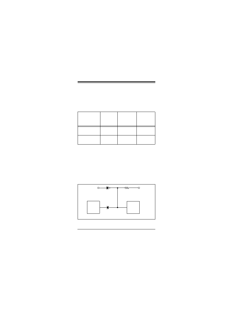
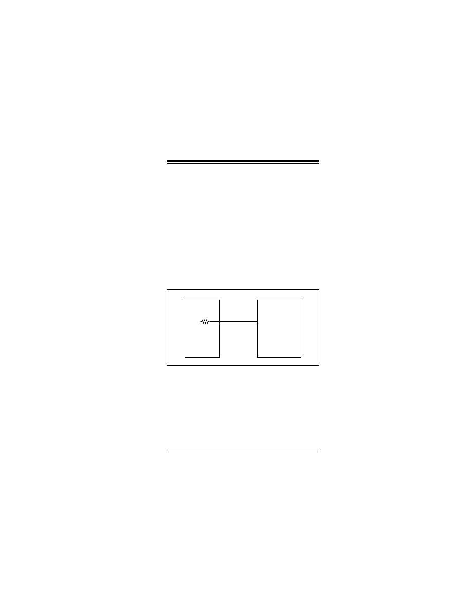
TIP #12 5V Æ 3.3V Resistor Divider
A simple resistor divider can be used to reduce the
output of a 5V device to levels appropriate for a
3.3V device input. An equivalent circuit of this
interface is shown in Figure 12-1.
FIGURE 12-1: RESISTIVE INTERFACE EQUIVALENT
CIRCUIT
Typically, the source resistance, R
S
, is very small
(less than 10 ohms) so its affect on R
1
will be
negligible provided that R
1
is chosen to be much
larger than R
S
. At the receive end, the load resis-
tance, R
L
, is very large (greater than 500 k ohms)
so its affect on R
2
will be negligible provided that
R
2
is chosen to be much less than R
L
.
R
L
C
L
R
1
R
2
R
S
5V Device
3.3V Device
C
S
V
S
V
L

Tips ‘n Tricks
DS41285A-page 26
© 2006 Microchip Technology Inc.
There is a trade-off between power dissipation
and transition times. To keep the power require-
ments of the interface circuit at a minimum, the
series resistance of R
1
and R
2
should be as large
as possible. However, the load capacitance,
which is the combination of the stray capacitance,
C
S
, and the 3.3V device input capacitance, C
L
,
can adversely affect the rise and fall times of the
input signal. Rise and fall times can be unaccept-
ably long if R
1
and R
2
are too large.
Neglecting the affects of R
S
and R
L
, the formula for
determining the values for R
1
and R
2
is given by
EQUATION 12-1:
DIVIDER VALUES
V
S
R1 R2
+
--------------------
V
L
R2
-------
=
R1
V
S
V
L
–
(
) R2
⋅
V
L
-----------------------------------
=
R1
0.515 R2
⋅
=
; Solving for R
1
; Substituting voltages
; General relationship
Tips ‘n Tricks
© 2006 Microchip Technology Inc.
DS41285A-page 27
The formula for determining the rise and fall times
is given in Equation 12-2. For circuit analysis, the
Thevenin equivalent is used to determine the
applied voltage, V
A
, and the series resistance, R.
The Thevenin equivalent is defined as the open
circuit voltage divided by the short circuit current.
The Thevenin equivalent, R, is determined to be
0.66*R
1
and the Thevenin equivalent, V
A
, is
determined to be 0.66*V
S
for the circuit shown in
Figure 12-2 according to the limitations imposed
by Equation 12-2.
EQUATION 12-2:
RISE/FALL TIME
As an example, suppose the following conditions
exist:
• Stray capacitance = 30 pF
• Load capacitance = 5 pF
• Maximum rise time from 0.3V to 3V
≤ 1 μS
• Applied source voltage Vs = 5V
t
R C
V
F
V
A
–
V
I
V
A
–
-------------------
⎝
⎠
⎛
⎞
ln
⋅ ⋅
–
=
Where:
t
= Rise or Fall time
R = 0.66*R
1
C = C
S
+C
L
V
I
= Initial voltage on C (V
L
)
V
F
= Final voltage on C (V
L
)
V
A
= Applied voltage (0.66*V
S
)
Tips ‘n Tricks
DS41285A-page 28
© 2006 Microchip Technology Inc.
The calculation to determine the maximum
resistances is shown in Equation 12-3.
EQUATION 12-3:
EXAMPLE CALCULATION
R
t
C
V
F
V
A
–
V
I
V
A
–
--------------------
⎝
⎠
⎛
⎞
ln
⋅
----------------------------------------
–
=
R
10 10
7
–
⋅
35 10
12
–
3
0.66 5
⋅
(
)
–
0.3
0.66 5
⋅
(
)
–
------------------------------------
⎝
⎠
⎛
⎞
ln
⋅
⋅
------------------------------------------------------------------------------
–
=
R
12408
=
Solve Equation 12-2 for R:
Substitute values:
Thevenin equivalent maximum R:
Solve for maximum R
1
and R
2
:
R1
8190
=
R2
R1
0.515
-------------
=
R1
0.66 R
⋅
=
R2
15902
=

Tips ‘n Tricks
© 2006 Microchip Technology Inc.
DS41285A-page 29
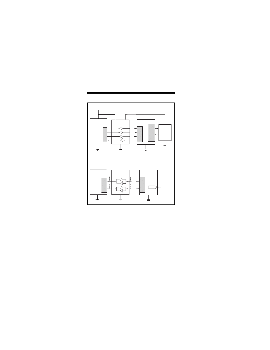
TIP #13 3.3V Æ 5V Level Translators
While level translation can be done discretely, it is
often preferred to use an integrated solution. Level
translators are available in a wide range of
capabilities. There are unidirectional and
bidirectional configurations, different voltage
translations and different speeds, all giving the
user the ability to select the best solution.
Board-level communication between devices
(e.g., MCU to peripheral) is most often done by
either SPI or I
2
C
™
. For SPI, it may be appropriate
to use a unidirectional level translator and for I
2
C,
it is necessary to use a bidirectional solution.
Figure 13-1 below illustrates both solutions.
Tips ‘n Tricks
DS41285A-page 30
© 2006 Microchip Technology Inc.
FIGURE 13-1: LEVEL TRANSLATOR
Low-Power
PICmicro
®
MCU/
dsPIC
®
DSC
Unidirectional
Level Translator
nCS
SCK
SDO
SDI
SPI
MCP2515
MCP2551
CAN
Transceiver
SPI
CAN
V
DD
5.0V
VL
3.3V
Low-Power
PICmicro
®
MCU/
dsPIC
®
DSC
Bidirectional
Level Translator
SCL
SDA
MCP3221
I2C™
V
DD
5.0V
VL
3.3V
12-bit
ADC
I2C™
V
DD
V
DD
VL
VL

Tips ‘n Tricks
© 2006 Microchip Technology Inc.
DS41285A-page 31
Analog
The final 3.3V to 5V interface challenge is the
translation of analog signals across the power
supply barrier. While low level signals will probably
not require external circuitry, signals moving
between 3.3V and 5V systems will be affected by
the change in supply. For example, a 1V peak
analog signal converted by an ADC in a 3.3V
system will have greater resolution than an ADC in
a 5V system, simply because more of the ADCs
range is used to convert the signal in the 3.3V
ADC. Alternately, the relatively higher signal
amplitude in a 3.3V system may have problems
with the system’s lower common mode voltage
limitations.
Therefore, some interface circuitry, to compensate
for the differences, may be needed. This section
will discuss interface circuitry to help alleviate
these problems when the signal makes the
transition between the different supply voltages.
Tips ‘n Tricks
DS41285A-page 32
© 2006 Microchip Technology Inc.
TIP #14 3.3V Æ 5V Analog Gain Block
To scale analog voltage up when going from 3.3V
supply to 5V supply. The 33 k
Ω and 17 kΩ set the
op amp gain so that the full scale range is used in
both sides. The 11 k
Ω resistor limits current back
to the 3.3V circuitry.
FIGURE 14-1: ANALOG GAIN BLOCK
+3.3V
+5.0V
+5.0V
11k
MCP6XXX
17k
33k
+3.3V
+5.0V
+5.0V
11k
MCP6XXX
17k
33k
Tips ‘n Tricks
© 2006 Microchip Technology Inc.
DS41285A-page 33
TIP #15 3.3V Æ 5V Analog Offset Block
Offsetting an analog voltage for translation
between 3.3V and 5V.
Shift an analog voltage from 3.3V supply to 5V
supply. The 147 k
Ω and 30.1 kΩ resistors on the
top right and the +5V supply voltage are equivalent
to a 0.85V voltage source in series with a 25 k
Ω
resistor. This equivalent 25 k
Ω resistance, the
three 25 k
Ω resistors, and the op amp form a
difference amplifier with a gain of 1 V/V. The 0.85V
equivalent voltage source shifts any signal seen at
the input up by the same amount; signals centered
at 3.3V/2 = 1.65V will also be centered at 5.0V/2 =
2.50V. The top left resistor limits current from the
5V circuitry.
FIGURE 15-1: ANALOG OFFSET BLOCK
+3.3V
+5.0V
+5.0V
25k
25k
MCP6XXX
25k
30.1k
147k
+5.0V
+3.3V
+5.0V
+5.0V
25k
25k
MCP6XXX
25k
30.1k
147k
+5.0V
Tips ‘n Tricks
DS41285A-page 34
© 2006 Microchip Technology Inc.
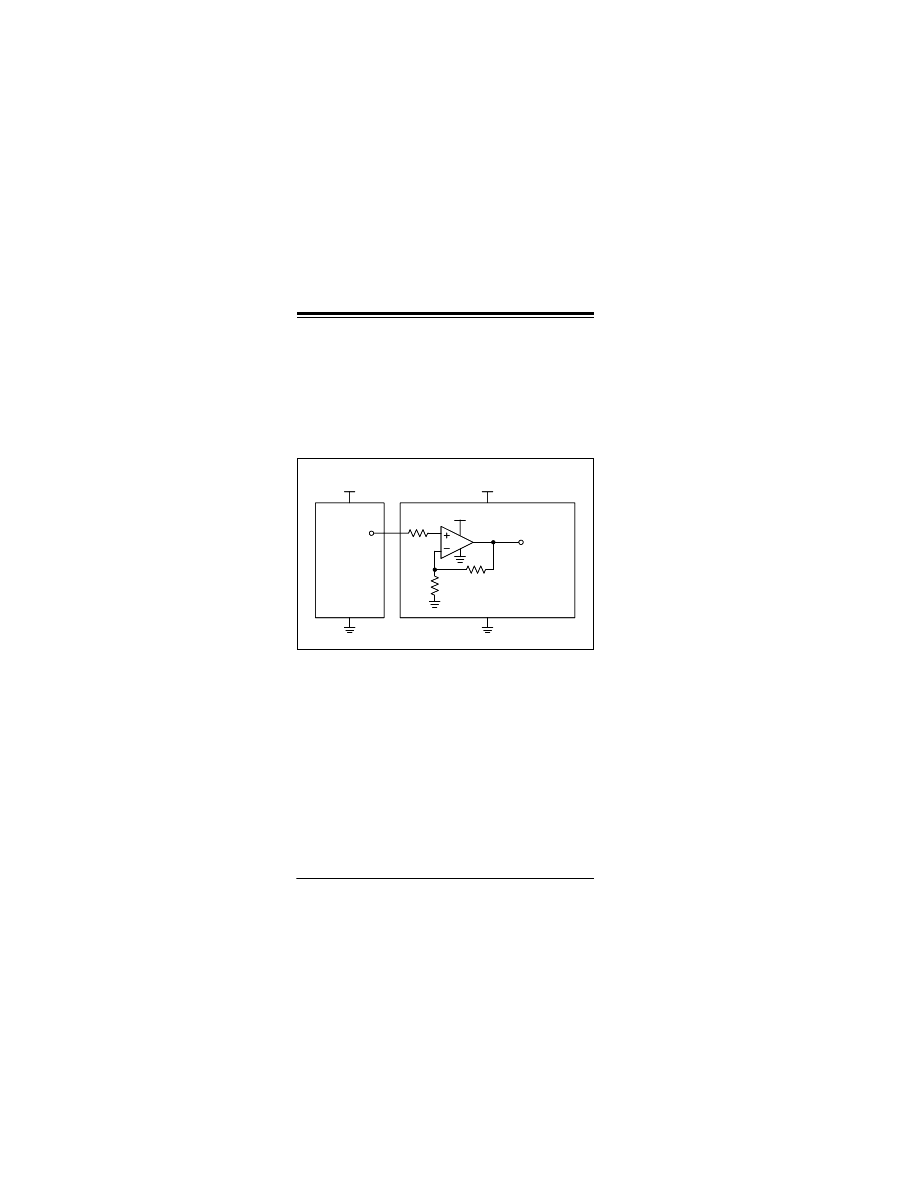
TIP #16 5V Æ 3.3V Active Analog
Attenuator
Reducing a signal’s amplitude from a 5V to 3.3V
system using an op amp.
The simplest method of converting a 5V analog
signal to a 3.3V analog signal is to use a resistor
divider with a ratio R
1
:R
2
of 1.7:3.3. However,
there are a few problems with this.
1) The attenuator may be feeding a capacitive
load, creating an unintentional low pass filter.
2) The attenuator circuit may need to drive a low-
impedance load from a high-impedance source.
Under either of these conditions, an op amp
becomes necessary to buffer the signals.
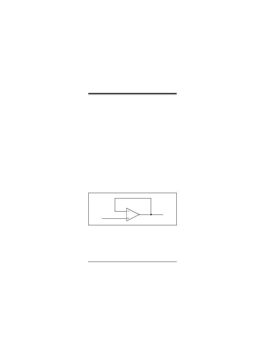
The op amp circuit necessary is a unity gain
follower (see Figure 16-1).
FIGURE 16-1: UNITY GAIN
This circuit will output the same voltage that is
applied to the input.
To convert the 5V signal down to a 3V signal, we
simply add the resistor attenuator.
6
5
7
Tips ‘n Tricks
© 2006 Microchip Technology Inc.
DS41285A-page 35
FIGURE 16-2: OP AMP ATTENUATORS
6
5
7
6
5
7
R
1
R
2
1.7
X
3.3
X
1.7
X
3.3
X
R
2
R
1
(OR)

Tips ‘n Tricks
DS41285A-page 36
© 2006 Microchip Technology Inc.
If the resistor divider is before the unity gain
follower, then the lowest possible impedance is
provided for the 3.3V circuits. Also, the op amp can
be powered from 3.3V, saving some power. If the
X is made very large, then power consumed by the
5V side can be minimized.
If the attenuator is added after the unity gain
follower, then the highest possible impedance is
presented to the 5V source. The op amp must be
powered from 5V and the impedance at the 3V
side will depend upon the value of R
1
||R
2
.

Tips ‘n Tricks
© 2006 Microchip Technology Inc.
DS41285A-page 37
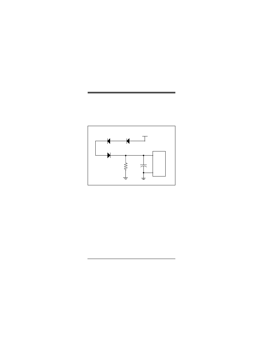
TIP #17 5V Æ 3V Analog Limiter
When moving a 5V signal down to a 3.3V system,
it is sometimes possible to use the attenuation as
gain. If the desired signal is less than 5V, then
attaching that signal to a 3.3V ADC will result in
larger conversion values. The danger is when the
signal runs to the 5V rail. A method is therefore
required to control the out-of-range voltages while
leaving the in-range voltages unaffected. Three
ways to accomplish this will be discussed here.
1. Using a diode to clamp the overvoltage to
the 3.3V supply.
2. Using a Zener diode to clamp the voltage to
any desired limit.
3. Using an op amp with a diode to perform a
precision clamp.
Tips ‘n Tricks
DS41285A-page 38
© 2006 Microchip Technology Inc.
The simplest method to perform the overvoltage
clamp is identical to the simple method of
interfacing a 5V digital signal to the 3.3V digital
signals. A resistor and a diode are used to direct
excess current into the 3.3V supply. The resistor
must be sized to protect the diode and the 3.3V
supply while not adversely affecting the analog
performance. If the impedance of the 3.3V supply
is too low, then this type of clamp can cause the
3.3V supply voltage to increase. Even if the 3.3V
supply has a good low-impedance, this type of
clamp will allow the input signal to add noise to the
3.3V supply when the diode is conducting and if
the frequency is high enough, even when the
diode is not conducting due to the parasitic
capacitance across the diode.
FIGURE 17-1: DIODE CLAMP
+3.3V
D
1
V
OUT
V
IN
R
1
V
OUT
= 3.3V + V
F
if V
IN
> 3.3V + V
F
V
OUT
= V
IN
if V
IN
≤ 3.3V + V
F
V
F
is the forward drop of the diode.
Tips ‘n Tricks
© 2006 Microchip Technology Inc.
DS41285A-page 39
To prevent the input signal from affecting the
supply or to make the input more robust to larger
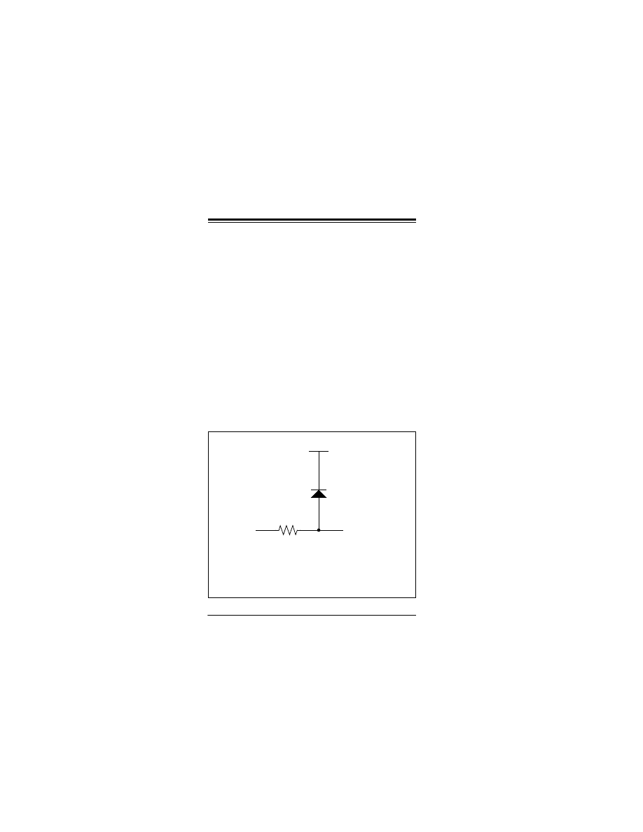
transients, a variation is to use a Zener diode. The
Zener diode is slower than the fast signal diode
typically used in the first circuit. However, they are
generally more robust and do not rely on the
characteristics of the power supply to perform the
clamping. The amount of clamping they provide is
dependant upon the current through the diode.
This is set by the value of R
1
. R
1
may not be
required if the output impedance of the V
IN
source
is sufficiently large.
FIGURE 17-2: ZENER CLAMP
V
OUT
V
IN
R
1
D
1
V
OUT
= V
BR
if V
IN
> V
BR
V
OUT
= V
IN
if V
IN
≤ V
BR
V
BR
is the reverse breakdown voltage of
the Zener diode.
Tips ‘n Tricks
DS41285A-page 40
© 2006 Microchip Technology Inc.
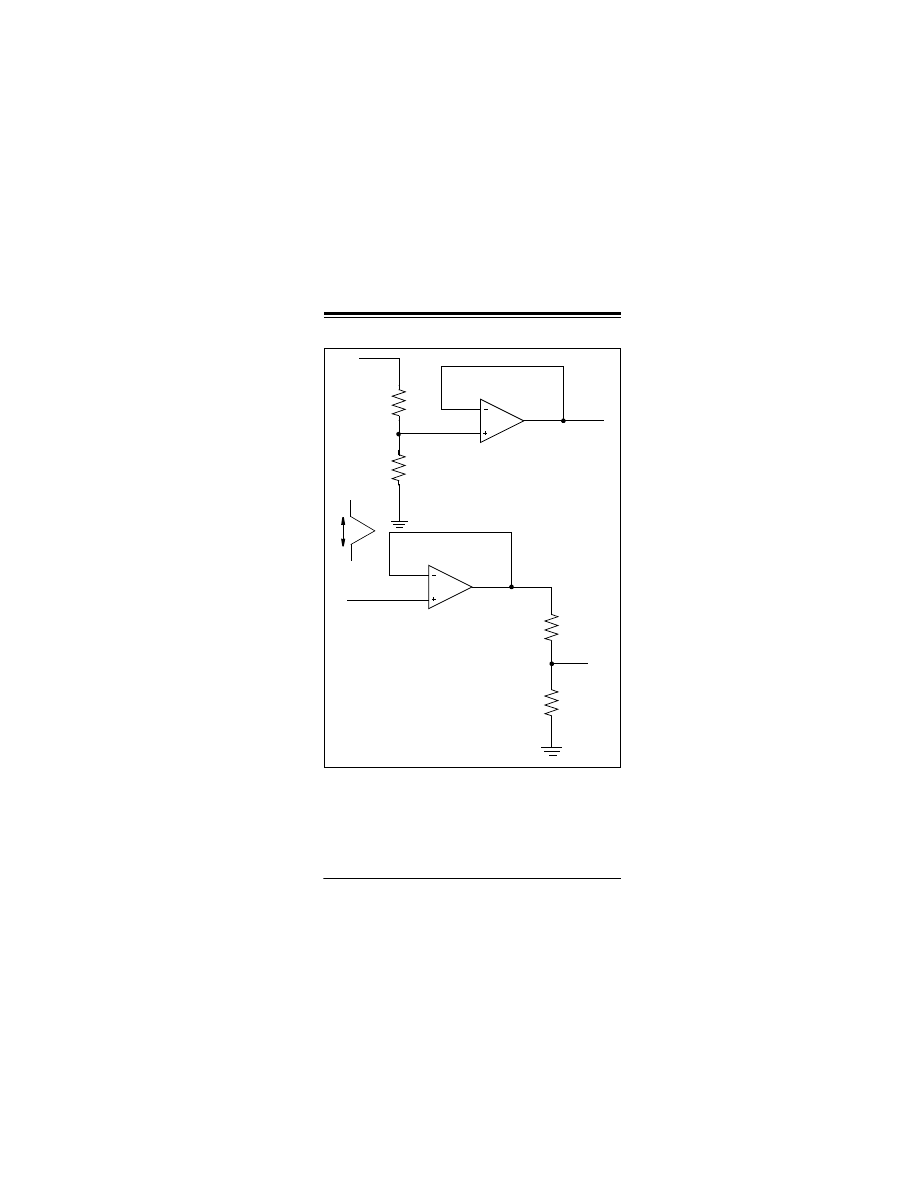
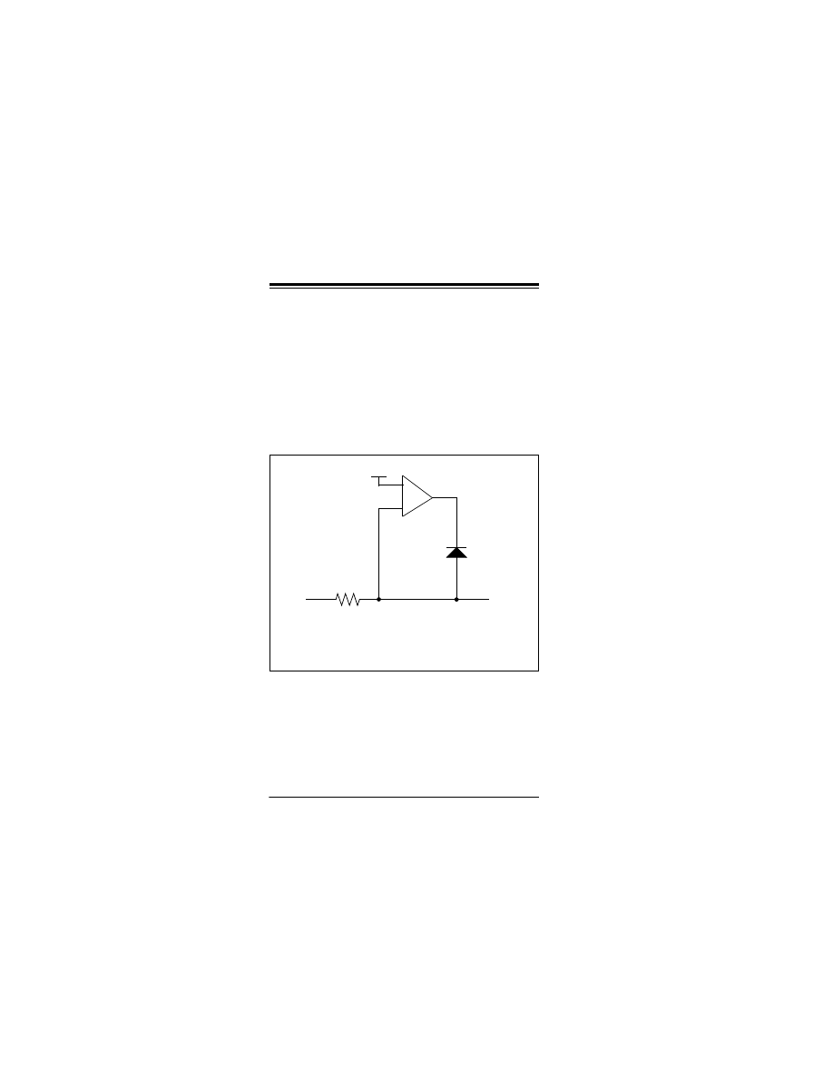
If a more precise overvoltage clamp is required
that does not rely upon the supply, then an op amp
can be employed to create a precision diode. In
Figure 17-3, such a circuit is shown. The op amp
compensates for the forward drop in the diode and
causes the voltage to be clamped at exactly the
voltage supplied on the non-inverting input to the
op amp. The op amp can be powered from 3.3V if
it is rail-to-rail.
FIGURE 17-3: PRECISION DIODE CLAMP
Because the clamping is performed by the op amp,
there is no affect on the power supply. The
impedance presented to the low voltage circuit is
not improved by the op amp, it remains R
1
in
addition to the source circuit impedance.
+3.3V
D
1
V
OUT
V
IN
R
1
+
-
5
6
V
OUT
= 3.3V if V
IN
> 3.3V
V
OUT
= V
IN
if V
IN
≤ 3.3V
Tips ‘n Tricks
© 2006 Microchip Technology Inc.
DS41285A-page 41
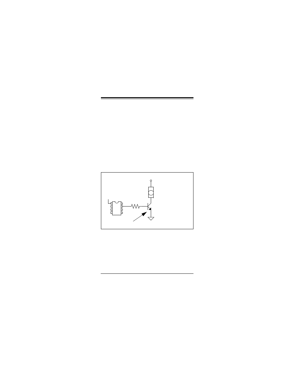
TIP #18 Driving Bipolar Transistors
When driving Bipolar transistors, the amount of
base current “drive” and forward current gain
(
Β/h
FE
) will determine how much current the
transistor can sink. When driven by a
microcontroller I/O port, the base drive current is
calculated using the port voltage and the port
current limit (typically 20 mA). When using 3.3V
technology, smaller value base current limiting
resistors should be used to ensure sufficient base
drive to saturate the transistor.
FIGURE 18-1: DRIVING BIPOLAR TRANSISTORS USING
MICROCONTROLLER I/O PORT
The value of R
BASE
will depend on the
microcontroller supply voltage. Equation 18-1
describes how to calculate R
BASE
.
V
BE
Forward Drop
+
-
R
LOAD
V
LOAD
h
FE
(Forward Gain)
+V
DD
R
BASE
Tips ‘n Tricks
DS41285A-page 42
© 2006 Microchip Technology Inc.
TABLE 18-1:
BIPOLAR TRANSISTOR DC
SPECIFICATIONS
When using bipolar transistors as switches to turn
on and off loads controlled by the microcontroller
I/O port pin, use the minimum h
FE
specification
and margin to ensure complete device saturation.
Characteristic
Sym
Min
Max
Unit
Test
Condition
OFF CHARACTERISTICS
Collector-Base
Breakdown
voltage
V(
BR
)
CBO
60
—
V
I
C
= 50
μA,
I
E
= 0
Collector-
Emitter Break-
down Voltage
V(
BR
)
CEO
50
—
V
I
C
= 1.0 mA,
I
B
= 0
Emitter-Base
Breakdown
Voltage
V(
BR
)
EBO
7.0
—
V
I
E
= 50
μA,
I
C
= 0
Collector Cutoff
Current
I
CBO
—
100
nA
V
CB
= 60V
Emitter Cutoff
Current
I
EBO
—
100
nA
V
EB
= 7.0V
ON CHARACTERISTICS
DC Current Gain
h
FE
120
180
270
270
390
560
—
V
CE
= 6.0V,
I
C
= 1.0 mA
Collector-
Emitter Saturation
Voltage
V
CE
(
SAT
)
—
0.4
V
I
C
= 50 mA,
I
B
= 5.0 mA

Tips ‘n Tricks
© 2006 Microchip Technology Inc.
DS41285A-page 43
EQUATION 18-1:
CALCULATING THE BASE RESISTOR
VALUE
3V technology example:
V
DD
= +3V, V
LOAD
= +40V, R
LOAD
= 400
Ω, h
FE
min. = 180, V
BE
= 0.7V
R
BASE
= 4.14 k
Ω, I/O port current = 556 μA
5V technology example:
V
DD
= +5V, V
LOAD
= +40V, R
LOAD
= 400
Ω, h
FE
min. = 180, V
BE
= 0.7V
R
BASE
= 7.74 k
Ω, I/O port current = 556 μA
For both examples, it is good practice to increase
base current for margin. Driving the base with 1 mA
to 2 mA would ensure saturation at the expense of
increasing the input power consumption.
R
BASE
=
(V
DD
– V
BE
)
X
h
FE
X
R
LOAD
V
LOAD
Tips ‘n Tricks
DS41285A-page 44
© 2006 Microchip Technology Inc.
TIP #19 Driving N-Channel MOSFET
Transistors
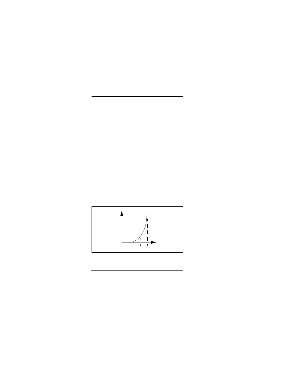
Care must be taken when selecting an external
N-Channel MOSFET for use with a 3.3V
microcontroller. The MOSFET gate threshold
voltage is an indication of the device’s capability
to completely saturate. For 3.3V applications,
select MOSFETs that have an ON resistance
rating for gate drive of 3V or less. For example, a
FET that is rated for 250 uA of drain current with
1V applied from gate-to-source is not necessarily
going to deliver satisfactory results for 100 mA
load with a 3.3V drive. When switching from 5V to
3V technology, review the gate-to-source
threshold and ON resistance characteristics very
carefully as shown in Figure 19-1. A small
decrease in gate drive voltage can significantly
reduce drain current.
FIGURE 19-1: DRAIN CURRENT CAPABILITY VERSUS
GATE TO SOURCE VOLTAGE
I
D
V
T
V
GS
0
0
3.3V 5V
Tips ‘n Tricks
© 2006 Microchip Technology Inc.
DS41285A-page 45
Low threshold devices commonly exist for
MOSFETs with drain-to-source voltages rated
below 30V. MOSFETs with drain-to-source
voltages above 30V typically have higher gate
thresholds (VT).
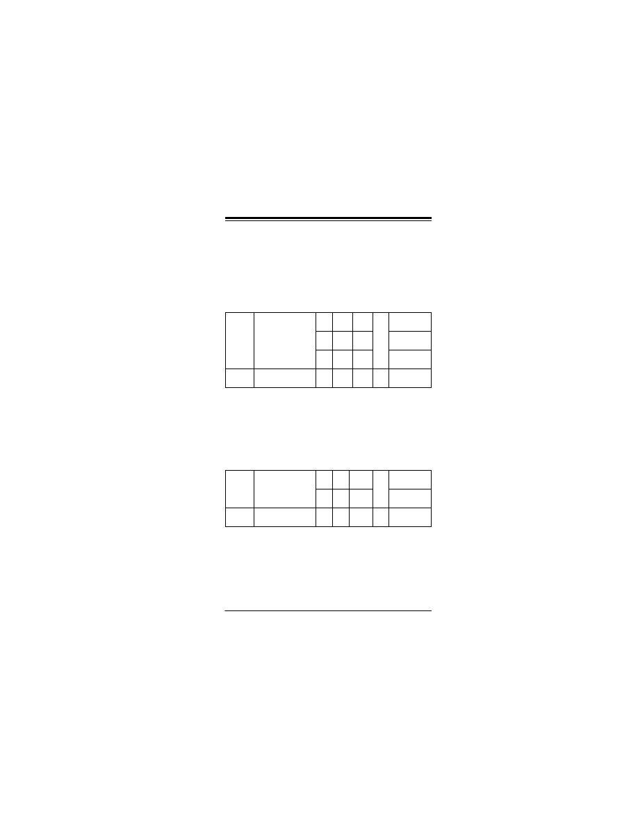
TABLE 19-1:
RDS(ON) AND VGS(TH) SPECIFICATIONS
FOR IRF7467
As shown in Table 19-1, the threshold voltage for
this 30V, N-Channel MOSFET switch is 0.6V. The
resistance rating for this MOSFET is 35 m
Ω with
2.8V applied gate, as a result, this device is well
suited for 3.3V applications.
TABLE 19-2:
RDS(ON) AND VGS(TH) SPECIFICATIONS
FOR IRF7201
R
DS
(on)
Static Drain-to-
Source
On-Resistance
—
9.4
12
m
Ω
V
GS
= 10V,
I
D
= 11A
—
10.6
13.5
V
GS
= 4.5V,
I
D
= 9.0A
—
17
35
V
GS
= 2.8V,
I
D
= 5.5A
V
GS
(th)
Gate Threshold
Voltage
0.6
—
2.0
V
V
DS
= V
GS
,
I
D
= 250
μA
R
DS
(on)
Static Drain-to-
Source
On-Resistance
—
—
0.030
Ω
V
GS
= 10V,
I
D
= 7.3A
—
—
0.050
V
GS
= 4.5V,
I
D
= 3.7A
V
GS
(th)
Gate Threshold
Voltage
1.0
—
—
V
V
DS
= V
GS
,
I
D
= 250
μA

Tips ‘n Tricks
DS41285A-page 46
© 2006 Microchip Technology Inc.
For the IRF7201 data sheet specifications, the
gate threshold voltage is specified as a 1.0V
minimum. This does not mean the device can be
used to switch current with a 1.0V gate-to-source
voltage as there is no RDS(ON) specification for
V
GS
(th) values below 4.5V. This device is not
recommended for 3.3V drive applications that
require low switch resistance but can be used for
5V drive applications.

© 2006 Microchip Technology Inc.
DS41285A-page 47
Additional Online Resources can be found:
www.microchip.com/3volts
• Application Notes
• Migration Documents
• 3 Volt Newsletter
• FAQ’s

Tips ‘n Tricks
DS41285A-page 48
© 2006 Microchip Technology Inc.
NOTES:

© 2006 Microchip Technology Inc.
DS41285A-page 49
Information contained in this publication regarding device applica-
tions and the like is provided only for your convenience and may be
superseded by updates. It is your responsibility to ensure that your
application meets with your specifications. MICROCHIP MAKES
NO REPRESENTATIONS OR WARRANTIES OF ANY KIND
WHETHER EXPRESS OR IMPLIED, WRITTEN OR ORAL, STAT-
UTORY OR OTHERWISE, RELATED TO THE INFORMATION,
INCLUDING BUT NOT LIMITED TO ITS CONDITION, QUALITY,
PERFORMANCE, MERCHANTABILITY OR FITNESS FOR PUR-
POSE. Microchip disclaims all liability arising from this information
and its use. Use of Microchip’s products as critical components in
life support systems is not authorized except with express written
approval by Microchip. No licenses are conveyed, implicitly or
otherwise, under any Microchip intellectual property rights.
Trademarks
The Microchip name and logo, the Microchip logo, Accuron,
dsPIC, K
EE
L
OQ
, microID, MPLAB, PIC, PICmicro, PICSTART,
PRO MATE, PowerSmart, rfPIC, and SmartShunt are registered
trademarks of Microchip Technology Incorporated in the U.S.A.
and other countries.
AmpLab, FilterLab, Migratable Memory, MXDEV, MXLAB,
SEEVAL, SmartSensor and The Embedded Control Solutions
Company are registered trademarks of Microchip Technology
Incorporated in the U.S.A.
Analog-for-the-Digital Age, Application Maestro, dsPICDEM,
dsPICDEM.net, dsPICworks, ECAN, ECONOMONITOR,
FanSense, FlexROM, fuzzyLAB, In-Circuit Serial Programming,
ICSP, ICEPIC, Linear Active Thermistor, MPASM, MPLIB,
MPLINK, MPSIM, PICkit, PICDEM, PICDEM.net, PICLAB,
PICtail, PowerCal, PowerInfo, PowerMate, PowerTool, REAL
ICE, rfLAB, rfPICDEM, Select Mode, Smart Serial, SmartTel,
Total Endurance, UNI/O, WiperLock and Zena are trademarks of
Microchip Technology Incorporated in the U.S.A. and other
countries.
SQTP is a service mark of Microchip Technology Incorporated in
the U.S.A.
All other trademarks mentioned herein are property of their
respective companies.
© 2006, Microchip Technology Incorporated, Printed in the
U.S.A., All Rights Reserved.
Printed on recycled paper.
M
DS41285A-page 50
© 2006 Microchip Technology Inc.
Worldwide Sales and Service
AMERICAS
Corporate Office
Tel: 480-792-7200
Technical Support:
http://support.micro-
chip.com
Atlanta
Tel: 770-640-0034
Boston
Tel: 774-760-0087
Chicago
Tel: 630-285-0071
Dallas
Tel: 972-818-7423
Detroit
Tel: 248-538-2250
Kokomo
Tel: 765-864-8360
Los Angeles
Tel: 949-462-9523
San Jose
Tel: 650-215-1444
Toronto
Tel: 905-673-0699
ASIA/PACIFIC
Australia
Tel: 61-2-9868-6733
China-Beijing
Tel: 86-10-8528-2100
China-Chengdu
Tel: 86-28-8676-6200
China-Fuzhou
Tel: 86-591-8750-
3506
China-Hong Kong
SAR
Tel: 852-2401-1200
China-Qingdao
Tel: 86-532-8502-
7355
China-Shanghai
Tel: 86-21-5407-5533
China-Shenyang
Tel: 86-24-2334-2829
China-Shenzhen
Tel: 86-755-8203-
2660
China-Shunde
Tel: 86-757-2839-
5507
China-Wuhan
Tel: 86-27-5980-5300
China-Xian
Tel: 86-29-8833-7250
India-Bangalore
Tel: 91-80-4182-8400
India-New Delhi
Tel: 91-11-5160-8631
India-Pune
Tel: 91-20-2566-1512
Japan
Tel: 81-45-471- 6166
Korea-Gumi
Tel: 82-54-473-4301
Korea-Seoul
Tel: 82-2-554-7200
Malaysia
Tel: 60-4-646-8870
Philippines
Tel: 63-2-634-9065
Singapore
Tel: 65-6334-8870
Taiwan-Hsin Chu
Tel: 886-3-572-9526
Taiwan-Kaohsiung
Tel: 886-7-536-4818
Taiwan-Taipei
Tel: 886-2-2500-6610
Thailand
Tel: 66-2-694-1351
EUROPE
Austria
Tel: 43-7242-2244-399
Denmark
Tel: 45-4450-2828
France
Tel: 33-1-69-53-63-20
Germany
Tel: 49-89-627-144-0
Italy
Tel: 39-0331-742611
Netherlands
Tel: 31-416-690399
Spain
Tel: 34-91-708-08-90
England
Tel: 44-118-921-5869
02/16/06
Microchip received ISO/TS-16949:2002 quality system
certification for its worldwide headquarters, design and
wafer fabrication facilities in Chandler and Tempe,
Arizona and Mountain View, California in October 2003.
The Company’s quality system processes and procedures
are for its PICmicro
®
8-bit MCUs, K
EE
L
OQ®
code hopping
devices, Serial EEPROMs, microperipherals, nonvolatile
memory and analog products. In addition, Microchip’s
quality system for the design and manufacture of
development systems is ISO 9001:2000 certified.


Microchip Technology Inc.
2355 W. Chandler Blvd. • Chandler, AZ 85224 U.S.A.
Phone: 480-792-7200 • Fax: 480-792-9210
www.microchip.com
© 2006, Microchip Technology Inc., 3/06 DS41285A
*DS41285A*
Document Outline
- Tips ‘N Tricks Introduction
- TIP #1 Powering 3.3V Systems From 5V Using an LDO Regulator
- TIP #2 Low-Cost Alternative Power System Using a Zener Diode
- TIP #3 Lower Cost Alternative Power System Using 3 Rectifier Diodes
- TIP #4 Powering 3.3V Systems From 5V Using Switching Regulators
- TIP #5 3.3V ‡ 5V Direct Connect
- TIP #6 3.3V ‡ 5V Using a MOSFET Translator
- TIP #7 3.3V ‡ 5V Using A Diode Offset
- TIP #8 3.3V ‡ 5V Using A Voltage Comparator
- TIP #9 5V – 3.3V Direct Connect
- TIP #10 5V ‡ 3.3V With Diode Clamp
- TIP #11 5V ‡ 3.3V Active Clamp
- TIP #12 5V ‡ 3.3V Resistor Divider
- TIP #13 3.3V ‡ 5V Level Translators
- TIP #14 3.3V ‡ 5V Analog Gain Block
- TIP #15 3.3V ‡ 5V Analog Offset Block
- TIP #16 5V ‡ 3.3V Active Analog Attenuator
- TIP #17 5V ‡ 3V Analog Limiter
- TIP #18 Driving Bipolar Transistors
- TIP #19 Driving N-Channel MOSFET Transistors
- Trademarks
- Worldwide Sales
Wyszukiwarka
Podobne podstrony:
Windows XP tips&tricks
el tips tricks2
Autodesk Inventor Tutorials Tips & Tricks
Woodworking Tips & Tricks
The Sims [PC] Tips & Tricks
The Sims 2 [PC] Tips & Tricks
Kitchen Hacks The Ultimate Collection Of Secrets, Tips, & Tricks
microsoft microsoft outlook and exchange server tips and tricks FWWF6QVBJHAJ3XOZIQG3OOK3PXKVZKIW3KW
MATLAB array manipulation tips and tricks (ang)
5800 Tips and Tricks
Tips and Tricks for Atari 400 800
Fringe Tips and Ideas
interview tips
Miernik mocy wyjściowej, Różne porady z elektroniki elektrotechniki( tricks)
(ebook) CIA Book of Dirty Tricks1id 1301
Part10 The Role JIP Plays, 4 Important Tips
więcej podobnych podstron