L78S00
SERIES
January 1993
2A POSITIVE VOLTAGE REGULATORS
.
OUTPUT CURRENT TO 2A
.
OUTPUT VOLTAGES OF 5 ; 7.5 ; 9 ; 10 ; 12 ; 15 ;
18 ; 24V
.
THERMAL OVERLOAD PROTECTION
.
SHORT CIRCUIT PROTECTION
.
OUTPUT TRANSISTOR SOA PROTECTION
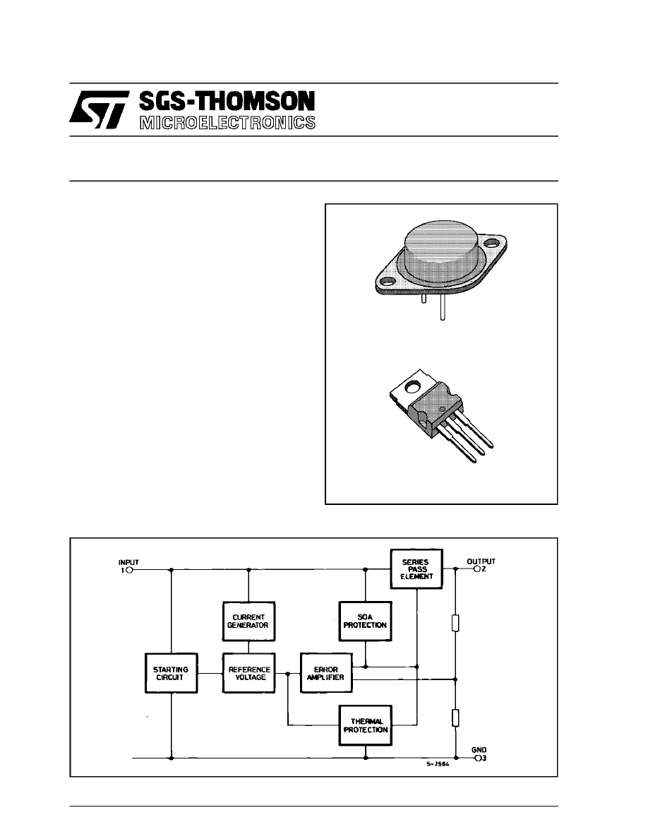
DESCRIPTION
The L78S00 series of three-terminal positive regu-
lators is available in TO-220 and TO-3 packages
and with several fixed output voltages, making it
useful in a wide range of applications. These regu-
lators can provide local on-card regulation, eliminat-
ing the distribution problems associated with single
point regulation. Each type employs internal current
limiting, thermal shut-down and safe area protec-
tion, making it essentially indestructible. If adequate
heat sinking is provided, they can deliver over 2A
output current. Although designed primarily as fixed
voltage regulators, these devices can be used with
external components to obtain adjustable voltages
and currents.
TO-220
BLOCK DIAGRAM
TO-3
1/21
ABSOLUTE MAXIMUM RATINGS
Symbol
Parameter
Val ue
Unit
V
i
DC Input Voltage (for V
o
= 5 to 18V)
(for V
o
= 24V)
35
40
V
V
I
o
Output Current
Internally limited
P
t o t
Power Dissipation
Internally limited
T
s t g
Storage Temperature
– 65 to + 150
°
C
T
o p
Operating Junction Temperature (for L78S00 )
(for L78S00C )
– 55 to + 150
0 to + 150
°
C
°
C
THERMAL DATA
TO-220
TO-3
R
t h j- cas e
R
t h j -amb
Thermal Resistance Junction-case
Thermal Resistance Junction-ambient
Max
Max
3
50
4
35
°
C/W
°
C/W
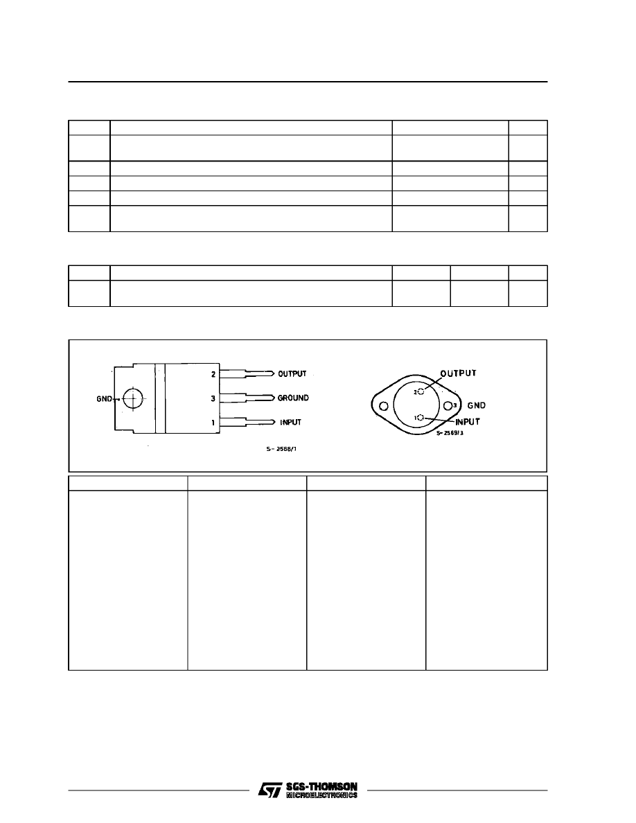
CONNECTION DIAGRAMS AND ORDERING NUMBERS (top views)
Type
T O- 22 0
T O - 3
Output Voltage
L78S05
L78S05C
L78S75
L78S75C
L78S09
L78S09C
L78S10
L78S10C
L78S12
L78S12C
L78S15
L78S15C
L78S18
L78S18C
L78S24
L78S24C
L78S05CV
L78S75CV
L78S09CV
L78S10CV
L78S12CV
L78S15CV
L78S18CV
L78S24CV
L78S05T
L78S05CT
L78S75T
L78S75CT
L78S09T
L78S09CT
L78S10T
L78S10CT
L78S12T
L78S12CT
L78S15T
L78S15CT
L78S18T
L78S18CT
L78S24T
L78S24CT
5 V
5 V
7.5V
7.5V
9 V
9 V
10V
10V
12V
12V
15V
15V
18V
18V
24V
24V
L78S00 SERIES
2/21
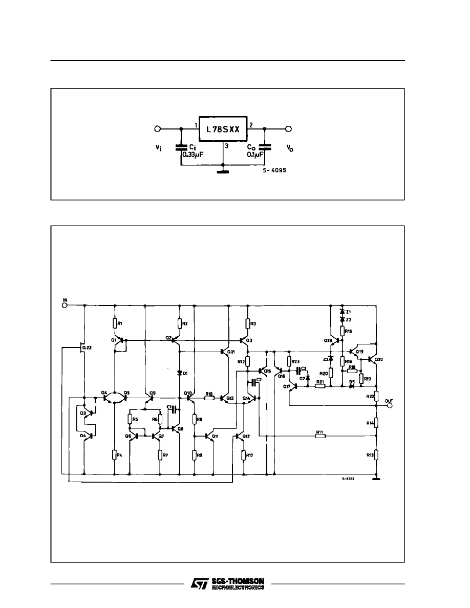
APPLICATION CIRCUIT
SCHEMATIC DIAGRAM
L78S00 SERIES
3/21
TEST CIRCUITS
Figure 1 : DC Parameters.
Figure 2 : Load Regulation.
Figure 3 : Ripple Rejection.
L78S00 SERIES
4/21

ELECTRICAL CHARACTERISTICS FOR L78S05 (refer to the test circuits, T
j
= 25
o
C,
V
i
= 10V, I
o
= 500 mA unless otherwise specified)
Symbol
Parameter
Test Conditions
Min.
Typ.
Max.
Unit
V
o
Output Voltage
4.8
5
5.2
V
V
o
Output Voltage
I
o
= 1 A
V
i
= 7 V
4.75
5
5.25
V
∆
V
o
Line Regulation
V
i
= 7 to 25 V
V
i
= 8 to 25 V
100
50
mV
mV
∆
V
o
Load Regulation
I
o
= 20 mA to 2 A
100
mV
I
d
Quiescent Current
8
mA
∆
I
d
Quiescent Current Change
I
o
= 20 mA to 1A
0.5
mA
∆
I
d
Quiescent Current Change
I
o
= 20 mA
V
i
= 7 to 25 V
1.3
mA
∆
V
o
∆
T
Output Voltage Drift
I
o
= 5 mA
T
j
= -55 to 150
o
C
-1.1
mV/
o
C
e
N
Output Noise Voltage
B = 10Hz to 100KHz
40
µ
V
SVR
Supply Voltage Rejection
f = 120 Hz
60
dB
V
i
Operating Input Voltage
I
o
≤
1.5 A
8
V
R
o
Output Resistance
f = 1KHz
17
m
Ω
I
sc
Short Circuit Current
V
i
= 27 V
500
mA
I
scp
Short Circuit Peack Current
3
A
ELECTRICAL CHARACTERISTICS FOR L78S75 (refer to the test circuits, T
j
= 25
o
C,
V
i
= 12.5V, I
o
= 500 mA unless otherwise specified)
Symbol
Parameter
Test Conditions
Min.
Typ.
Max.
Unit
V
o
Output Voltage
7.15
7.5
7.9
V
V
o
Output Voltage
I
o
= 1 A
V
i
= 9.5 V
7.1
7.5
7.95
V
∆
V
o
Line Regulation
V
i
= 9.5 to 25 V
V
i
= 10.5 to 20 V
120
60
mV
mV
∆
V
o
Load Regulation
I
o
= 20 mA to 2 A
120
mV
I
d
Quiescent Current
8
mA
∆
I
d
Quiescent Current Change
I
o
= 20 mA to 1A
0.5
mA
∆
I
d
Quiescent Current Change
I
o
= 20 mA
V
i
= 9.5 to 25 V
1.3
mA
∆
V
o
∆
T
Output Voltage Drift
I
o
= 5 mA
T
j
= -55 to 150
o
C
-0.8
mV/
o
C
e
N
Output Noise Voltage
B = 10Hz to 100KHz
52
µ
V
SVR
Supply Voltage Rejection
f = 120 Hz
54
dB
V
i
Operating Input Voltage
I
o
≤
1.5 A
10.5
V
R
o
Output Resistance
f = 1KHz
16
m
Ω
I
sc
Short Circuit Current
V
i
= 27 V
500
mA
I
scp
Short Circuit Peack Current
3
A
L78S00 SERIES
5/21
ELECTRICAL CHARACTERISTICS FOR L78S09 (refer to the test circuits, T
j
= 25
o
C,
V
i
= 14V, I
o
= 500 mA unless otherwise specified)
Symbol
Parameter
Test Conditions
Min.
Typ.
Max.
Unit
V
o
Output Voltage
8.65
9
9.35
V
V
o
Output Voltage
I
o
= 1 A
V
i
= 11 V
8.6
9
9.4
V
∆
V
o
Line Regulation
V
i
= 11 to 25 V
V
i
= 11 to 20 V
130
65
mV
mV
∆
V
o
Load Regulation
I
o
= 20 mA to 2 A
130
mV
I
d
Quiescent Current
8
mA
∆
I
d
Quiescent Current Change
I
o
= 20 mA to 1A
0.5
mA
∆
I
d
Quiescent Current Change
I
o
= 20 mA
V
i
= 11 to 25 V
1.3
mA
∆
V
o
∆
T
Output Voltage Drift
I
o
= 5 mA
T
j
= -55 to 150
o
C
-1
mV/
o
C
e
N
Output Noise Voltage
B = 10Hz to 100KHz
60
µ
V
SVR
Supply Voltage Rejection
f = 120 Hz
53
dB
V
i
Operating Input Voltage
I
o
≤
1.5 A
12
V
R
o
Output Resistance
f = 1KHz
17
m
Ω
I
sc
Short Circuit Current
V
i
= 27 V
500
mA
I
scp
Short Circuit Peack Current
3
A
ELECTRICAL CHARACTERISTICS FOR L78S10 (refer to the test circuits, T
j
= 25
o
C,
V
i
= 15V, I
o
= 500 mA unless otherwise specified)
Symbol
Parameter
Test Conditions
Min.
Typ.
Max.
Unit
V
o
Output Voltage
9.5
10
10.5
V
V
o
Output Voltage
I
o
= 1 A
V
i
= 12.5 V
9.4
10
10.6
V
∆
V
o
Line Regulation
V
i
= 12.5 to 30 V
V
i
= 14 to 22 V
200
100
mV
mV
∆
V
o
Load Regulation
I
o
= 20 mA to 2 A
150
mV
I
d
Quiescent Current
8
mA
∆
I
d
Quiescent Current Change
I
o
= 20 mA to 1A
0.5
mA
∆
I
d
Quiescent Current Change
I
o
= 20 mA
V
i
= 12.5 to 30 V
1
mA
∆
V
o
∆
T
Output Voltage Drift
I
o
= 5 mA
T
j
= -55 to 150
o
C
-1
mV/
o
C
e
N
Output Noise Voltage
B = 10Hz to 100KHz
65
µ
V
SVR
Supply Voltage Rejection
f = 120 Hz
53
dB
V
i
Operating Input Voltage
I
o
≤
1.5 A
13
V
R
o
Output Resistance
f = 1KHz
17
m
Ω
I
sc
Short Circuit Current
V
i
= 27 V
500
mA
I
scp
Short Circuit Peack Current
3
A
L78S00 SERIES
6/21

ELECTRICAL CHARACTERISTICS FOR L78S12 (refer to the test circuits, T
j
= 25
o
C,
V
i
= 19V, I
o
= 500 mA unless otherwise specified)
Symbol
Parameter
Test Conditions
Min.
Typ.
Max.
Unit
V
o
Output Voltage
11.5
12
12.5
V
V
o
Output Voltage
I
o
= 1 A
V
i
= 14.5 V
11.4
12
12.6
V
∆
V
o
Line Regulation
V
i
= 14.5 to 30 V
V
i
= 16 to 22 V
240
120
mV
mV
∆
V
o
Load Regulation
I
o
= 20 mA to 2 A
160
mV
I
d
Quiescent Current
8
mA
∆
I
d
Quiescent Current Change
I
o
= 20 mA to 1A
0.5
mA
∆
I
d
Quiescent Current Change
I
o
= 20 mA
V
i
= 14.5 to 30 V
1
mA
∆
V
o
∆
T
Output Voltage Drift
I
o
= 5 mA
T
j
= -55 to 150
o
C
-1
mV/
o
C
e
N
Output Noise Voltage
B = 10Hz to 100KHz
75
µ
V
SVR
Supply Voltage Rejection
f = 120 Hz
53
dB
V
i
Operating Input Voltage
I
o
≤
1.5 A
15
V
R
o
Output Resistance
f = 1KHz
18
m
Ω
I
sc
Short Circuit Current
V
i
= 27 V
500
mA
I
scp
Short Circuit Peack Current
3
A
ELECTRICAL CHARACTERISTICS FOR L78S15 (refer to the test circuits, T
j
= 25
o
C,
V
i
= 23V, I
o
= 500 mA unless otherwise specified)
Symbol
Parameter
Test Conditions
Min.
Typ.
Max.
Unit
V
o
Output Voltage
14.4
15
15.6
V
V
o
Output Voltage
I
o
= 1 A
V
i
= 17.5 V
14.25
15
15.75
V
∆
V
o
Line Regulation
V
i
= 17.5 to 30 V
V
i
= 20 to 26 V
300
150
mV
mV
∆
V
o
Load Regulation
I
o
= 20 mA to 2 A
180
mV
I
d
Quiescent Current
8
mA
∆
I
d
Quiescent Current Change
I
o
= 20 mA to 1A
0.5
mA
∆
I
d
Quiescent Current Change
I
o
= 20 mA
V
i
= 17.5 to 30 V
1
mA
∆
V
o
∆
T
Output Voltage Drift
I
o
= 5 mA
T
j
= -55 to 150
o
C
-1
mV/
o
C
e
N
Output Noise Voltage
B = 10Hz to 100KHz
90
µ
V
SVR
Supply Voltage Rejection
f = 120 Hz
52
dB
V
i
Operating Input Voltage
I
o
≤
1.5 A
18
V
R
o
Output Resistance
f = 1KHz
19
m
Ω
I
sc
Short Circuit Current
V
i
= 27 V
500
mA
I
scp
Short Circuit Peack Current
3
A
L78S00 SERIES
7/21

ELECTRICAL CHARACTERISTICS FOR L78S18 (refer to the test circuits, T
j
= 25
o
C,
V
i
= 26V, I
o
= 500 mA unless otherwise specified)
Symbol
Parameter
Test Conditions
Min.
Typ.
Max.
Unit
V
o
Output Voltage
17.1
18
18.9
V
V
o
Output Voltage
I
o
= 1 A
V
i
= 20.5 V
17
18
19
V
∆
V
o
Line Regulation
V
i
= 20.5 to 30 V
V
i
= 22 to 28 V
360
180
mV
mV
∆
V
o
Load Regulation
I
o
= 20 mA to 2 A
200
mV
I
d
Quiescent Current
8
mA
∆
I
d
Quiescent Current Change
I
o
= 20 mA to 1A
0.5
mA
∆
I
d
Quiescent Current Change
I
o
= 20 mA
V
i
= 22 to 33 V
1
mA
∆
V
o
∆
T
Output Voltage Drift
I
o
= 5 mA
T
j
= -55 to 150
o
C
-1
mV/
o
C
e
N
Output Noise Voltage
B = 10Hz to 100KHz
110
µ
V
SVR
Supply Voltage Rejection
f = 120 Hz
49
dB
V
i
Operating Input Voltage
I
o
≤
1.5 A
21
V
R
o
Output Resistance
f = 1KHz
22
m
Ω
I
sc
Short Circuit Current
V
i
= 27 V
500
mA
I
scp
Short Circuit Peack Current
3
A
ELECTRICAL CHARACTERISTICS FOR L78S24 (refer to the test circuits, T
j
= 25
o
C,
V
i
= 33V, I
o
= 500 mA unless otherwise specified)
Symbol
Parameter
Test Conditions
Min.
Typ.
Max.
Unit
V
o
Output Voltage
23
24
25
V
V
o
Output Voltage
I
o
= 1 A
V
i
= 27 V
22.8
24
25.2
V
∆
V
o
Line Regulation
V
i
= 27 to 38 V
V
i
= 30 to 36 V
480
240
mV
mV
∆
V
o
Load Regulation
I
o
= 20 mA to 2 A
250
mV
I
d
Quiescent Current
8
mA
∆
I
d
Quiescent Current Change
I
o
= 20 mA to 1A
0.5
mA
∆
I
d
Quiescent Current Change
I
o
= 20 mA
V
i
= 8 to 25 V
1
mA
∆
V
o
∆
T
Output Voltage Drift
I
o
= 5 mA
T
j
= -55 to 150
o
C
-1.5
mV/
o
C
e
N
Output Noise Voltage
B = 10Hz to 100KHz
170
µ
V
SVR
Supply Voltage Rejection
f = 120 Hz
48
dB
V
i
Operating Input Voltage
I
o
≤
1.5 A
27
V
R
o
Output Resistance
f = 1KHz
23
m
Ω
I
sc
Short Circuit Current
V
i
= 27 V
500
mA
I
scp
Short Circuit Peack Current
3
A
L78S00 SERIES
8/21

ELECTRICAL CHARACTERISTICS FOR L78S05C (refer to the test circuits, T
j
= 25
o
C,
V
i
= 10V, I
o
= 500 mA unless otherwise specified)
Symbol
Parameter
Test Conditions
Min.
Typ.
Max.
Unit
V
o
Output Voltage
4.8
5
5.2
V
V
o
Output Voltage
I
o
= 1 A
V
i
= 7 V
4.75
5
5.25
V
∆
V
o
Line Regulation
V
i
= 7 to 25 V
V
i
= 8 to 12 V
100
50
mV
mV
∆
V
o
Load Regulation
I
o
= 20 mA to 1.5 A
I
o
= 2 A
80
100
mV
I
d
Quiescent Current
8
mA
∆
I
d
Quiescent Current Change
I
o
= 20 mA to 1A
0.5
mA
∆
I
d
Quiescent Current Change
I
o
= 20 mA
V
i
= 7 to 25 V
1.3
mA
∆
V
o
∆
T
Output Voltage Drift
I
o
= 5 mA
T
j
= 0 to 70
o
C
-1.1
mV/
o
C
e
N
Output Noise Voltage
B = 10Hz to 100KHz
40
µ
V
SVR
Supply Voltage Rejection
f = 120 Hz
54
dB
V
i
Operating Input Voltage
I
o
≤
1.5 A
8
V
R
o
Output Resistance
f = 1KHz
17
m
Ω
I
sc
Short Circuit Current
V
i
= 27 V
500
mA
I
scp
Short Circuit Peack Current
3
A
ELECTRICAL CHARACTERISTICS FOR L78S75C (refer to the test circuits, T
j
= 25
o
C,
V
i
= 12.5V, I
o
= 500 mA unless otherwise specified)
Symbol
Parameter
Test Conditions
Min.
Typ.
Max.
Unit
V
o
Output Voltage
7.15
7.5
7.9
V
V
o
Output Voltage
I
o
= 1 A
V
i
= 9.5 V
7.1
7.5
7.95
V
∆
V
o
Line Regulation
V
i
= 9.5 to 25 V
V
i
= 10.5 to 20 V
120
60
mV
mV
∆
V
o
Load Regulation
I
o
= 20 mA to 1.5 A
I
o
= 2 A
100
140
mV
I
d
Quiescent Current
8
mA
∆
I
d
Quiescent Current Change
I
o
= 20 mA to 1A
0.5
mA
∆
I
d
Quiescent Current Change
I
o
= 20 mA
V
i
= 9.5 to 25 V
1.3
mA
∆
V
o
∆
T
Output Voltage Drift
I
o
= 5 mA
T
j
= 0 to 70
o
C
-0.8
mV/
o
C
e
N
Output Noise Voltage
B = 10Hz to 100KHz
52
µ
V
SVR
Supply Voltage Rejection
f = 120 Hz
48
dB
V
i
Operating Input Voltage
I
o
≤
1.5 A
10.5
V
R
o
Output Resistance
f = 1KHz
16
m
Ω
I
sc
Short Circuit Current
V
i
= 27 V
500
mA
I
scp
Short Circuit Peack Current
3
A
L78S00 SERIES
9/21

ELECTRICAL CHARACTERISTICS FOR L78S09C (refer to the test circuits, T
j
= 25
o
C,
V
i
= 14V, I
o
= 500 mA unless otherwise specified)
Symbol
Parameter
Test Conditions
Min.
Typ.
Max.
Unit
V
o
Output Voltage
8.65
9
9.35
V
V
o
Output Voltage
I
o
= 1 A
V
i
= 11 V
8.6
9
9.4
V
∆
V
o
Line Regulation
V
i
= 11 to 25 V
V
i
= 11 to 20 V
130
65
mV
mV
∆
V
o
Load Regulation
I
o
= 20 mA to 1.5 A
I
o
= 2 A
100
170
mV
I
d
Quiescent Current
8
mA
∆
I
d
Quiescent Current Change
I
o
= 20 mA to 1A
0.5
mA
∆
I
d
Quiescent Current Change
I
o
= 20 mA
V
i
= 11 to 25 V
1.3
mA
∆
V
o
∆
T
Output Voltage Drift
I
o
= 5 mA
T
j
= 0 to 70
o
C
-1
mV/
o
C
e
N
Output Noise Voltage
B = 10Hz to 100KHz
60
µ
V
SVR
Supply Voltage Rejection
f = 120 Hz
47
dB
V
i
Operating Input Voltage
I
o
≤
1.5 A
12
V
R
o
Output Resistance
f = 1KHz
17
m
Ω
I
sc
Short Circuit Current
V
i
= 27 V
500
mA
I
scp
Short Circuit Peack Current
3
A
ELECTRICAL CHARACTERISTICS FOR L78S10C (refer to the test circuits, T
j
= 25
o
C,
V
i
= 15V, I
o
= 500 mA unless otherwise specified)
Symbol
Parameter
Test Conditions
Min.
Typ.
Max.
Unit
V
o
Output Voltage
9.5
10
10.5
V
V
o
Output Voltage
I
o
= 1 A
V
i
= 12.5 V
9.4
10
10.6
V
∆
V
o
Line Regulation
V
i
= 12.5 to 30 V
V
i
= 14 to 22 V
200
100
mV
mV
∆
V
o
Load Regulation
I
o
= 20 mA to 1.5 A
I
o
= 2 A
150
240
mV
I
d
Quiescent Current
8
mA
∆
I
d
Quiescent Current Change
I
o
= 20 mA to 1A
0.5
mA
∆
I
d
Quiescent Current Change
I
o
= 20 mA
V
i
= 12.5 to 30 V
1
mA
∆
V
o
∆
T
Output Voltage Drift
I
o
= 5 mA
T
j
= 0 to 70
o
C
-1
mV/
o
C
e
N
Output Noise Voltage
B = 10Hz to 100KHz
65
µ
V
SVR
Supply Voltage Rejection
f = 120 Hz
47
dB
V
i
Operating Input Voltage
I
o
≤
1.5 A
13
V
R
o
Output Resistance
f = 1KHz
17
m
Ω
I
sc
Short Circuit Current
V
i
= 27 V
500
mA
I
scp
Short Circuit Peack Current
3
A
L78S00 SERIES
10/21

ELECTRICAL CHARACTERISTICS FOR L78S12C (refer to the test circuits, T
j
= 25
o
C,
V
i
= 19V, I
o
= 500 mA unless otherwise specified)
Symbol
Parameter
Test Conditions
Min.
Typ.
Max.
Unit
V
o
Output Voltage
11.5
12
12.5
V
V
o
Output Voltage
I
o
= 1 A
V
i
= 14.5 V
11.4
12
12.6
V
∆
V
o
Line Regulation
V
i
= 14.5 to 30 V
V
i
= 16 to 22 V
240
120
mV
mV
∆
V
o
Load Regulation
I
o
= 20 mA to 1.5 A
I
o
= 2 A
150
240
mV
I
d
Quiescent Current
8
mA
∆
I
d
Quiescent Current Change
I
o
= 20 mA to 1A
0.5
mA
∆
I
d
Quiescent Current Change
I
o
= 20 mA
V
i
= 14.5 to 30 V
1
mA
∆
V
o
∆
T
Output Voltage Drift
I
o
= 5 mA
T
j
= 0 to 70
o
C
-1
mV/
o
C
e
N
Output Noise Voltage
B = 10Hz to 100KHz
75
µ
V
SVR
Supply Voltage Rejection
f = 120 Hz
47
dB
V
i
Operating Input Voltage
I
o
≤
1.5 A
15
V
R
o
Output Resistance
f = 1KHz
18
m
Ω
I
sc
Short Circuit Current
V
i
= 27 V
500
mA
I
scp
Short Circuit Peack Current
3
A
ELECTRICAL CHARACTERISTICS FOR L78S15C (refer to the test circuits, T
j
= 25
o
C,
V
i
= 23V, I
o
= 500 mA unless otherwise specified)
Symbol
Parameter
Test Conditions
Min.
Typ.
Max.
Unit
V
o
Output Voltage
14.4
15
15.6
V
V
o
Output Voltage
I
o
= 1 A
V
i
= 17.5 V
14.25
15
15.75
V
∆
V
o
Line Regulation
V
i
= 17.5 to 30 V
V
i
= 20 to 26 V
300
150
mV
mV
∆
V
o
Load Regulation
I
o
= 20 mA to 1.5 A
I
o
= 2 A
150
300
mV
I
d
Quiescent Current
8
mA
∆
I
d
Quiescent Current Change
I
o
= 20 mA to 1A
0.5
mA
∆
I
d
Quiescent Current Change
I
o
= 20 mA
V
i
= 17.5 to 30 V
1
mA
∆
V
o
∆
T
Output Voltage Drift
I
o
= 5 mA
T
j
= 0 to 70
o
C
-1
mV/
o
C
e
N
Output Noise Voltage
B = 10Hz to 100KHz
90
µ
V
SVR
Supply Voltage Rejection
f = 120 Hz
46
dB
V
i
Operating Input Voltage
I
o
≤
1.5 A
18
V
R
o
Output Resistance
f = 1KHz
19
m
Ω
I
sc
Short Circuit Current
V
i
= 27 V
500
mA
I
scp
Short Circuit Peack Current
3
A
L78S00 SERIES
11/21
ELECTRICAL CHARACTERISTICS FOR L78S18C (refer to the test circuits, T
j
= 25
o
C,
V
i
= 26V, I
o
= 500 mA unless otherwise specified)
Symbol
Parameter
Test Conditions
Min.
Typ.
Max.
Unit
V
o
Output Voltage
17.1
18
18.9
V
V
o
Output Voltage
I
o
= 1 A
V
i
= 20.5 V
17
18
19
V
∆
V
o
Line Regulation
V
i
= 20.5 to 30 V
V
i
= 22 to 28 V
360
180
mV
mV
∆
V
o
Load Regulation
I
o
= 20 mA to 1.5 A
I
o
= 2 A
200
360
mV
I
d
Quiescent Current
8
mA
∆
I
d
Quiescent Current Change
I
o
= 20 mA to 1A
0.5
mA
∆
I
d
Quiescent Current Change
I
o
= 20 mA
V
i
= 20.5 to 30 V
1
mA
∆
V
o
∆
T
Output Voltage Drift
I
o
= 5 mA
T
j
= 0 to 70
o
C
-1
mV/
o
C
e
N
Output Noise Voltage
B = 10Hz to 100KHz
110
µ
V
SVR
Supply Voltage Rejection
f = 120 Hz
43
dB
V
i
Operating Input Voltage
I
o
≤
1.5 A
21
V
R
o
Output Resistance
f = 1KHz
22
m
Ω
I
sc
Short Circuit Current
V
i
= 27 V
500
mA
I
scp
Short Circuit Peack Current
3
A
ELECTRICAL CHARACTERISTICS FOR L78S24C (refer to the test circuits, T
j
= 25
o
C,
V
i
= 33V, I
o
= 500 mA unless otherwise specified)
Symbol
Parameter
Test Conditions
Min.
Typ.
Max.
Unit
V
o
Output Voltage
23
24
25
V
V
o
Output Voltage
I
o
= 1 A
V
i
= 27 V
22.8
24
25.2
V
∆
V
o
Line Regulation
V
i
= 27 to 38 V
V
i
= 30 to 36 V
480
240
mV
mV
∆
V
o
Load Regulation
I
o
= 20 mA to 1.5 A
I
o
= 2 A
300
480
mV
I
d
Quiescent Current
8
mA
∆
I
d
Quiescent Current Change
I
o
= 20 mA to 1A
0.5
mA
∆
I
d
Quiescent Current Change
I
o
= 20 mA
V
i
= 27 to 38 V
1
mA
∆
V
o
∆
T
Output Voltage Drift
I
o
= 5 mA
T
j
= 0 to 70
o
C
-1.5
mV/
o
C
e
N
Output Noise Voltage
B = 10Hz to 100KHz
170
µ
V
SVR
Supply Voltage Rejection
f = 120 Hz
42
dB
V
i
Operating Input Voltage
I
o
≤
1.5 A
27
V
R
o
Output Resistance
f = 1KHz
28
m
Ω
I
sc
Short Circuit Current
V
i
= 27 V
500
mA
I
scp
Short Circuit Peack Current
3
A
L78S00 SERIES
12/21
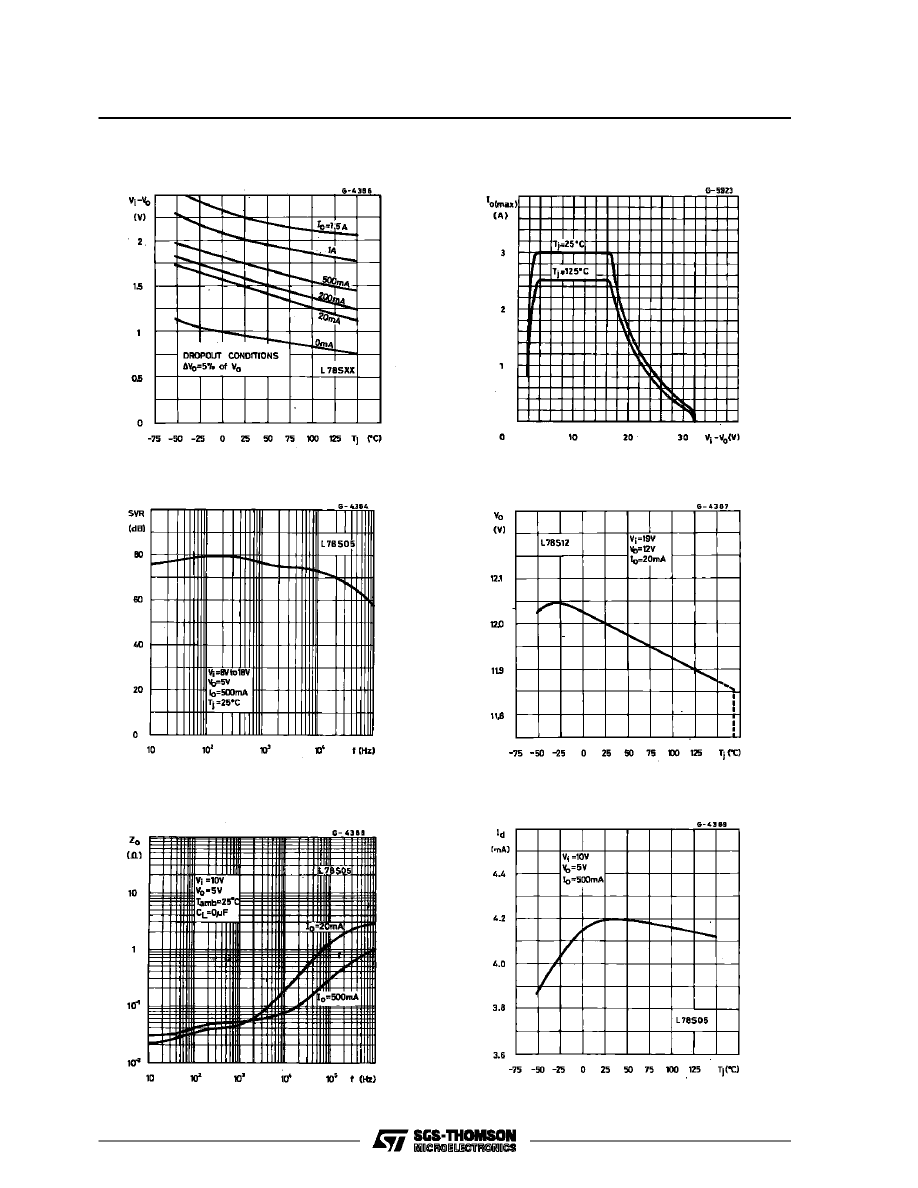
Figure 6 : Supply Voltage Rejection vs. Frequen-
cy.
Figure 7 : Output Voltage vs. Junction Tempera-
ture.
Figure 4 : Dropout Voltage vs. Junction Tempera-
ture.
Figure 5 : Peak Output Current vs. Input/Output
Differential Voltage.
Figure 8 : Output Impedance vs. Frequency.
Figure 9 : Quiescent Current vs. Junction Tempe-
rature.
L78S00 SERIES
13/21
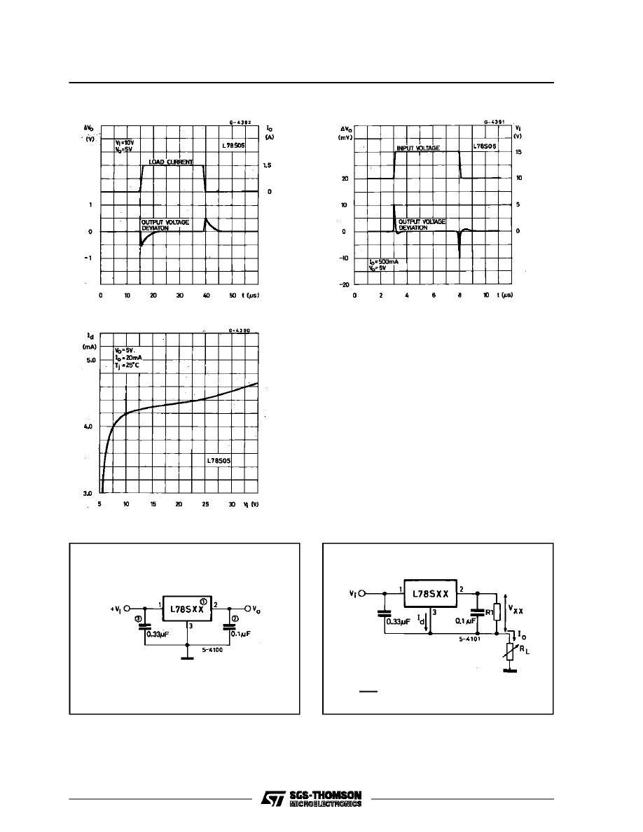
Figure 12 : Quiescent Current vs. Input Voltage.
Figure 13 : Fixed Output Regulator.
Figure 14 : Constant Current Regulator.
Figure 10 : Load Transient Response.
Figure 11 : Line Transient Response.
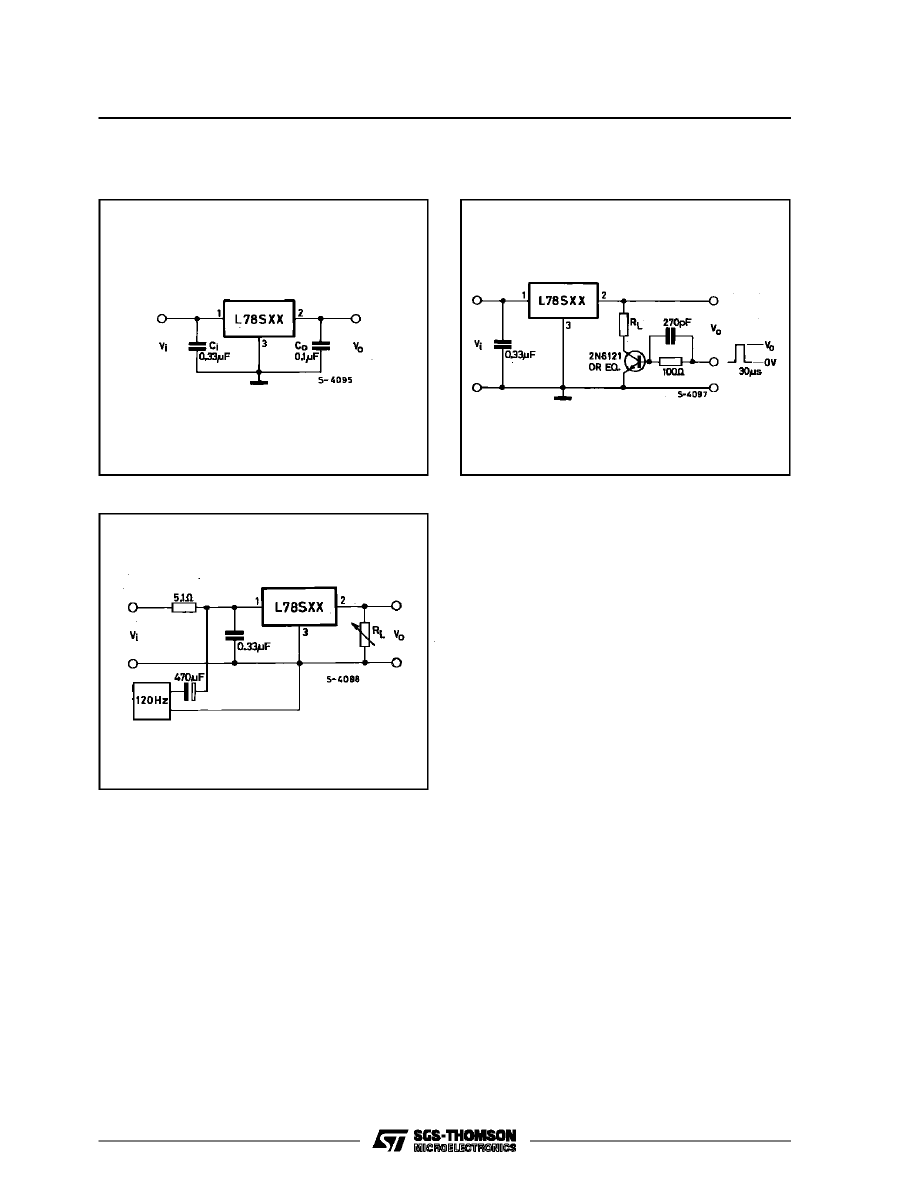
Notes : 1.
To specify an output voltage, substitute voltage
value for ” XX”.
2.
Although no output capacitor is needed for sta-
bili ty, it does improve transient response.
3.
Required if regulator is located an appreciable
dis-tance from power supply filter.
V
XX
I
O
=
+ I
d
R
1
L78S00 SERIES
14/21
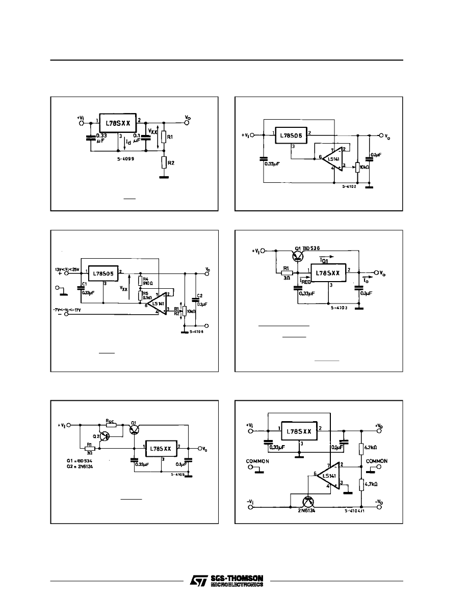
Figure 15 : Circuit for Increasing Output Voltage.
Figure 16 : Adjustable Output Regulator
(7 to 30V).
Figure 17 : 0.5 to 10V Regulator.
Figure 18 : High Current Voltage Regulator.
V
BEQ1
R
1
=
I
Q1
I
REQ
–
β
Q1
V
BEQ1
I
O
= I
REG
+ Q
1
[I
REG
–
]
R
1
R
4
V
O
= V
XX
R
1
I
R1
≥
5 I
d
R
2
V
0
= V
XX
(1 +
) + I
d
R
2
R
1
Figure 19 : High Output Current with Short Circuit
Protection.
Figure 20 : Tracking Voltage Regulator.
V
BEQ2
R
SC
=
I
SC
L78S00 SERIES
15/21
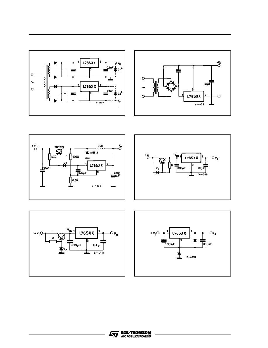
Figure 21 : Positive and Negative Regulator.
Figure 22 : Negative Output Voltage Circuit.
Figure 23 : Switching Regulator.
Figure 24 : High Input Voltage Circuit.
V
IN
= V
i
– (V
Z
+ V
BE
)
(*) D
1
and D
2
are necessary if the load is connected be-
tween + V
0
and – V
0
.
Figure 25 : High Input Voltage Circuit.
Figure 26 : High Output VoltageRegulator.
V
IN
= V
Z
- V
BE
L78S00 SERIES
16/21
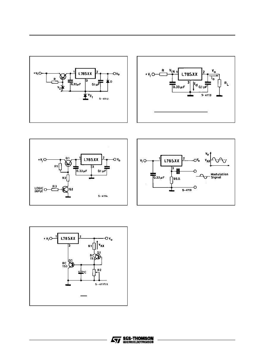
Figure 27 : High Input and Output Voltage.
Figure 28 : Reducing Power Dissipation with
Dropping Resistor.
V
O
= V
XX
+ V
Z1
V
i(min)
– V
XX
– V
DROP(max)
R =
I
O(max)
+ I
d(max)
Figure 29 : Remote Shuntdown.
Figure 30 : Power AM Modulator (unity voltage
gain, Io
≤
1A).
Note : The circuit performs well up to 100KHz.
Figure 31 : Adjustable Output Voltage with Tem-
perature Compensation.
Note :Q
2
is connected as a diode in order to compensat e
the vari ati on of the Q
1
V
BE
wi th the temper atur e. C
all ows a slow rise-t ime of the V
O
R
2
V
O
= V
XX
(1 +
) + V
BE
R
1
L78S00 SERIES
17/21
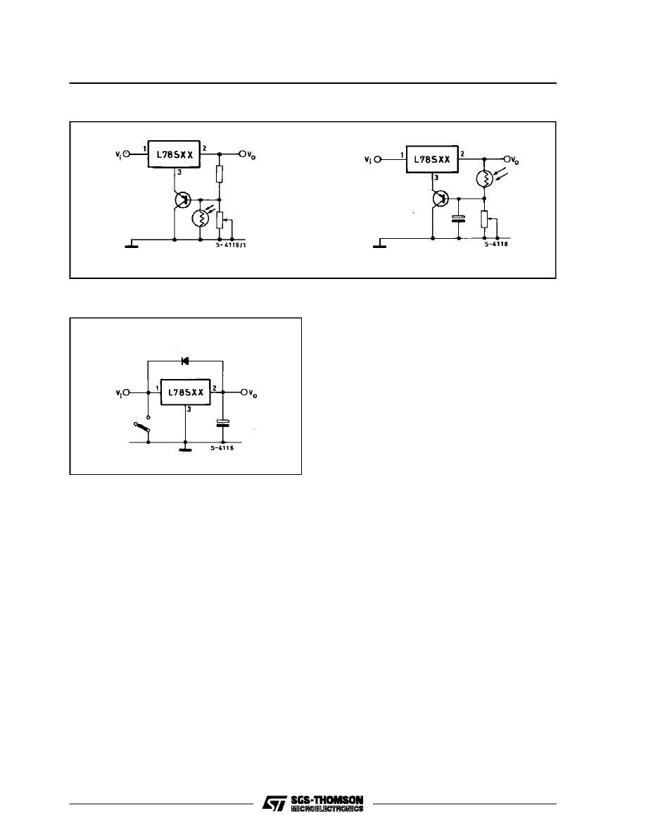
Figure 32 : Light Controllers (V
o min
= V
xx
+ V
BE
).
V
O
falls when the light goes up
V
O
rises when the light goes up
Figure 33 : Protection against Input Short-circuit
with High Capacitance Loads.
Applications with high capacitance loads and an
output voltage greater than 6 volts need an external
diode (see fig. 33) to protect the device against input
short circuit. In this case the input voltage falls
rapidly while the output voltage decreases showly.
The capacitance discharges by means of the Base-
Emitter junction of the series pass transistor in the
regulator. If the energy is sufficiently high, the tran-
sistor may be destroyed. The external diode by-
passes the current from the IC to ground.
L78S00 SERIES
18/21
DIM.
mm
inch
MIN.
TYP.
MAX.
MIN.
TYP.
MAX.
A
11.00
13.10
0.433
0.516
B
0.97
1.15
0.038
0.045
C
1.50
1.65
0.059
0.065
D
8.32
8.92
0.327
0.351
E
19.00
20.00
0.748
0.787
G
10.70
11.10
0.421
0.437
N
16.50
17.20
0.649
0.677
P
25.00
26.00
0.984
1.023
R
4.00
4.09
0.157
0.161
U
38.50
39.30
1.515
1.547
V
30.00
30.30
1.187
1.193
C
D
N
B
V
U
R
A
P
E
G
O
P003F
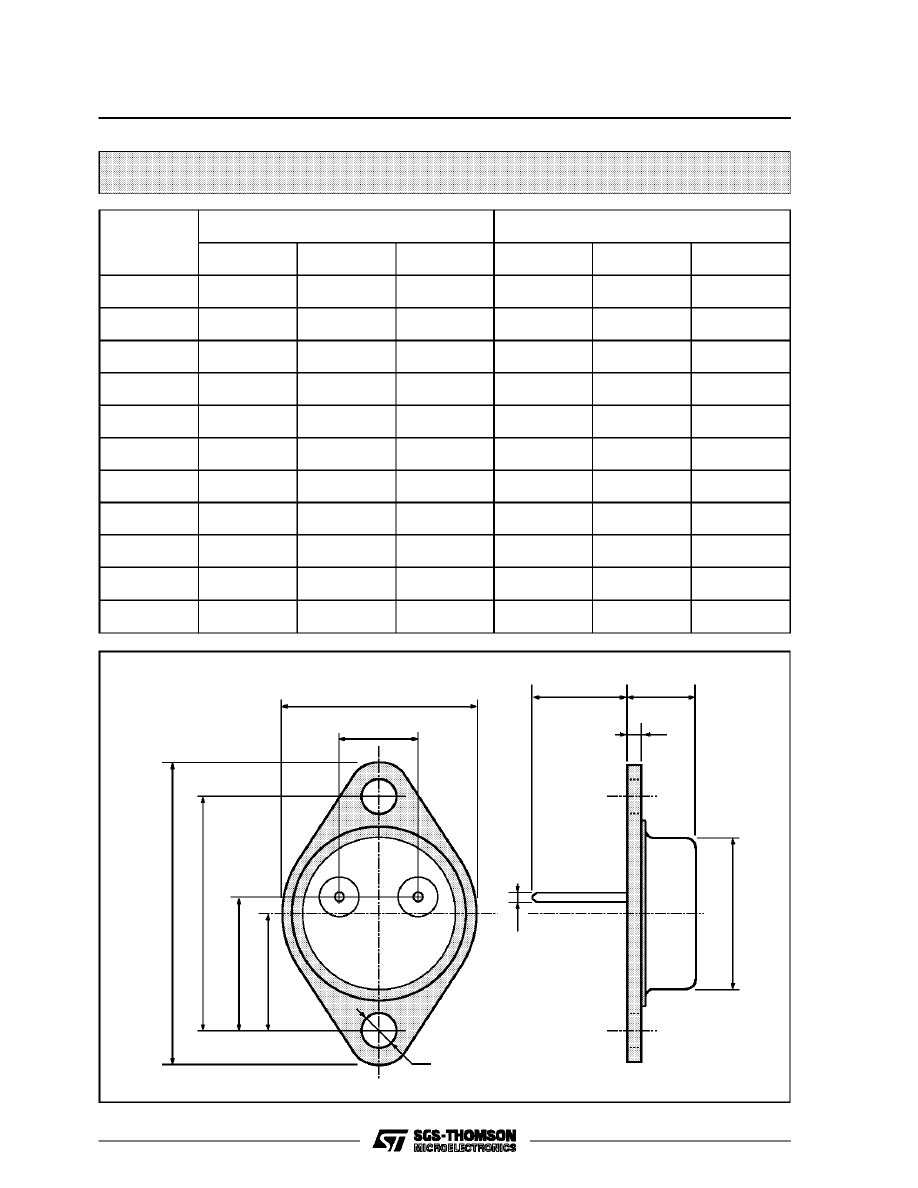
TO-3 MECHANICAL DATA
L78S00 SERIES
19/21
DIM.
mm
inch
MIN.
TYP.
MAX.
MIN.
TYP.
MAX.
A
4.40
4.60
0.173
0.181
C
1.23
1.32
0.048
0.051
D
2.40
2.72
0.094
0.107
D1
1.27
0.050
E
0.49
0.70
0.019
0.027
F
0.61
0.88
0.024
0.034
F1
1.14
1.70
0.044
0.067
F2
1.14
1.70
0.044
0.067
G
4.95
5.15
0.194
0.203
G1
2.4
2.7
0.094
0.106
H2
10.0
10.40
0.393
0.409
L2
16.4
0.645
L4
13.0
14.0
0.511
0.551
L5
2.65
2.95
0.104
0.116
L6
15.2
15.9
0.598
0.625
L7
6.2
6.6
0.244
0.260
L9
3.5
4.2
0.137
0.165
DIA.
3.75
3.85
0.147
0.151
L6
A
C
D
E
D1
F
G
L7
L2
Dia.
F1
L5
L4
H2
L9
F2
G1
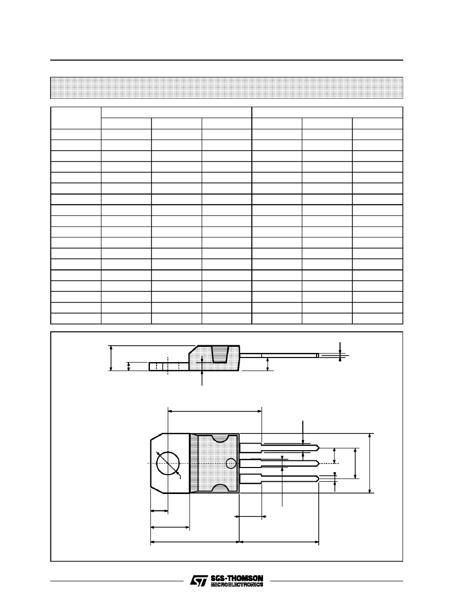
TO-220 MECHANICAL DATA
P011C
L78S00 SERIES
20/21
Information furnished is believed to be accurate and reliable. However, SGS-THOMSON Microelectronics assumes no responsability for the
consequences of use of such information nor for any infringement of patents or other rights of third parties which may results from its use. No
license is granted by implication or otherwise under any patent or patent rights of SGS-THOMSON Microelectronics. Specifications mentioned
in this publication are subject to change without notice. This publication supersedes and replaces all information previously supplied.
SGS-THOMSON Microelectronics products are not authorized for use as critical components in life support devices or systems without express
written approval of SGS-THOMSON Microelectonics.
1994 SGS-THOMSON Microelectronics - All Rights Reserved
SGS-THOMSON Microelectronics GROUP OF COMPANIES
Australia - Brazil - France - Germany - Hong Kong - Italy - Japan - Korea - Malaysia - Malta - Morocco - The Netherlands -
Singapore - Spain - Sweden - Switzerland - Taiwan - Thailand - United Kingdom - U.S.A
L78S00 SERIES
21/21
Wyszukiwarka
Podobne podstrony:
Algorytmy Genetyczne AG 3 id 61 Nieznany (2)
analiza pomoc naukowa cz1 id 61 Nieznany (2)
analiza finansowa egzamin id 61 Nieznany (2)
Power of Motivation id 379151 Nieznany
61 (2012) streszczenia id 44220 Nieznany
art 6 61 id 69346 Nieznany
FRFU 61 t2 523 id 181029 Nieznany
60,61,62 id 44165 Nieznany
61 id 44205 Nieznany
Nye Soft power id 325343 Nieznany
61 68 id 44222 Nieznany (2)
Alarm gsm id 54676 Nieznany
60 61 id 44182 Nieznany
61 4 id 44212 Nieznany
Alarm prestige amx id 54682 Nieznany (2)
61 2 id 44209 Nieznany (2)
61 (2012) streszczenia id 44220 Nieznany
Abolicja podatkowa id 50334 Nieznany (2)
4 LIDER MENEDZER id 37733 Nieznany (2)
więcej podobnych podstron