Topics Covered
Introduction
Balancing mechanisms
Application on TIG welding
Paralleling IR standard speed IGBTs
Full Bridge Inverter
Power circuit
Half-Bridge Inverter
Output inverter stages
Transient voltage and output rectifier
Multi-process welding
Advantages of paralleling IGBTs
Mounting instructions
Current and temperature unbalance
ESD and correct handling
Thermal runaway
Discrete devices approach
Conclusions
1. Introduction
A common use of IR Standard Speed IGBTs is in the output inverter stage of the AC TIG
1
welding
machines. IR has designed application specific modules and the aim of this document is to provide
information on how using them. Considerations and guidelines to connect several devices in parallel
are also provided for very high current applications.
Table 1.
IR recommended products for switching output stage of AC TIG welding machines
1
TIG, Tungsten Inert Gas, also called GTAW (Gas Tungsten Arc Welding)
A
PPLICATION
N
OTE
AN-1045
AC TIG Welding: Output Inverter Design Basics
By A. Roccaro, R. Filippo, M. Salato
www.irf.com
1
International Rectifier
•••••
233 Kansas Street El Segundo CA 90245 USA
Configuration
Part number IR IGBT Type Diode type
V
CES
(V)
I
C
@25ºC
(A)
I
C
@100ºC
(A)
Package
Single switch without
freewheeling diode
GA200SA60S
Standard Speed
- 600
200 100
SOT-227
Half bridge without
freewheeling diode
GA200HS60S
Standard Speed
- 600
380 250 IAP
Half bridge with
freewheeling diode
GA100TS60SQ Standard Speed Fast QuietIR 600 220
200
IAP
2
www.irf.com
AN1045
2. Application on TIG welding
Unlike other welding machines, TIG ones are not suited to work with magnetic-type power supplies.
These deliver an alternating current of line frequency (50Hz or 60Hz depending on geographic area)
with slow reversals that hamper reignition of the arc at next half wave; auxiliary means can provide high
frequency ionizing voltage (HF), but often the instantaneous current is too low [3]. Nowadays, this
problem is avoided by using an output inverter stage connected to a regulated dc power supply.
The output inverter stage provides an ac square-wave (rapid zero crossover) that improves ac perfor-
mance enhancing arc reignition (deionization does not occur) to the extent that HF systems are
unnecessary [3]. As HF generates abnormal high electromagnetic emission, its use could cause
interference especially in electronic equipment as radio or television (EMI).
The frequency of this ac-wave is kept low (few hundreds Hz) for intrinsic application requirements.
Two commonly used configurations of an output inverter are discussed in the following sections.
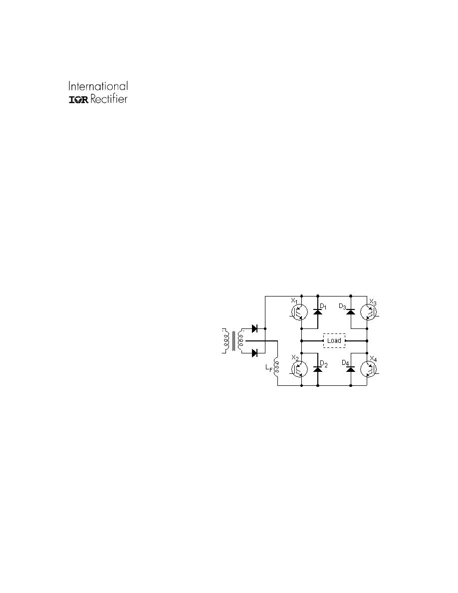
2.1 Full Bridge Inverter
Consider the full-bridge inverter output stage
shown in figure 1. Every IGBT symbol in the
picture is equivalent to one or more IGBTs con-
nected in parallel. The inverter consists of two
legs: X
1
, X
2
form leg A, while X
3
, X
4
form leg B.
Commonly, the IGBTs are arranged to switch
in pairs, (X
1
, X
4
) and (X
2
, X
3
); the IGBTs in each
pair are turned off and on simultaneously. Also,
the pairs are switched in such a way that when
one of them is in its ON state, the other is
OFF: when X
1
and X
4
are ON, X
2
and X
3
are
OFF and vice versa (although in practice this
is not always true, and it will be addressed
later). In figure 1 are also included anti-parallel protection diodes connected to the IGBTs (D
1
, D
2
, D
3
,
D
4
). The use of these diodes is highly recommended since they provide a path to the reverse current to
ensure a low, safe V
EC
.
The reverse current can be named a “reactive” current, because it would not be present with a purely
resistive load (the arc). Under some conditions the reverse current is neither present nor harmful, but
in other circumstances it is; since many times the operating conditions are totally unpredictable,
protection diodes should always be used.
Figure 1.
Simplified circuit of the Full-Bridge output
Inverter.
www.irf.com
3
AN1045
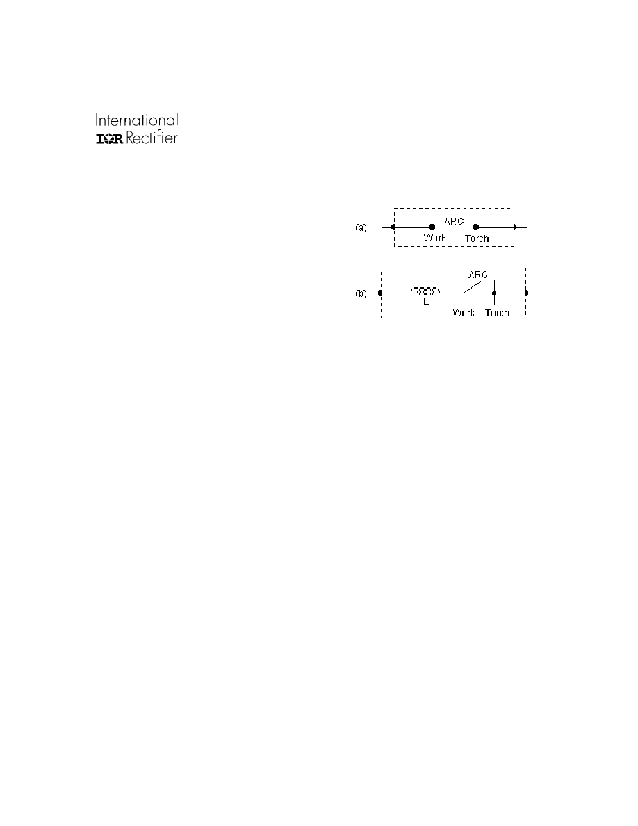
The arc just resists to the current flow and has low reac-
tive components. The real threat is the inductive compo-
nent introduced by the wires connecting the inverter out-
put to the electrode and the work piece (inductance is
proportional to cable length). Hence, an inductor in se-
ries with the arc composes a more accurate model of
the load (figure 2b). When a pair of IGBTs is ON and the
current I
L
flows through the load, energy is stored in the
stray inductance of the wires. When the inverter switches,
the current I
L
changes direction, but the inductance re-
jects this sudden change and pumps the reverse cur-
rent. If protection diodes were not present, this current
would cause undesirable under stress operation of the
IGBTs and might even lead to exceed the maximum allowed V
EC
voltage damaging the device.
Another consideration arises. All the IGBTs should not be OFF at once during switching, since the
power source feeding the inverter continuously supplies current. It follows that a pair of IGBTs should
be turned ON a time t
∆
before turning OFF the other pair; time t
∆
depends on turn-on and turn-off times
associated to the devices (normally is some hundreds of nanoseconds long).
As a result, for a finite short time, a cross-conduction of current takes place through the legs and the
IGBTs must withstand it. During this interval of time, the only harmless path for the reverse current is
through a “free-wheeling” diode and an IGBT; thus a further reason for using the diodes.
To reduce reverse current and cross conduction effects, most designers use the approach of “shaping”
the current waveform through an appropriate control of the primary inverter. It consists in reducing the
magnitude of the load current to few amperes before changing its polarity (switching the IGBTs). In this
case, relatively small clamps avoid unsafe voltage spikes during intervals in which all the IGBTs are
kept OFF. Current shaping also allows to build very accurate current profiles to optimize the welding
process.
When selecting the protection diodes, it is important to consider parameters such as the maximum
peak, average and RMS forward current, the dissipated power, the breakdown voltage, and the speed.
In most cases, the discrete diode 40EPF06 can be a good choice: it has 40A of average forward
current, its maximum peak reverse voltage is 600V, it has an ultra soft recovery, and it is optimized for
short reverse recovery time and low forward voltage. It also ensures stable and reliable operation in
severe temperature and power cycling conditions.
Figure 2.
Models of the load: (a) basic and
(b) more accurate
4
www.irf.com
AN1045
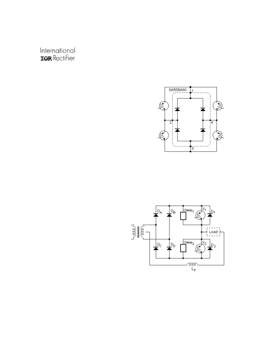
Another valid option can be the rectifier bridge SA55BA60
2
that contains, in one single device, all four freewheeling di-
odes arranged to allow a direct connection to “H-Bridge” in-
verters (figure 3). It has 55A of average forward current, its
maximum peak reverse voltage is 600V and it has fast recov-
ery time. Also, the SOT-227 package with an electrically iso-
lated base plate and its bridge configuration allow common
heat sinks usage, simplified mechanical designs, and com-
pact and rapid assemblies.
Where the “current-shaping” technique results in very low
switching current, even smaller diodes can be used, such as
the 10ETF06, which has the same characteristics of the
40EPF06 except for a lower average forward current of 10A.
2.2 Half-Bridge Inverter
Consider now the inverter circuit of figure 4. The number of diodes in the output rectifier is doubled, in
respect to the “Full-Bridge” configuration, but the number of equivalent IGBTs is now a half. This circuit
usually leads to system simplifications and cost savings.
The IGBTs are switched in such a way that when one of them is in ON, the other is OFF. During the
positive half wave, X
1
is ON and X
2
is OFF thus
D
A
and D
B
work as output rectifier while D
C
and
D
D
are OFF. Vice versa, during the negative
half wave, X
2
is ON and X
1
is OFF, thus D
C
and
D
D
work as output rectifier while D
A
and D
B
are
OFF.
The following considerations arise:
•
In this circuit, cross conduction must be
accurately avoided. X
1
and X
2
must never
be ON at the same time. This is accom-
plished by switching X
2
ON a time t
∆
after
X
1
is switched OFF. Again, this blanking
time depends on turn-on and turn-off times
associated to the devices.
Figure 3.
Application and pinout of
SA55BA60 in “H-Bridge”
inverters (load not shown)
Figure 4.
Simplified circuit of the Half-Bridge output
inverter
2
Now available on request as S1223

www.irf.com
5
AN1045
•
There is no freewheeling current. D
1
and D
2
are protection diodes which ensure that V
EC
is always well
below the safety limit, in particular during switching transients. Very low current diodes can therefore
be used, provided they are fast enough. The 8ETH06 or the 10ETF06 suit well to the purpose.
•
During the blanking time, the energy stored in the load and in the filter inductor L
F
has to be
somehow dissipated prior of the current reversal. RC-Diode clamps are often used. Sometimes,
the IGBT which is switching OFF is used in linearity as part of the clamp. Caution and accurate
design verification must be performed in such a case, since the IGBTs are designed for switching
operation and are not intended for linear use. The energy to be dissipated in the clamp can be
made very small by implementing the current shaping technique, resulting in additional cost sav-
ing.
2.3 Transient voltage and output rectifier
In most cases open circuit output voltages are around 80V, which is considerably higher than the arc
voltage. However, the transient voltage peaks might represent an issue, and for this reason the IGBTs
used must have a high enough collector-emitter breakdown voltage.
When an IGBT is turned off, it dissipates the stored energy in the circuit stray inductance, causing a
voltage overshoot across the device. The magnitude of this transient voltage is mostly determined by
the gate drive circuit, and is proportional to the stray inductance, the magnitude of the switched current
and its rate of fall at turn-off. Hence, performing the shaping of the load current reduces overshoots.
Semiconductor devices having blocking voltages of at least 400V are normally used. For the output
rectification, IR offers a wide series of 400V Ultrafast Recovery Epitaxial Diodes which provide a safe
margin against transient voltages. In particular, for a full modular approach, IR has developed the
UFB200FA40 which provides two independent, insulated diodes in SOT-227 package. More modules
can be paralleled together to reach higher current. The IRUD360CW40 (containing two common-
cathode diodes in non-insulated TO-244 package) is another interesting choice for very high current
application whenever the insulation can be easily provided by the designer.
IR IGBT modules for output inverters can instead withstand at least 600V of collector-emitter voltage
(V
CES
) while in the OFF state.
3. Advantages of paralleling IGBTs
The main reason to parallel IGBTs is to increment the driven current. Sometimes, the only way to
achieve the desired current level is by using similar devices in parallel.
Paralleling helps to reduce the conduction losses and the junction to ambient thermal resistance.
6
www.irf.com
AN1045
However, switching losses remain the same, or may even increase due to non-symmetrical layout or
high current unbalance. The maximum utilization will only be achieved in the case of ideal static and
dynamic operation. Therefore, symmetry conditions are of significant importance for parallel connec-
tions.
To successfully parallel IGBTs, some items must be considered: the current and temperature unbal-
ance between devices (due to the IGBTs themselves), and gate circuitry and layout (which come up
due to external circuitry).
4. Issues and guidelines on paralleling: Static considerations
4.1 Current and temperature unbalance
When paralleling any power semiconductors, the first issue that comes to mind is how well they share the
total current. Given several IGBTs, the V
CE(on)
for different current levels will be slightly different. When
these IGBTs are operated in parallel, the V
CE(on)
across the devices is forced to be the same. Thus, for a
given load current, one IGBT will carry more current than the others, creating an unbalance that at lower
currents can be up to 100% (one IGBT carries all current). However, as long as the current remains below
the maximum specified on the data sheet, current unbalance is not critically important [1].
IR TIG modules are designed to have output characteristics with a very narrow spread, favoring current
balance and easing paralleling since, normally,
screening is not necessary.
However, generally speaking, semiconductors are tem-
perature limited rather than current limited, so the
real issue is whether or not one of the devices ap-
proaches the rated junction temperature and how
closely they are matched in junction temperature in
order to avoid the thermal runaway and obtain the
maximum system efficiency. The device carrying
more current has a higher junction temperature that
may exceed the maximum rated value: This factor
should be the designer primary concern [1].
4.2 Thermal runaway
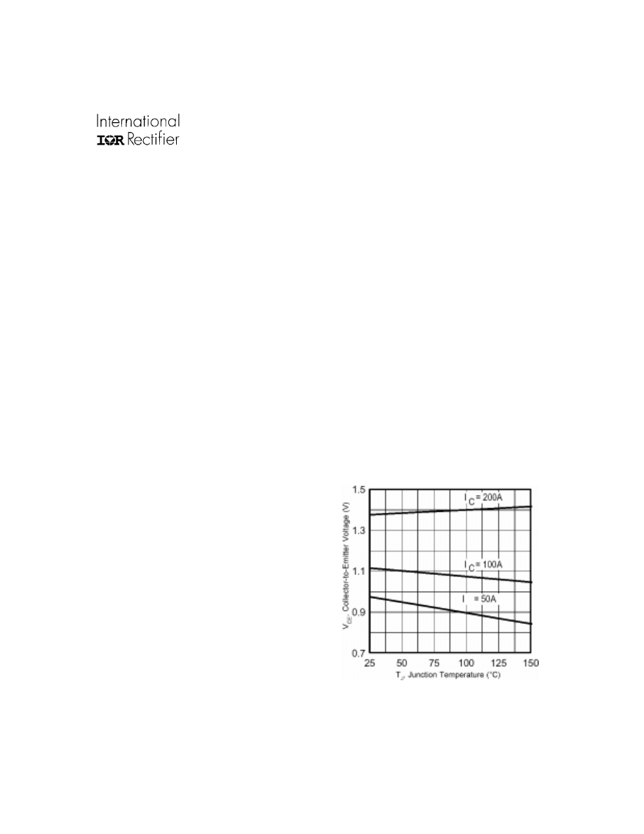
The temperature dependence of the output charac-
teristics is low in IR Standard Speed IGBTs and the
temperature dependence of the voltage drop is differ-
ent at different current levels.
Figure 5.
V
CE(on)
voltage drop vs. temperature
in the GA100TS60SQ
www.irf.com
7
AN1045
In paralleled IGBTs, the one with the lower saturation characteristic conducts the major current share.
Therefore it will have higher forward and switching losses and when operation starts its junction tem-
perature will increase. In this respect, the temperature coefficient (TC) of the saturation voltage is of
decisive importance. If positive (the saturation voltage rises together with the temperature), the con-
duction characteristic degenerates (its impedance increases) and a share of the current will be shifted
to the transistors that carried less current initially, so that the current will be evenly distributed over the
paralleled transistors. If TC is negative the device carrying more current lowers its impedance, thus
resulting in further current increase, and so on until a thermal failure occurs. This is why the power
semiconductors with a positive TC are preferred in parallel connections.
The IGBT, being a combination of a power MOSFET and a BJT, cannot be simply described as having
either negative or positive temperature coefficient. The temperature coefficient is dependent on the
technology used in the IGBT design. Even within the same technology, it changes depending on the
current density. As an example, in the GA100TS60SQ the TC is negative for low currents and positive
for high currents (see figure 5). However, in IR Standard Speed technology, even when the device
operates in the negative TC zone, thermal runaway does not occur, as will be discussed in section 4.3.
4.3 Balancing mechanisms
There are three factors that help to reduce the
current unbalance: good thermal coupling, differ-
ent TC of the devices, and high currents [1].
The first factor that keeps the unbalance in check
is the thermal feedback between the junctions.
The one with higher power dissipation increases
the sink temperature and consequently the junc-
tion temperature of the others by an amount that
is inversely proportional to the thermal resistance
between the junctions. If the thermal coupling
between the dice is tight, the temperature differ-
ential cannot be significant.
Using a common heat sink establishes a thermal
coupling between the dice that limits their tempera-
ture differential, remaining in the order of few de-
grees. It is also very important that the devices are
mounted correctly (see paragraph 6.3). The use of
separate heat sinks, instead, would cause large
current unbalance and very significant temperature differentials, hence, their use should be avoided.
1
10
100
1000
0.5
1.0
1 .5
2.0
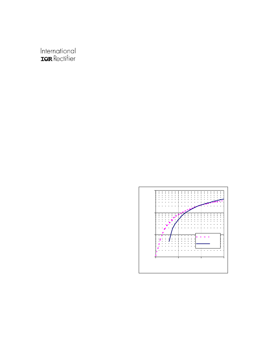
Vce, C ollect or-em it t er volt age (V)
Ic
, C
o
ll
e
c
to
r-
e
m
it
te
r c
u
rr
e
n
t (
A
)
1 5 0 ºC
2 5 ºC
Figure 6.
Typical output characteristic of the
GA200SA60S
8
www.irf.com
AN1045
The second factor that reduces the current unbalance is the different TC of the voltage drops. Even if it
is negative for all the devices, the IGBT carrying less current has a lower TC (in other words, it has a
higher absolute value of TC, as shown in fig. 5). As temperature increases, voltage drop of the major
carrier changes slightly; while voltage drop of the IGBT that was carrying little current comes down
significantly, forcing an increment of conduction, thereby closing the gap in current, as well as tem-
perature. If the temperature differential is kept low, an increase in temperature reduces the current
unbalance.
Third balancing mechanism: As the collector current increases, the voltage drop of IGBTs converges
toward a common value independent of the junction temperature (figure 6). This reduces the unbalance
at higher currents. The junction temperature increases together with the current, and this results in
further reduction of the unbalance.
4.4 Paralleling IR Standard Speed IGBTs
To ensure parallel operation of IGBTs, all condi-
tions mentioned above in paragraphs 2, 3 and 4
must be taken into account, especially the use
of a common heat sink.
Yet, even if all those conditions are met, optimal
performance is not guaranteed: Current distribu-
tion depends on the tolerances of output charac-
teristics. To reduce unbalance as much as pos-
sible, matched devices should be used. Several
methods exist to match devices, and the choice
could depend on operation mode (switching or
not), impact of lifetime killing on the behavior of
the devices, and others.
The High-Speed/Low-V
CE(on)
trade-off In the fabri-
cation process of IGBTs, is of relevance, as rep-
resented in the example of figure 7. Lower speed devices give superior conduction efficiency first, and
less deviation of the V
CE(ON)
distribution then. Such a narrow distribution favors current balance when
more devices are paralleled together. This explains why IR TIG products are easier to be paralleled (do
not require screening), providing very high output currents in heavy-duty operation.
Furthermore, in IR Standard Speed devices the TC increases with current and becomes positive at a
certain
3
current (figure 5), this guarantees operation without thermal runaway.
0
1
2
3
4
1.2
1 .4
1.6
1.8
2.0
2.2
Vce(on) (V )
Eo
ff
+
E
o
n
(
m
J
)
St an da r d
sp eed (S)
Fast (F)
U lt r a-Fa st
( U)
W ar p
( W )
Figure 7.
Example of E
tot
vs. V
CE(on)
trend
(Size 3, Gen. 4 IGBT @ I
C
=12A)
www.irf.com
9
AN1045
3
200A for the GA100TS60SQ and GA200SA60S; 280A for the GA200HS60S
0 .3
0 .3
0 .4
0 .2
5 .3
6 .9
8 .0
4 .4
0
2
4
6
8
10
0
100
200
300
T ot al current (A )
C
u
rr
e
nt
un
ba
la
nc
e
(
%
)
Sim ilar devices
D ifferent devices
G A 100T S60SQ
b)
0 .2
0 .1
0 .1
4 .5
4 .4
4 .5
4 .4
0
1
2
3
4
5
50
60
70
80
C ase t emp erat ure (°C )
C
u
rr
e
nt
un
ba
la
nc
e
(
%
)
Similar devices
D ifferent devices
It o t = 2 9 5 A
It o t = 3 0 3 A
It o t = 3 0 6 A
It o t = 2 9 2 A
__
__
__
__
__
__
__
_
G A 100T S60SQ
__
__
a)
c)
0.90
0.92
0.94
0.96
0.98
1.00
50
60
70
80
C ase t em p erat ure (°C )
N
o
rm
al
is
ed
v
a
lu
es
T o t al curren t
(1 .0 0 = 3 0 6 A)
Curren t un balan ce
(1 .0 0 = 4 .4 9 %)
D ifferent devices
G A 100T S60SQ
Figures 8a, b and c.
Operation of two GA100TS60SQ connected in parallel to a DC power supply

10
www.irf.com
AN1045
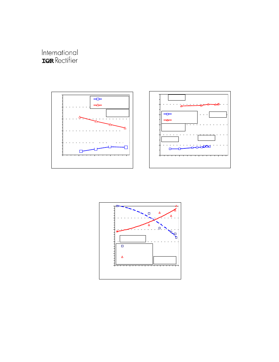
The charts in figure 8 show how all the factors mentioned above influence the current unbalance when
two GA100TS60SQ are connected in parallel to a DC power supply. The modules measured are the
pair of most “similar” and most “different” devices, selected from several devices of three different lots,
comparing the values of V
CE(on)
at different currents and at different temperatures.
Fig. 8a shows how increasing the current decreases the current unbalance. When current in each
module is 100A (that is, total current 200A), in the worst case (different devices), the current
unbalance is about 5%, while is below 0.5% in the similar devices.
The charts in figure 8b and 8c are correlated and are made with the results of the same measure-
ments. They show the change of the current unbalance with the temperature. The temperature depen-
dence of the modules is minimal. The unbalance is nearly constant even when devices operate in the
negative TC zone and thermal runaway not occurs due to a good thermal coupling and different TC of
the voltage drops. Changes in unbalance are mainly due to the decrease of the total current.
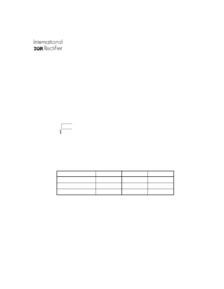
The same measurements were carried out using selecting 4 modules GA200HS60S from several
devices of different lots. The results are shown in the charts of figure 9. It can be seen how what
concluded previously for the GA100TS60SQ applies equally well: increasing current decreases cur-
rent unbalance (figure 9a); the temperature dependence of the current unbalance is minimal (figure 9b);
changes in the unbalance are mainly due to the decrease of total current (figure 9c).
These results confirm how the IR modules are well suited to work in parallel, even if devices from
different lots are used.
www.irf.com
11
AN1045
c)
0.90
0.92
0.94
0.96
0.98
1.00
50
55
60
65
70
C ase T emp erat ure (°C )
N
o
rm
a
lis
e
d
v
a
lu
e
s
T o t al curren t
(1 .0 = 3 1 9 A )
Curren t un balan ce
(1 .0 = 5 .1 %)
D ifferent devices
G A 200H S60S
Figures 9a, b and c.
Operation of two GA200HS60S connected in parallel to a DC power supply
b)
0 .6
0 .7
0 .8
0 .9
5 .0
4 .8
4 .9
5 .0
0
1
2
3
4
5
6
40
50
60
70
C ase t emp erat ure (°C )
C
u
rr
e
nt
un
ba
la
n
c
e
(
%
)
Similar devices
D ifferent devices
It o t = 2 9 3 A
It o t = 3 0 8 A
It o t = 3 1 9 A
It o t = 3 0 2 A
__
_
__
__
__
__
__
_
G A 200H S60S
0 . 6
1 .0
1 .3
1 .3
4 . 5
5 . 0
5 . 6
6 .3
0
2
4
6
8
10
0
100
200
30 0
400
T ot al curren t [A ]
C
u
rr
e
n
t unba
la
n
ce
[
%
]
Similar devices
D ifferent devices
G A 200H S60S
a)
12
www.irf.com
AN1045
Device part number
L
S
(nH)
C
ies
(pF)
Package
GA200SA60S 20 16250
SOT-227
GA100TS60SQ 120 16250
Int-A-Pak
GA200HS60S 90 32500
Int-A-Pak
Table 2.
Reference table used to calculate the minimum value of R
G
5. Issues and guidelines on paralleling: Dynamic considerations
5.1 Drive circuit
The input capacitance of the IGBT, whose gate is essentially identical to that of the MOSFET [2], and
the inductance of the gate driving circuit form together a LC loop that may cause undesired and unsafe
oscillations. To eliminate the risk of oscillations, some recommendations should be followed:
•
Use of individual gate resistors located physically close to the gate lead of the device. Impedance
deviations of the driver circuits should be avoided. An approximated value of this resistance may be
calculated through the following formula:
The value of L
tot
is the sum of two components: the first is the parasitic inductance of the PCB tracks
and the wires used to connect the gate drive circuit to the module; the second, named L
S
, includes the
internal connections of the module. The values of L
S
and C
ies
for each device are shown in table 2 (C
ies
is also reported in datasheets). The value of L
S
is calculated with measurements, FEM and BEM
simulations (Finite Elements Method and Boundary Elements Method).
•
Twist or run on parallel tracks the gate lead and the gate return lead to minimize gate emitter loop
inductance.
•
Ensure that the gate of the IGBT is looking into a stiff (voltage) source with as little impedance as
practical. This advice applies equally well to both paralleled and single device designs.
•
Do not place Zener diodes or Transient Voltage Suppressors directly between gate and emitter. If over
voltage protection is required on the gate, place the Zener diodes on the driver side of the gate resistor(s).
ies
tot
G
C
2
L
2
R
⋅
⋅
≥
where R
G
: gate resistance
L
tot
: gate emitter (drive circuit) loop inductance
C
ies
: input capacitance
www.irf.com
13
AN1045
Figure 10.
Parallel connection of two IGBT and
example of difference in transient
voltage
•
Do not place capacitors directly gate to emitter to control switching times, instead increase the gate
resistor. The capacitors may cause oscillations and slow down switching, which increases the dynamic
unbalance between devices.
5.2 Power circuit
First of all, it is very important to state that all the threats issue associated with the dynamic behavior
are dramatically reduced and even eliminated through the output current shaping technique explained
earlier. Anyway, for completeness, some hints about switching of paralleled devices are given in this
section; for a deeper analysis of switching operation of paralleled IGBTs refer to application notes AN-990.
Generally speaking, voltage equality is ensured by the fact that the devices are in parallel. However,
under transient conditions voltage differentials can appear across the devices, due to di/dt effects in
unequalized stray inductances. If the overshoots at turn-off do not violate the ratings of the IGBT, the
difference in the turn-off losses is negligible [1].
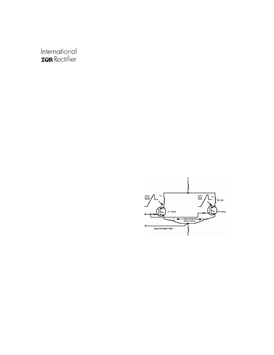
Yet, the impact of the common emitter induc-
tance on switching is far from negligible. The
IGBT with lower common emitter inductance
turns off before the others, which are left to
shoulder the entire load current during the turn-
off transient. This will increment the difference
in power dissipation between devices, leading
to an increment in junction temperature and
thermal runaway, at worst. It follows that
switch mode operation of paralleled IGBTs
should not be undertaken unless the common
emitter inductances are matched in value.
It is also important that stray components are
minimized by a tight layout and equalized by
symmetrical position of components and rout-
ing of connections. In any case, IR modules
are designed looking after to minimize the in-
ductance of the internal connections.
In practical applications the IGBTs could be operated at some frequency and losses of the devices
would have a switching component proportional to the operating frequency. The switching losses
depend on junction temperature and load current [2].

14
www.irf.com
AN1045
The IGBT carrying more current will have higher switching losses, as well as higher conduction losses.
However, the switching frequency helps bringing balanced operation, due to different TC of voltage
drop. When the power losses increase the junction temperature, the unbalance is reduced and the
rate of unbalance reduction increases with frequency [1].
If the RMS value of the output current is kept constant, a reduction in duty cycle reduces the current
unbalance. This is due to the third balancing mechanism, because to generate the same output
current with a lower duty cycle a higher peak current is necessary.
6. Using IR products
IR application specific products for AC TIG output inverter stages are shown in table 1. Below are
summarized some advantages of these IR products. Some hints about discrete IGTBs for the same
application are also given.
6.1. Output inverter stages
The TIG welding machines have operation frequencies as low as few hundreds Hz. The use of fast
switching devices, hence, is not recommended, since they have greater conduction losses. Slower, IR
Standard Speed devices are better suited for this application.
The key rating to calculate conduction losses is V
CE(on)
. The IR TIG switch modules are designed to
have the lowest-available V
CE(on)
and their use allows to achieve a more efficient circuit. The very narrow
distribution of V
CE(on)
simplify the use of IR TIG products in parallel (do not require screening), providing
very high output currents in heavy-duty operation
The value of 600V for collector-emitter breakdown voltage (V
(BR)CES
) provides a very safe margin against
transient voltages.
6.2 Multi-process welding
Besides driving high AC or pulsed DC current (typical of TIG welding machines), the IR switch modules
are also designed to drive high continuous currents: continuous collector current can be as high as
50% maximum collector pulsed current. This characteristic makes TIG family useful for multi-process
welding machines, where the output stage needs to drive current in both pulsed and continuous
modes. It is also very useful when considering effects of cross-conduction in switching operation,
since a high current pulse through the devices will be harmless.

www.irf.com
15
AN1045
6.3 Mounting instructions
For proper mounting and exchanger surface preparation the following procedure is recommended.
Heat sink Preparation
The contact surface of the heat sink must be flat, with a recommended tolerance of <0.03mm (1.18
mil) and a leveling depth of <0.02mm (0.79 mil), according to DIN/ISO 1302. In general, a milled or
machined surface is satisfactory if prepared with tools in good working condition. The heat sink mount-
ing surface must be clean, with no dirt, corrosion, or surface oxides.
Visual Inspection
Inspect the module to insure that the contact surface of the base is clean, that there are no lumps or
bulges on the base plate that could damage the base or reduce heat transfer across the surfaces.
Thermal Compound
Coat uniformly the heat sink mounting surfaces and power module base plate with a good quality
thermal compound (a small rubber roller can be used). A guide for choosing the right thermal com-
pound is in IR application notes AN-1012.
Apply uniform pressure on the package to force the compound to spread over the entire contact area.
If the layer of the compound is too thick then the thermal resistance will be increased. To determine the
correct amount of the compound for a particular application a series of experiments should be per-
formed. When the quantity is correct a very small amount of the compound should appear around the
perimeter of the device as it is slowly torqued to the heat sink.
Module Fastening
Bolt the module to the heat sink using the two fixing holes. The recommended torque (reported in datasheets)
is 1.3Nm for the SOT-227 and 4Nm for the IAP. An even amount of torque should be applied for each
individual mounting screw. A torque wrench, accurate in the specified range, must be used for mounting
the module, in order to achieve optimum results. The mounting screws must be tightened in sequence.
The first mounting screw should be tightened to one third of the maximum torque; the second screw
should then be tightened to the same torque. Full tightening of both screws can then be completed.
After a period of about 3 hours, check the torque with a final tightening in opposite sequence to allow
the spread of the compound.
Electrical Connection
Tight the screws to the power terminals avoiding any pressure on the module. The maximum torque is
reported on the datasheets. For the SOT-227, the M4 screws should be used with lock washers
(included with the packages).

16
www.irf.com
AN1045
6.4 ESD and correct handling
All IGBTs are sensitive to ESD (Electro Static Discharge) and is important to take appropriate precau-
tions when handling them.
IR modules are packaged and shipped following standards to ensure protection against ESD. In the
same way, care must be taken when using and manipulating the devices. The workplaces and the staff
should be specially prepared with conductive tables, ground connections, wrist strap, etc.
The SOT-227 modules are provided in conductive plastic tubes, while the Int-A-Pak modules come
with their terminals short-circuited by conductive foam.
For more information about ESD and its threats also refer to IR application notes AN-955.
6.5 Discrete devices approach
So far, only circuits based on IGBT modules have been considered, since the module approach gives
benefits in terms of ease of assembly, high current, and compactness of the resulting equipment.
However, in certain cases, circuits based on discrete IGBTs may be still preferred. That is usually due
to low current welding machines requirements, or to designer habits and existing manufacturing tools
and operators skills. In such cases, IR provides a complete line of discrete Standard Speed IGBTs,
with different current ratings and in different package styles, including TO-220, TO-247 and SMD
packages.
Of course, the benefits of the IR Standard Speed technology are still valid. The easy of paralleling can
be helpful to reach higher currents.
In the same way, for the the output rectifier IR offers a complete series of Ultrafast recovery rectifiers in
a wide choice of discrete packages.
Particular care should be taken for obtaining low case-to-junction thermal resistance, specially when
the devices need to be insulated from the heat sink. Refer to IR application notes AN-1012 “Mounting
Considerations for International Rectifier’s Power Semiconductor Packages” and AN-1023 “Surface
Mounting of Larger Devices” for proper mounting guidelines.

www.irf.com
17
AN1045
Configuration Part
number
V
CES
(V)
I
C
@25ºC
(A)
I
C
@100ºC
(A)
Package
IRG4PC50S TO-247AC
Single switch
without FW diode
IRG4PC50S-P
600 70
41
SM TO-247
IRG4PC40S TO-247AC
Single switch
without FW diode
IRG4BC40S
600 60
31
TO-220AB
IRG4PC30S TO-247AC
IRG4BC30S TO-220AB
Single switch
without FW diode
IRG4BC30S-S
600 34
18
D2-Pak
Single switch
without FW diode
IRG4IBC30S 600
23.5 13
TO-220
FullPak
Table 3.
Discrete IR Standard Speed for switching output stage of TIG welding machines
7. Conclusion
The TIG welding machines have low operating frequencies (few hundreds of Hz) and high DC or AC
currents (up to 500A). IR Standard Speed IGBTs are very well suited to work under these conditions.
Another important item to consider is the use of anti-parallel diodes for protecting the IGBTs and the
power source. The discrete diode IR 40EPF06 or the rectifier bridge SA55BA60 represent a valid
option. If the current waveform is shaped (the magnitude of current is reduced to few amperes before
changing its polarity) and/or the Half-Bridge configuration is used, the diode 10ETF06 or 8ETH06 could
be a better alternative. Shaping the current waveform helps to reduce voltage overshoots and reduces
switching losses, improving switching operation.
IR modules help to achieve a more efficient circuit, since they have the lowest-available V
CE(on)
. They
also provide a very safe margin against transient voltages with 600V for V
(BR)CES
. High current driving
capability in both AC and DC modes makes the TIG family useful for multi-process welding machines.
To improve the current capability, IR modules can be paralleled, since they will operate with very low
current unbalance. Thanks to the manufacturing process, normally there is no need for screening, thus
easing parallel connection. Their temperature dependence is minimal. The modules have an electri-
cally isolated base plate that eases handling.

18
www.irf.com
AN1045
WORLD HEADQUARTERS:
233 Kansas St., El Segundo, California 90245 Tel: (310) 252-7105
http://www.irf.com/ Data and specifications subject to change without notice. 2/10/2003
Increasing current drive helps to reduce unbalance in paralleled IR Standard Speed IGBTs: V
CE(on)
converges towards a common value independent of the junction temperature and the TC increases
with the current, and, becomes positive at 50% of maximum current. The use of a separate heatsink in
paralleled devices must be avoided. Proper mounting of devices limits junction temperature differential
keeping a good balance.
When designing the drive circuit is important to use individual gate resistors placed close to gate
terminals and twist or run in parallel tracks the gate leads to minimize gate emitter loop inductance.
The use of Zener diodes, TVS, and capacitors should be avoided.
IR wide choice of IGBTs and output diodes both in module and discrete packages can satisfy almost
all multi-process welding machine design needs.
8. References
[1]
International Rectifier, IR AN-990 “Application characterization of IGBTs”.
[2]
Ned Mohan, Tore Undeland, Willliams P. Robbins. “Power electronics, converters, applications
and design”. 2nd edition. John Wiley & Sons, Inc. New York 1995 (USA)
[3]
Tomsic M.J, N. Crump and others “The welding handbook: Welding processes”. Volume 2. 8th
edition. American Welding Society. Miami (USA). pp 2-29, 73-80.
[4]
International Rectifier, IR AN-955 “Protecting IGBTs and MOSFETs from ESD”.
[5]
International Rectifier, AN-1012 “Mounting Considerations for International Rectifier’s Power Semi-
conductor Packages”
[6]
International Rectifier, AN-1023 “Surface Mounting of Larger Devices”.
Wyszukiwarka
Podobne podstrony:
How to Design Programs An Introduction to Computing and Programming Matthias Felleisen
Design of an Audio Frequency Vacuum Tube Amplifier Brad Bryant 2000
TIG welding48 143289
Free How to do TIG Welding Guide
Design of an Artificial Immune System as a Novel Anomaly Detector for Combating Financial Fraud in t
(1 1)Fully Digital, Vector Controlled Pwm Vsi Fed Ac Drives With An Inverter Dead Time Compensation
Performance Improvements in an arc welding power supply based on resonant inverters (1)
(1 1)Fully Digital, Vector Controlled Pwm Vsi Fed Ac Drives With An Inverter Dead Time Compensation
(1 1)Fully Digital, Vector Controlled Pwm Vsi Fed Ac Drives With An Inverter Dead Time Compensation
Inverter controller for HVDC systems connected to weak AC sy
A Study Of Series Resonant Dc Ac Inverter
An Optically Isolated Hv Igbt Based Mega Watt Cascade Inverter Building Block For Der Applications
Design of a 10 kW Inverter for a Fuel Cell
How an inverter fits into your solar electric system By Jo
Modified PWM Control for the DC AC Inverter With a Non Constant Voltage Source
12V DC to 230V AC Inverter, 12v 230v inv
więcej podobnych podstron