
DOI: 10.1126/science.1167130
, 610 (2009);
323
Science
et al.
D. C. Elias,
Hydrogenation: Evidence for Graphane
Control of Graphene's Properties by Reversible
www.sciencemag.org (this information is current as of July 10, 2009 ):
The following resources related to this article are available online at
http://www.sciencemag.org/cgi/content/full/323/5914/610
version of this article at:
including high-resolution figures, can be found in the online
Updated information and services,
http://www.sciencemag.org/cgi/content/full/323/5914/610/DC1
can be found at:
Supporting Online Material
found at:
can be
related to this article
A list of selected additional articles on the Science Web sites
http://www.sciencemag.org/cgi/content/full/323/5914/610#related-content
http://www.sciencemag.org/cgi/content/full/323/5914/610#otherarticles
, 1 of which can be accessed for free:
cites 30 articles
This article
14 article(s) on the ISI Web of Science.
cited by
This article has been
http://www.sciencemag.org/cgi/content/full/323/5914/610#otherarticles
1 articles hosted by HighWire Press; see:
cited by
This article has been
http://www.sciencemag.org/cgi/collection/mat_sci
Materials Science
:
subject collections
This article appears in the following
http://www.sciencemag.org/about/permissions.dtl
in whole or in part can be found at:
this article
permission to reproduce
of this article or about obtaining
reprints
Information about obtaining
registered trademark of AAAS.
is a
Science
2009 by the American Association for the Advancement of Science; all rights reserved. The title
Copyright
American Association for the Advancement of Science, 1200 New York Avenue NW, Washington, DC 20005.
(print ISSN 0036-8075; online ISSN 1095-9203) is published weekly, except the last week in December, by the
Science
on July 10, 2009
Downloaded from

was estimated to be 5 × 10
16
m
−2
on the basis of
the spacing between the neighboring partials and
l. This is two orders of magnitude higher than
that of the preexisting dislocations and the lattice
dislocations stored in the coarse twins. Such a
finding suggests that decreasing the twin thick-
ness facilitates the dislocation-TB interactions and
affords more room for storage of dislocations,
which sustain more pronounced strain hardening
in the nt-Cu (26, 27).
These observations suggest that the strain-
hardening behavior of nt-Cu samples is governed
by two competing processes: dislocation-dislocation
interaction hardening in coarse twins, and dislocation-
TB interaction hardening in fine twins. With a
refining of
l, the contribution from the latter mech-
anism increases and eventually dominates the strain
hardening, as revealed by the continuous increase
of n values (Fig. 3B). However, the former hard-
ening mechanism usually leads to an inverse trend,
diminishing with size refinement (17).
Twins are not uncommon in nature, and they
appear in various metals and alloys with different
crystallographic structures. Extremely thin twin
lamellae structures can possibly be achieved under
proper conditions during crystal growth, plastic
deformation, phase transformations, or thermal
annealing of deformed structures. Our finding of
the twin thickness giving maximum strength il-
lustrates that the scale-dependent nature of plastic
deformation of nanometer-scale materials is not
necessarily related to grain boundary
–mediated
processes. This finding also provides insight into
the development of advanced nanostructured
materials.
References and Notes
1. E. O. Hall, Proc. Phys. Soc. London Ser. B 64, 747 (1951).
2. N. J. Petch, J. Iron Steel Inst. 174, 25 (1953).
3. J. Schiøtz, K. W. Jacobsen, Science 301, 1357 (2003).
4. S. Yip, Nature 391, 532 (1998).
5. M. A. Meyers, A. Mishra, D. J. Benson, Prog. Mater. Sci.
51, 427 (2006).
6. P. G. Sanders, J. A. Eastman, J. R. Weertman, Acta Mater.
45, 4019 (1997).
7. C. C. Koch, K. M. Youssef, R. O. Scattergood, K. L. Murty,
Adv. Eng. Mater. 7, 787 (2005).
8. L. Lu et al., Acta Mater. 53, 2169 (2005).
9. Y. F. Shen, L. Lu, Q. H. Lu, Z. H. Jin, K. Lu, Scr. Mater. 52,
989 (2005).
10. X. Zhang et al., Acta Mater. 52, 995 (2004).
11. L. Lu, Y. Shen, X. Chen, L. Qian, K. Lu, Science 304,
422 (2004); published online 18 March 2004
(10.1126/science.1092905).
12. J. Chen, L. Lu, K. Lu, Scr. Mater. 54, 1913 (2006).
13. S. Cheng et al., Acta Mater. 53, 1521 (2005).
14. Y. Champion et al., Science 300, 310 (2003).
15. Y. M. Wang et al., Scr. Mater. 48, 1851 (2003).
16. A. Misra, X. Zhang, D. Hammon, R. G. Hoagland,
Acta Mater. 53, 221 (2005).
17. M. A. Meyers, K. K. Chawla, in Mechanical Behavior of
Materials, M. Horton, Ed. (Prentice Hall, Upper Saddle
River, NJ, 1999), pp. 112
–135.
18. Z. H. Jin et al., Scr. Mater. 54, 1163 (2006).
19. X. H. Chen, L. Lu, K. Lu, J. Appl. Phys. 102, 083708
(2007).
20. X. Huang, N. Hansen, N. Tsuji, Science 312, 249
(2006).
21. Z. W. Shan, R. K. Mishra, S. A. Syed Asif, O. L. Warren,
A. M. Minor, Nat. Mater. 7, 115 (2008).
22. K. Konopka, J. Mizera, J. W. Wyrzykowski, J. Mater.
Process. Technol. 99, 255 (2000).
23. Y. S. Li, N. R. Tao, K. Lu, Acta Mater. 56, 230 (2008).
24. S. I. Rao, P. M. Hazzledine, Philos. Mag. A 80, 2011
(2000).
25. Z. H. Jin et al., Acta Mater. 56, 1126 (2008).
26. M. Dao, L. Lu, Y. Shen, S. Suresh, Acta Mater. 54, 5421
(2006).
27. T. Zhu, J. Li, A. Samanta, H. G. Kim, S. Suresh, Proc. Natl.
Acad. Sci. U.S.A. 104, 3031 (2007).
28. Supported by National Natural Science Foundation of
China grants 50431010, 50621091, 50725103, and
50890171, Ministry of Science and Technology of China
grant 2005CB623604, and the Danish National Research
Foundation through the Center for Fundamental
Research: Metal Structures in Four Dimensions (X.H.).
We thank N. Hansen, Z. Jin, W. Pantleon, and B. Ralph
for stimulating discussions, X. Si and H. Ma for sample
preparation, S. Zheng for TEM observations, and Y. Shen
for conducting some of the tensile tests.
Supporting Online Material
www.sciencemag.org/cgi/content/full/323/5914/607/DC1
Materials and Methods
Table S1
References
24 October 2008; accepted 30 December 2008
10.1126/science.1167641
Control of Graphene
’s Properties
by Reversible Hydrogenation:
Evidence for Graphane
D. C. Elias,
1
* R. R. Nair,
1
* T. M. G. Mohiuddin,
1
S. V. Morozov,
2
P. Blake,
3
M. P. Halsall,
1
A. C. Ferrari,
4
D. W. Boukhvalov,
5
M. I. Katsnelson,
5
A. K. Geim,
1,3
K. S. Novoselov
1
†
Although graphite is known as one of the most chemically inert materials, we have found that
graphene, a single atomic plane of graphite, can react with atomic hydrogen, which transforms this
highly conductive zero-overlap semimetal into an insulator. Transmission electron microscopy
reveals that the obtained graphene derivative (graphane) is crystalline and retains the hexagonal
lattice, but its period becomes markedly shorter than that of graphene. The reaction with hydrogen
is reversible, so that the original metallic state, the lattice spacing, and even the quantum Hall
effect can be restored by annealing. Our work illustrates the concept of graphene as a robust
atomic-scale scaffold on the basis of which new two-dimensional crystals with designed electronic
and other properties can be created by attaching other atoms and molecules.
G
raphene, a flat monolayer of carbon atoms
tightly packed into a honeycomb lattice,
continues to attract immense interest, most-
ly because of its unusual electronic properties
and effects that arise from its truly atomic thick-
ness (1). Chemical modification of graphene has
been less explored, even though research on car-
bon nanotubes suggests that graphene can be al-
tered chemically without breaking its resilient C-C
bonds. For example, graphene oxide is graphene
densely covered with hydroxyl and other groups
(2–6). Unfortunately, graphene oxide is strongly
disordered, poorly conductive, and difficult to
reduce to the original state (6). However, one can
imagine atoms or molecules being attached to
the atomic scaffold in a strictly periodic manner,
which should result in a different electronic struc-
ture and, essentially, a different crystalline mate-
rial. Particularly elegant is the idea of attaching
atomic hydrogen to each site of the graphene
lattice to create graphane (7), which changes the
hybridization of carbon atoms from sp
2
into sp
3
,
thus removing the conducting
p-bands and open-
ing an energy gap (7, 8).
Previously, absorption of hydrogen on gra-
phitic surfaces was investigated mostly in con-
junction with hydrogen storage, with the research
focused on physisorbed molecular hydrogen
(9–11). More recently, atomic hydrogen chem-
isorbed on carbon nanotubes has been studied
theoretically (12) as well as by a variety of exper-
imental techniques including infrared (13), ultra-
violet (14, 15), and x-ray (16) spectroscopy and
scanning tunneling microscopy (17). We report the
reversible hydrogenation of single-layer graphene
and observed dramatic changes in its transport
properties and in its electronic and atomic struc-
ture, as evidenced by Raman spectroscopy and
transmission electron microscopy (TEM).
Graphene crystals were prepared by use of
micromechanical cleavage (18) of graphite on
top of an oxidized Si substrate (300 nm SiO
2
) and
then identified by their optical contrast (1, 18)
and distinctive Raman signatures (19). Three types
of samples were used: large (>20
mm) crystals
for Raman studies, the standard Hall bar de-
vices 1
mm in width (18), and free-standing mem-
branes (20, 21) for TEM. For details of sample
fabrication, we refer to earlier work (18, 20, 21).
1
School of Physics and Astronomy, University of Manchester,
M13 9PL, Manchester, UK.
2
Institute for Microelectronics Tech-
nology, 142432 Chernogolovka, Russia.
3
Manchester Centre
for Mesoscience and Nanotechnology, University of Manches-
ter, M13 9PL, Manchester, UK.
4
Department of Engineering,
Cambridge University, 9 JJ Thomson Avenue, Cambridge CB3
OFA, UK.
5
Institute for Molecules and Materials, Radboud
University Nijmegen, 6525 ED Nijmegen, Netherlands.
*These authors contributed equally to this work.
†To whom correspondence should be addressed. E-mail:
Kostya@manchester.ac.uk
30 JANUARY 2009 VOL 323 SCIENCE www.sciencemag.org
610
REPORTS
on July 10, 2009
Downloaded from
We first annealed all samples at 300°C in an
argon atmosphere for 4 hours in order to remove
any possible contamination (for example, resist
residues). After their initial characterization, the
samples were exposed to a cold hydrogen plas-
ma. We used a low-pressure (0.1 mbar) hydrogen-
argon mixture (10% H
2
) with dc plasma ignited
between two aluminum electrodes. The samples
were kept 30 cm away from the discharge zone
in order to minimize any possible damage by
energetic ions. We found that it typically re-
quired 2 hours of plasma treatment to reach the
saturation in measured characteristics. As a ref-
erence, we used graphene samples exposed to
a pure Ar plasma under the same conditions,
which showed little changes in their transport
and Raman properties (22).
Typical changes induced by the hydrogena-
tion in electronic properties of graphene are il-
lustrated in Fig. 1. Before plasma exposure, our
devices exhibited the standard ambipolar field
effect with the neutrality point (NP) near zero
gate voltage (18). For the device shown in Fig. 1,
mobility
m of charge carriers was ≈14,000 cm
2
V
–1
s
–1
. This device exhibits a weak temper-
ature dependence of its resistivity at all gate
voltages (not visible on the scale of Fig. 1A).
We observed metallic dependence close to the
NP below 50 K (23) and the half-integer quan-
tum Hall effect (QHE) at cryogenic temperatures
(Fig. 1B), both of which are hallmarks of single-
layer graphene [(1) and references therein].
This behavior completely changed after the
devices were treated with atomic hydrogen (Fig. 1,
C and D). The devices exhibited an insulating
behavior such that the resistivity
r grew by two
orders of magnitude with decreasing tempera-
ture T from 300 to 4 K (Fig. 1C). Carrier mo-
bility decreased at liquid-helium temperatures
down to values of ~10 cm
2
V
–1
s
–1
for typical car-
rier concentrations n of the order of 10
12
cm
−2
.
The quantum Hall plateaus, so marked in the
original devices, completely disappeared, with
only weak signatures of Shubnikov
–de-Haas os-
cillations remaining in magnetic field B of 14 T
(Fig. 1D). In addition, we observed a shift of NP
to gate voltages V
g
≈ +50 V, which showed that
graphene became doped with holes in concen-
tration of
≈3 × 10
12
cm
−2
(probably due to ad-
sorbed water). At carrier concentrations of less
than 3 × 10
12
cm
−2
, the observed temperature
dependences
r(T) can be well fitted by the
function exp[(T
0
/T)
1/3
] (T
0
is the parameter that
depends on V
g
) (Fig. 2), which is a signature of
variable-range hopping in two dimensions (24).
T
0
exhibits a maximum at NP of ~250 K and
strongly decreases away from NP (Fig. 2B). At
n > 4 × 10
12
cm
−2
(for both electrons and holes),
changes in
r with T became small (similar to those
in pristine graphene), which indicates a transi-
tion from the insulating to the metallic regime.
The hydrogenated devices were stable at
room T for many days and showed the same
characteristics during repeated measurements.
However, we could restore the original metallic
state by annealing (we used 450°C in Ar atmo-
sphere for 24 hours; higher annealing T dam-
aged graphene). After the annealing, the devices
returned practically to the same state as before
hydrogenation:
r as a function of V
g
reached
again a maximum value of
≈h/4e
2
, where h is
Planck
’s constant and e is the electron charge,
and became only weakly T-dependent (Figs. 1E
and 2). Also,
m recovered to ~3500 cm
2
V
–1
s
–1
,
and the QHE reappeared (Fig. 1F). Still, the
recovery was not complete: Graphene remained
p-doped, the QHE did not restore at filling
factors
n larger than T2 (compare Figure 1, B
and F), and zero
–B field conductivity s (=1/r)
became a sublinear function of n, which indi-
cates an increased number of short-range scat-
terers (23). We attribute the remnant features to
vacancies induced by plasma damage or residual
oxygen during annealing. To this end, after an-
nealing, the distance (as a function of V
g
) between
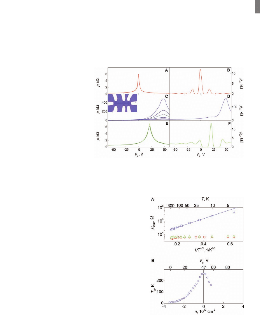
Fig. 1. Control of the electronic properties of graphene by hydrogenation. The electric field effect for
one of our devices at zero B at various temperatures T (left column) and in B = 14 T at 4 K (right). (A
and B) The sample before its exposure to atomic hydrogen; curves in (A) for three temperatures (40, 80,
and 160 K) practically coincide. (C and D) After atomic hydrogen treatment. In (C), temperature
increases from the top; T = 4, 10, 20, 40, 80, and 160 K. (E and F) The same sample after annealing.
(E) T = 40, 80, and 160 K, from top to bottom. (Inset) Optical micrograph of a typical Hall bar device.
The scale is given by its width of 1
mm.
Fig. 2. Metal-insulator transition in
hydrogenated graphene. (A) Tem-
perature dependence of graphene
’s
resistivity at NP for the sample shown
in Fig. 1. Red circles, blue squares,
and green triangles are for pristine,
hydrogenated, and annealed graphene,
respectively. The solid line is a fit by
the variable-range hopping depen-
dence exp[(T
0
/T)
1/3
]. (B) Characteristic
exponents T
0
found from this fitting
at different carrier concentrations.
www.sciencemag.org SCIENCE VOL 323 30 JANUARY 2009
611
REPORTS
on July 10, 2009
Downloaded from
the peaks in
r
xx
at
n = 0 and n = T4 became
notably greater (~40%) than that between all the
other peaks for both annealed and original de-
vices. The greater distance indicates the pres-
ence of mid-gap states (25) [such as vacancies
(26)] that were induced during the processing,
which was in agreement with the observed sub-
linear behavior of the conductivity. The extra
charge required to fill these states (25) yields their
density as of about 1 × 10
12
cm
−2
(with an aver-
age spacing of
≈10 nm).
The changes induced by hydrogenation have
been corroborated by Raman spectroscopy. The
main features in the Raman spectra of carbon-
based materials are the G and D peaks that lie at
around 1580 and 1350 cm
−1
, respectively. The G
peak corresponds to optical E
2g
phonons at the
Brillouin zone center, whereas the D peak is
caused by breathing-like modes (corresponding to
transverse optical phonons near the K point) and
requires a defect for its activation via an interval-
ley double-resonance Raman process (19, 27–29).
Both the G and D peaks arise from vibrations of
sp
2
-hybridized carbon atoms. The D peak inten-
sity provides a convenient measure for the amount
of disorder in graphene (27–29). Its overtone, the
2D peak, appears around 2680 cm
−1
and its shape
identifies monolayer graphene (19). The 2D peak
is present even in the absence of any defects be-
cause it is the sum of two phonons with opposite
momentum. In Fig. 3, there is also a peak at
~1620 cm
−1
, called D
′, which occurs via an in-
travalley double-resonance process in the pres-
ence of defects.
Figure 3A shows the evolution of Raman
spectra for graphene crystals that are hydrogenated
and annealed simultaneously with the device in
Fig. 1 (the use of different samples for Raman
studies was essential to avoid an obscuring con-
tribution to the D and D
′ peaks caused by the
edges of the Hall bars, which were smaller than
our laser spot size of about 1
mm). Hydrogenation
resulted in the appearance of sharp D and D
′
peaks, slight broadening and a decrease of the
height of the 2D peak relative to the G peak, and
the onset of a combination mode (D + D
′) around
2950 cm
−1
, which, unlike the 2D and 2D
′ bands,
requires a defect for its activation because it is a
combination of two phonons with different mo-
mentum. The D peak in hydrogenated graphene is
observed at 1342 cm
−1
and is very sharp, as com-
pared with that in disordered or nanostructured
carbon-based materials (29). We attribute the
activation of this sharp D peak in our hydrogenated
samples to breaking of the translational symmetry
of C-C sp
2
bonds after the formation of C-H sp
3
bonds. Although the majority of carbon bonds in
hydrogenated graphene are expected to acquire sp
3
hybridization, we do not expect to see any Raman
signature of C-C sp
3
bonds because their cross
section at visible light excitation is negligible as
compared with that of the resonant C-C sp
2
bonds,
and therefore even a small residual sp
2
phase
should generally dominate our spectra, as happens
in other diamondlike compounds (22, 29).
After annealing, the Raman spectrum recov-
ered to almost its original shape, and all of the
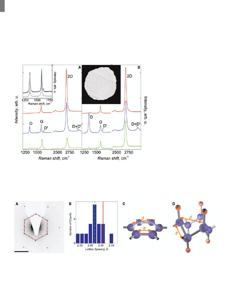
Fig. 4. Structural studies of graphane via TEM [we used a Tecnai F30 (FEI,
Eindhoven, the Netherlands)]. (A) Changes in the electron diffraction after
~4 hours exposure of graphene membranes to atomic hydrogen. Scale bar,
5 nm
−1
. The blue hexagon is a guide to the eye and marks positions of the
diffraction spots in graphane. The equivalent diffraction spots in graphene
under the same conditions are shown by the red hexagon. (B) Distribution of
the lattice spacing d found in hydrogenated membranes. The green dashed
line marks the average value, whereas the red solid line shows d always
observed for graphene (both before hydrogenation and after annealing). (C and
D) Schematic representation of the crystal structure of graphene and theo-
retically predicted graphane. Carbon atoms are shown as blue spheres, and
hydrogen atoms are shown as red spheres.
Fig. 3. Changes in Raman spectra of graphene caused by hydrogenation. The spectra are normalized to
have a similar intensity of the G peak. (A) Graphene on SiO
2.
(B) Free-standing graphene. Red, blue,
and green curves (top to bottom) correspond to pristine, hydrogenated, and annealed samples, re-
spectively. Graphene was hydrogenated for ~2 hours, and the spectra were measured with a Renishaw
spectrometer at wavelength 514 nm and low power to avoid damage to the graphene during mea-
surements. (Left inset) Comparison between the evolution of D and D
′ peaks for single- and double-
sided exposure to atomic hydrogen. Shown is a partially hydrogenated state achieved after 1 hour of
simultaneous exposure of graphene on SiO
2
(blue curve) and of a membrane (black curve). (Right inset)
TEM image of one of our membranes that partially covers the aperture 50
mm in diameter.
30 JANUARY 2009 VOL 323 SCIENCE www.sciencemag.org
612
REPORTS
on July 10, 2009
Downloaded from

defect-related peaks (D, D
′, and D+D′) were
strongly suppressed. However, two broad low-
intensity bands appeared, overlapping a sharper
G and residual D peaks. These bands are indi-
cative of some residual structural disorder (29).
The 2D peak remained relatively small with re-
spect to the G peak when compared with the
same ratio in the pristine sample, and both be-
came shifted to higher energies, indicating that
the annealed graphene is p-doped (30). The ob-
served changes in Raman spectra are in broad
agreement with our transport measurements.
For graphene on a substrate, only one side is
accessible to atomic hydrogen, and the plasma
exposure is not expected to result in graphane
(which assumes hydrogen atoms attached on
both sides). For more effective hydrogenation,
we employed free-standing graphene membranes
(Fig. 3B, inset) (20, 21). The experiments de-
scribed below refer to membranes that had some
free edges to facilitate the relaxation of strain
induced by hydrogenation [membranes with all
the sides fixed to a metal scaffold are discussed
in (22)]. Raman spectra for hydrogenated and
subsequently annealed membranes (Fig. 3B)
were rather similar to those described above for
graphene on SiO
2
, but with some notable dif-
ferences. If hydrogenated simultaneously and be-
fore reaching the saturation, the D peak for a
membrane was by a factor of two greater than
that for graphene on a substrate (Fig. 3A, inset),
which indicates the formation of twice as many
C-H bonds in the membrane. This result agrees
with the general expectation that atomic hydrogen
attaches to both sides of membranes. Moreover,
the D peak could become up to three times greater
than the G peak after prolonged exposures of
membranes to atomic hydrogen (Fig. 3B).
Further information about hydrogenated mem-
branes was obtained with TEM. For graphene,
the electron-diffraction (ED) patterns observed on
dozens of the studied membranes were always
the same, exhibiting the hexagonal symmetry with
the lattice constant d = 2.46 T 0.02 Å. Prolonged
exposure to atomic hydrogen preserved the hex-
agonal symmetry and hence crystallinity, but led
to drastic changes in the lattice constant d, which
could decrease by as much as 5% (Fig. 4A). Gen-
erally, the compression was not uniform, and
different parts of membranes exhibited locally
different in-plane periodicities (Fig. 4B; diame-
ters of the selected area for the ED and studied
membranes were 0.3
mm and 30 to 50 mm, re-
spectively). Such nonuniformity is generally not
unexpected because the crystals were fixed to
the scaffold (Fig. 3) that restricted their isotropic
shrinkage. We found that the more extended free
edges a membrane had, the more uniformly it
became hydrogenated (22). In the extreme case of
all the edges being fixed to the scaffold, even
domains with a stretched lattice could be ob-
served (22). Annealing led to complete recovery
of the original periodicity observed in TEM.
The in-plane compression of graphene
’s lat-
tice can only be the result of chemical modi-
fication as opposed to physical forces, because
any compression that is not stabilized on an
atomic scale should cause the membranes to
buckle. Furthermore, strains of the order of a few
percent would result in massive variations of the
Raman peaks, which was not the case. The most
obvious candidate for the modified crystal lattice
is graphane (7, 8). In this until-now-theoretical
material, hydrogen attaches to graphene
’s sub-
lattices A and B from the two opposite sides,
and carbon atoms in A and B move out of the
plane (
“buckle”), as shown in Fig. 4D. The in-
plane periodicity probed by TEM would then
substantially shrink if the length a of the C-C
bond were to remain the same as in graphene
(1.42 Å). However, the change in hybridization
from sp
2
to sp
3
generally results in longer C-C
bonds, which is the effect opposing to the lattice
shrinkage by atomic-scale buckling. Recent cal-
culations (8) predicted a in graphane to be ≈1.53 Å
(near that of diamond) and the in-plane peri-
odicity d to be ≈1% smaller than in graphene.
Although the maximum in the observed distri-
bution of d occurs at ≈2.42 Å (that is, near the
theoretical value for graphane) (Fig. 4B), the
observation of more compressed areas (such as
in Fig. 4A) suggests that the equilibrium d (with-
out strain imposed by the scaffold) should be
smaller. The latter implies either shorter or stron-
ger buckled C-C bonds, or both, are present. Al-
ternatively, the experimentally produced graphane
may have a more complex hydrogen bonding
than the one suggested by theory.
Finally, let us return to the graphene hydro-
genated on a substrate (Figs. 1 and 3). Single-
sided hydrogenation of ideal graphene would
create a material that is thermodynamically un-
stable (7, 8), and therefore our experiments seem
to be in conflict with the theory [for the case of
graphene on a substrate, we can exclude the pos-
sibility of double-sided hydrogenation because
the diffusion of hydrogen along the graphene-
SiO
2
interface is negligible (31)]. However, re-
alistic graphene samples are not microscopically
flat but always rippled (20, 21), which should
facilitate their single-sided hydrogenation. Indeed,
attached hydrogen is expected to change the hy-
bridization of carbon from sp
2
to (practically)
sp
3
with angles of ~110° acquired between all of
the bonds (7). These constraints necessitate the
movement of carbon atoms out of the plane in
the direction of the attached hydrogen, at the
cost of an increase in elastic energy. However,
for a convex surface, the lattice is already de-
formed in the direction that favors sp
3
bonding,
which lowers the total energy. As shown in (22),
single-sided hydrogenation becomes energetical-
ly favorable for a typical size of ripples observed
experimentally (20). Because of the random na-
ture of ripples, single-sided graphane is expected
to be a disordered material, similar to graphene
oxide, rather than a new graphene-based crystal.
The formation of a disordered material also ex-
plains the observation of variable-range hopping
in our transport experiments. The importance of
ripples for hydrogenation of graphene on a sub-
strate is further evidenced in experiments involv-
ing bilayer samples, which show a substantially
lower level of hydrogenation than monolayers
under the same conditions (22). We attribute this
observation to the fact that bilayer graphene is
less rippled (20).
The distinct crystal structure of hydrogenated
graphene and pronounced changes in its electronic
and phonon properties reveal two new graphene
derivatives, one crystalline and the other disordered.
The results show that conversion of graphene into
other giant molecules with a regular structure is
possible.
References and Notes
1. A. K. Geim, K. S. Novoselov, Nat. Mater. 6, 183 (2007).
2. S. Stankovich et al., J. Mater. Chem. 16, 155 (2006).
3. S. Stankovich et al., Nature 442, 282 (2006).
4. X. Wang, L. Zhi, K. Mullen, Nano Lett. 8, 323 (2008).
5. S. Gilje, S. Han, M. Wang, K. L. Wang, R. B. Kaner, Nano
Lett. 7, 3394 (2007).
6. C. Gomez-Navarro et al., Nano Lett. 7, 3499 (2007).
7. J. O. Sofo, A. S. Chaudhari, G. D. Barber, Phys. Rev. B 75,
153401 (2007).
8. D. W. Boukhvalov, M. I. Katsnelson, A. I. Lichtenstein,
Phys. Rev. B 77, 035427 (2008).
9. A. C. Dillon et al., Nature 386, 377 (1997).
10. F. L. Darkrim, P. Malbrunot, G. P. Tartaglia, Int. J.
Hydrogen Energy 27, 193 (2002).
11. A. Züttel et al., Int. J. Hydrogen Energy 27, 203 (2002).
12. T. Yildirim, O. Gulseren, S. Ciraci, Phys. Rev. B 64,
075404 (2001).
13. B. N. Khare, M. Meyyappan, A. M. Cassell, C. V. Nguyen,
J. Han, Nano Lett. 2, 73 (2002).
14. P. Ruffieux et al., Phys. Rev. B 66, 245416 (2002).
15. D. Neumann et al., Appl. Phys. A 55, 489 (1992).
16. A. Nikitin et al., Phys. Rev. Lett. 95, 225507 (2005).
17. L. Hornek
æ
r et al., Phys. Rev. Lett. 96, 156104 (2006).
18. K. S. Novoselov et al., Science 306, 666 (2004).
19. A. C. Ferrari et al., Phys. Rev. Lett. 97, 187401 (2006).
20. J. C. Meyer et al., Nature 446, 60 (2007).
21. T. J. Booth et al., Nano Lett. 8, 2442 (2008).
22. Supporting online material is available on Science
Online.
23. S. V. Morozov et al., Phys. Rev. Lett. 100, 016602
(2008).
24. N. F. Mott, Philos. Mag. 19, 835 (1969).
25. T. O. Wehling et al., Nano Lett. 8, 173 (2008).
26. V. M. Pereira, F. Guinea, J. M. B. Lopes dos Santos,
N. M. R. Peres, A. H. Castro Neto, Phys. Rev. Lett. 96,
036801 (2006).
27. A. C. Ferrari, Solid State Commun. 143, 47 (2007).
28. F. Tuinstra, J. L. Koenig, J. Chem. Phys. 53, 1126 (1970).
29. A. C. Ferrari, J. Robertson, Phys. Rev. B 61, 14095 (2000).
30. A. Das et al., Nat. Nanotechnol. 3, 210 (2008).
31. J. S. Bunch et al., Nano Lett. 8, 2458 (2008).
32. This work was supported by Engineering and Physical
Sciences Research Council (UK), the Royal Society, the
European Research Council (programs
“Ideas” and “New
and Emerging Science and Technology,
” project
“Structural Information of Biological Molecules at Atomic
Resolution
”), Office of Naval Research, and Air Force
Research Office of Scientific Research. D.C.E. acknowledges
financial support from the National Council for Scientific
and Technological Development (Brazil). The authors are
grateful to Nacional de Grafite for providing high-quality
crystals of natural graphite.
Supporting Online Material
www.sciencemag.org/cgi/content/full/323/5914/610/DC1
SOM Text
Figs. S1 to S7
References
13 October 2008; accepted 10 December 2008
10.1126/science.1167130
www.sciencemag.org SCIENCE VOL 323 30 JANUARY 2009
613
REPORTS
on July 10, 2009
Downloaded from
Wyszukiwarka
Podobne podstrony:
312[01] 05 092 CZERWIEC 2009 id Nieznany (2)
312[01] 04 091 STYCZEN 2009 id Nieznany (2)
50 Science 306 666 669 2004 id Nieznany (2)
312[01] 02 092 CZERWIEC 2009 id Nieznany
matura 2009 dwu a1 DWU m2009 id Nieznany
matura 2009 dwu a2 DWU m2009 id Nieznany
CAD ZADANIA 1 2009 id 107691 Nieznany
LCCI Level 1 rok 2009 id 263960 Nieznany
26(2009) art23 Modelowanie id 3 Nieznany
prawo pracy skrypt 2009 2010 id Nieznany
objpit 37 2009 id 327255 Nieznany
Matura 2009 id 288649 Nieznany
2009 10 13 Wstep do SI [w 01]id Nieznany
więcej podobnych podstron